Note: Descriptions are shown in the official language in which they were submitted.
CA 03051602 2019-07-25
1
Magnetic force sensor and production thereof
The invention relates to a magnetic force sensor having at least one
conducting track of soft
magnetic material, wherein the at least one conducting track has at least one
interruption
having a distance, and to a manufacturing method for producing the magnetic
force sensor.
The measurement of physical quantities on components of for example, vehicles
and
aircraft, machines or buildings is an essential element for their maintenance
and operations
monitoring. An important factor in this connection is the force acting on a
component, the
measurement of which provides important information about the load or the
overall
condition of the component.
The method which is currently most commonly used consists in the measurement
of
deformations and the forces arising thereby by means of strain gauges attached
to
appropriate spots of the component. A major disadvantage of this system is
that those strain
gauges are glued to the component to be measured, with this bonding affecting
the
transmission of the measured information, possibly falsifying it. Furthermore,
the strain
gauge must be electrically contacted so that the measured information can be
read out,
wherein it is necessary for metallic components to completely isolate the
electrical
measuring circuit from the component.
Therefore, methods have become known wherein the measurement of deformations
of a
component is conducted by magnetic means.
For example, DE 10 2014 200 461 AI describes an arrangement for measuring a
force or a
torque on a machine element with a permanent magnetization along a closed
magnetization
path. For this, a magnetic field sensor is provided which monitors a change in
the magnetic
field. This arrangement is not suitable for all components, since it requires
a permanent
magnetization of the component at least in a certain area. It is also
susceptible to faults with
regard to magnetic and/or electrical or, respectively, electromagnetic
influences from the
outside.
In DE 36 24 846 Al, a device for contactless measurement of a mechanical
stress, in
particular for measuring the torsion or bending force of a measured object, is
described. For
this purpose, two regions comprising a layer of magnetoelastic material, which
has a stripe
pattern formed at an angle of 45 , are arranged on a shaft. A change in this
layer pattern
when the shaft is under mechanical stress is monitored using a complex
evaluation circuit.
CA 03051602 2019-07-25
2
Another magnetoelastic torque sensor can also be found in DE 103 31 128 Al.
US 5,036,236 A discloses a proximity sensor based on magnetic fields, wherein
the sensor
comprises a magnetic conductor having an interruption serving as a reference
for the
distance between two components of magnetic material moving toward each other.
The above-mentioned arrangements are only partially, or not at all, suitable
for monitoring
deformation processes on a component or have a complex structure which, in
practice, is not
very suitable.
It is therefore the object of the invention to provide a magnetic force sensor
which is suitable
for monitoring deformation processes on a component made also of non-magnetic
material,
wherein the sensor can be arranged at arbitrary spots of the component to be
monitored.
According to the invention, this object is achieved in that the force sensor
according to the
invention is arranged on a substrate, preferably directly on the component to
be monitored,
wherein a change in the distance of the interruption of the at least one
magnetic conducting
track is monitored. In a first embodiment of the invention, the force sensor
according to the
invention has a particularly simple structure and can be arranged on any
desired ground.
In this case, the magnetic flux in the at least one magnetic conducting track
is monitored,
wherein a change in the distance of the at least one magnetic conducting track
causes a
change in the magnetic flux in the at least one magnetic conducting track. In
case of a
possible deformation of the component to be monitored due to forces acting on
it, the
distance of the at least one interruption of the at least one magnetic
conducting track
changes. This, however, changes the magnetic field induced in the interruption
of the at least
one magnetic conducting track, whereby the magnetic flux in the at least one
magnetic
conducting track changes in turn. This change in the magnetic flux is thus an
indicator of a
deformation of the component to be monitored.
Different processes can be used as measuring methods for a change in the
magnetic flux,
namely inductive ones, those according to the fluxgate principle, those via
the anisotropic
magnetic resistance or those using magnetoimpedance.
CA 03051602 2019-07-25
3
If the measurement of the flux change is conducted inductively, rapid flux
changes can be
measured in this case, this method being unsusceptible to slow changes which
occur
gradually. Furthermore, absolute magnetic flux values cannot be determined by
this method.
With the anisotropic magnetoresistive effect, the electric resistance of a
ferromagnetic
material changes with its magnetization, wherein this change in resistance can
be measured.
The magnetoimpedance effect is based, on the one hand, on the change in the
differential
permeability of a soft magnetic substance as a function of the magnetization
thereof, and on
the so-called skin effect due to which the current in a conductor is forced
through its own
magnetic field toward the surface at high frequencies. Combined, those effects
cause the AC
resistance of a soft magnetic conductor to be highly dependent on an external
magnetic field;
this effect can be observed particularly well at frequencies in the MI-lz
range.
Fluxgate sensors are able to precisely measure small magnetic fluxes, this
type of
measurement being more complex, as the measuring sections must be surrounded
by coils
for this purpose.
Each of those measuring methods is suitable for detecting the change in the
distance of the at
least one interruption in the at least one conducting track of the magnetic
measuring circuit.
Preferably, the measured value for the magnetic flux is permanently compared
to a
predefinable threshold value in an evaluation unit, and upon reaching this
threshold value, a
signal is emitted. This signal serves as a warning signal when the component
to be monitored
deforms, whereby the change in the distance of the at least one interruption
in the magnetic
conducting track is induced.
According to the invention, it is provided in a first embodiment of the
invention that the
substrate consists of an insulating material, e.g., plastic, ceramic, glass,
sapphire or mica. In
this case, the force sensor according to the invention is applied to this
substrate, for example,
by means of electrodeposition, and the substrate is, in turn, arranged on the
component to be
measured.
As an alternative, it is provided in a particularly preferred variant that the
force sensor is
applied directly to the component, in particular by means of
electrodeposition. In this case, it
may be provided that the force sensor is provided with a magnetic barrier
layer of non-
CA 03051602 2019-07-25
4
magnetic material in order to isolate the force sensor according to the
invention from a
magnetizable component, thus protecting it from interfering influences.
In order to produce a magnetic flux in the force sensor, at least one
excitation magnet is
provided in a particularly preferred embodiment of the invention. Said magnet
may be a
permanent magnet, which preferably is also produced by means of
electrodeposition. For this
purpose, a hard magnetic alloy is deposited, or permanently magnetic particles
may also be
incorporated in a non-magnetic matrix. As an alternative, the excitation
magnet may also be
an electromagnet.
Preferably, it is provided that the magnetic flux in the at least one
conducting track is
induced by at least one excitation magnet, which is preferably in direct
contact with the at
least one magnetic conducting track. Alternatively, however, the at least one
excitation
magnet can be formed also outside of the force sensor, for example as part of
the component
to be monitored or as an additional element in the region of the component to
be monitored.
The force sensor according to the invention is preferably provided with at
least one
measuring device for monitoring the magnetic flux within the at least one
conducting track.
In this manner, an integral measuring sensor is obtained without the need for
an additional
external measuring unit.
In this connection, it is particularly preferably provided that the at least
one measuring
device is designed as a measuring chip with at least one, preferably two,
internal magnetic
measuring sections, the measuring chip preferably being arranged on an
electrically
insulating carrier, e.g., plastic, ceramic, glass, sapphire or mica. Said
measuring chip
analyses the changes in the magnetic flux and transmits the obtained data to
an (external)
evaluation unit.
In a particularly preferred embodiment of the invention, it is provided that
the at least one
magnetic conducting track with the at least one interruption and the at least
one measuring
device form a magnetic measuring circuit. In this case, the at least one
excitation magnet is
advantageously also part of said magnetic measuring circuit. Alternatively,
the at least one
excitation magnet can be arranged outside of the force sensor.
In interference-prone environments, it may be necessary to compensate for
external effects
such as stray fields or temperature fluctuations that affect the magnetic flux
independently of
a force. For this purpose, a second magnetic circuit, namely a magnetic
compensation circuit
CA 03051602 2019-07-25
preferably with at least one further excitation magnet, is provided. The
adjustment of the
magnetic resistance of the compensation circuit can optionally be achieved by
influencing
the permeability of the magnetic conductor during the production, namely the
deposition, for
example by varying the pulse pattern used for the deposition, by geometric
variations such as
layer thickness and/or conductor width, by introducing an additional
interruption of the
magnetic conductor of the compensation circuit at a suitable location or by a
combination of
those measures.
The at least one measuring device, in particular the measuring chip, connects
the two
magnetic circuits, namely the at least one measuring circuit and the at least
one
compensation circuit, preferably via a Wheatstone bridge. This design allows
even the
smallest changes in the magnetic flux to be measured accurately.
The force sensor according to the invention is used in particular for the
determination of
deformations of components.
The production of the force sensor according to the invention is effected by
means of a
manufacturing method wherein at least one magnetic conducting track having at
least one
interruption is applied to a substrate, preferably to a component to be
monitored, involving a
distance, wherein the application is effected particularly preferably by means
of
electrodeposition.
In doing so, a soft magnetic alloy, e.g., a nickel-iron alloy of an optimized
composition, is
applied to a preferably non-magnetic, optionally masked component by galvanic
means. In
this case, the interruption with a defined distance, which is required for the
measurement,
either is created already in the masking or is incorporated after the coating,
for example
using a laser.
If the ground on which the force sensor is applied is magnetic, e.g., made of
steel or cast
iron, a non-magnetic layer must be applied to the base material prior to the
application of the
conducting tracks. This non-magnetic layer is, for example, a layer of copper,
tin, zinc,
which has also been produced galvanically, or an alloy of two or more of those
elements or
else also of a non-magnetic alloy of iron metals with phosphorus. Due to this
fully metallic
structure, an optimum connection of the sensor to the component is obtained
without, for
example, an additional adhesive layer for applying the sensor to the component
to be
measured being able to influence the measurement results.
CA 03051602 2019-07-25
6
The galvanic production of the excitation magnets, which are particularly
suitable for the
force sensor according to the invention, can be accomplished in two different
ways.
In one variant, a permanently magnetic alloy selected from a group comprising
alloys such
as cobalt-nickel-phosphorus, cobalt-nickel-manganese-phosphorus, cobalt-nickel-
rhenium-
phosphorus, iron-platinum, cobalt-platinum and bismuth-manganese, is
electrodeposited on
the substrate or, respectively, component.
As an alternative, permanently magnetic micro- or nanoparticles are
incorporated into a non-
magnetic, metallic matrix during the electrodeposition on the substrate, in
particular the
component. In this case, all hard magnetic materials are suitable as
particles, just as hard
magnetic alloys in a suitable form, e.g., as nanowires, as powders such as,
e.g., ferrites,
chromium dioxide, iron oxide, neodymium-iron-boron powder or cobalt-samarium
powder.
Those particles can be used either in pure form or following a suitable
chemical surface
modification, for example with siloxanes. On the one hand, the chemical
modification of the
surface of the particles serves for the control of the incorporation rate of
the particles into the
galvanic layer, on the other hand, the chemical stability against the
electrolyte used for the
deposition can thereby be increased.
Preferably, the deposition of the permanently magnetic layer occurs in a
magnetic field
applied from the outside, which aligns the particles in their direction of
magnetization and
thus increases the resulting field strength of the electrodeposited permanent
magnet.
For special requirements, it is possible to perform the deposition of the
permanently
magnetic layer in several phases and to change the direction of the external
magnetic field
between the phases. In this way, permanently magnetic layers with a locally
varying
magnetization can be produced.
The invention is explained in further detail below on the basis of non-
limiting exemplary
embodiments with associated figures. Therein:
Fig. I shows a schematic view of a first embodiment of the force sensor
according to the
invention;
Fig. 2 shows a detailed view of the magnetic conducting track of the force
sensor of Fig. I;
Fig. 3 shows a detailed view of the measuring chip of Fig. I;
Fig. 4 shows a schematic illustration of the layer structure of the force
sensor of Fig. I; and
CA 03051602 2019-07-25
7
Fig. 5 shows a schematic view of a second embodiment of the force sensor
according to the
invention.
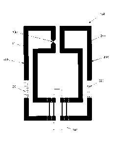
In Fig. I, a first particularly preferred embodiment of the force sensor 100
according to the
invention is depicted. This force sensor 100 comprises a magnetic measuring
circuit 110
with a magnetic conducting track 111 in which a first excitation magnet 120 is
arranged.
This magnetic conducting track 111 has an interruption 130, wherein the two
ends of the
magnetic conducting track 112A, 112B are arranged at a distance A from each
another, and
their two ends 112A, 1 I 2B taper in their cross-sections (see Fig. 2). Due to
this tip or arrow-
shaped formation of the two ends 112A, 112B of the magnetic conducting track
111,
particularly strong magnetic field lines are established in this area, whereby
a more precise
measurement of a possible change in the distance A between the two ends 112A,
112B and,
hence, of a possible change in the magnetic field between the two ends 112A,
112B is
rendered possible.
In order to minimize influences, in particular magnetic and/or electromagnetic
influences
from the environment, the force sensor 100 according to the invention
additionally
comprises, in this embodiment of the invention, a compensation measuring
circuit 210 with a
magnetic conducting track 211, which compensation measuring circuit is
likewise provided
with a second excitation magnet 220. The magnetic fluxes of the two
magnetically active
measuring circuits 110, 210 are measured relative to each other another via a
measuring chip
300.
Said measuring chip 300 is depicted in detail in Fig. 3. It is applied to an
electrically
insulating base 310 in order to electrically insulate it from the metal
ground, namely the
component to be monitored. This electrically insulating base 310 is made, for
example, of
ceramic, plastic, mica or similar insulating materials.
The magnetic conductor 111 of the magnetic measuring circuit 110 couples with
its two
second ends to the two magnetic inputs 31 I A, 311 B of the measuring chip
300. For this
purpose, the two inputs 31 I A, 311B have a magnetic coupling by means of
ferrite 312 along
with a concurrent electrical insulation. Between the two inputs 311 A, 311B,
two magnetic
measuring sections 3 I 3A, 313B are provided, which serve for monitoring the
interruption
130 having the distance A of the magnetic conductor 111.
CA 03051602 2019-07-25
8
Also for the compensation circuit 210, magnetic inputs 311C, 311D are provided
on the
measuring chip 300, which, in turn, are interconnected via two measuring
sections 313C,
313D.
Finally, connections 320 for supplying the measuring chip 300 with electric
current and
signal outputs 330 for evaluating the obtained measuring signals are provided.
The mode of operation of the force sensor 100 according to the invention can
be described as
follows:
During the monitoring of a component on which the force sensor 100 is applied,
both the
magnetic measuring circuit 110 and the compensation circuit 210 have a
constant magnetic
field. However, if a deformation of the component occurs in the region of the
interruption
130 of the magnetic measuring circuit 110, the distance A of the interruption
130 and thus
the induced magnetic field change, with the resulting change in the magnetic
flux in the
measuring circuits 110, 210 being detected via the measuring sections 313A,
313B, 313C,
313D. This change in the magnetic flux can be analysed in an appropriate
evaluation
electronics (not shown), and, for example, a warning regarding the stability
of the
component can optionally be issued.
A further embodiment of the force sensor 100 according to the invention is
depicted in Fig.
4. In this case, the force sensor 100 has a two-part design, with a first
part, the monitoring
part 100A, being arranged on a component 1 to be monitored. A second part, the
measuring
part 100B of the force sensor 100, is arranged on a second component 2 spaced
apart from
the first component 1 via a gap 3.
The external magnetic measuring circuit 110 rests with a first part 110A, the
magnetic
conducting track 111 of which comprises the interruption 130, on the component
1 to be
monitored, whereas its second part 110B is arranged with an excitation magnet
120 on the
component 2. Similarly, the internal magnetic compensation circuit 210 has a
two-part
design, namely with a first part 2I0A being arranged on the first component 1
and with its
second part 210B being arranged with its conducting track 211 on the second
component 2.
In each case, the conducting tracks 111, 2 I 1 end in the measuring chip 300.
This two-part structure of the force sensor 100 according to the invention
with two
interruptions, namely the interruption 130 of the magnetic conducting track
111 and the gap
3, across two components 1, 2 allows monitoring of a possible deformation of
the first
CA 03051602 2019-07-25
9
component 1. In this case, as already described above, the distance A in the
interruption 130
and thus the magnetic flux within the force sensor 100 change with a
deformation of the first
component 1. At the same time, however, the position of the two components 1,
2 relative to
each other is also monitored. Since the two excitation magnets 120, 220 are
arranged on the
second component 2 in close proximity to the conducting tracks 111, 112 on the
first
component 1, the magnetic flux changes again when the gap 3 between the two
components
1, 2 is enlarged or reduced, or else the position of the first component 1
shifts in relation to
the second component 2, without their mutual distance being changed.
If the component 1 to be monitored is produced from a magnetic material, it is
necessary to
apply the magnetic measuring circuit 110 and optionally the compensation
circuit 210 on
this component 1 in an insulated manner. In a further embodiment of the
invention - as
illustrated in Fig. 5 - it is provided for this purpose that a non-magnetic
insulating layer 10
made of, for example, copper, tin, zinc or an alloy of those elements, but
also of a non-
magnetic alloy of ferrous metals with phosphorus, is applied by means of
galvanic methods.
Subsequently, the magnetic measuring circuit 110 with the associated
excitation magnet 120
is also electrodeposited on this non-magnetic layer 10.