Note: Descriptions are shown in the official language in which they were submitted.
CA 03052056 2019-07-29
WO 2018/144610
PCT/US2018/016252
OPTICAL SYSTEM FOR MANAGING LIGHT FROM A LIGHT EMITTING
DIODE
RELATED APPLICATIONS
The present application claims priority under 35 U.S.C. 119(e) to U.S.
Provisional Patent Application No. 62/452,811, filed January 31, 2017, and
titled
"Optical System For Managing Light From a Light Emitting Diode," the entire
contents
of which are incorporated herein by reference.
TECHNICAL FIELD
Embodiments of the technology relate generally to illumination systems and
more
particularly to an optical system that manages light from at least one light
emitting diode
(LED).
BACKGROUND
For illumination applications, light emitting diodes offer substantial
potential
benefits associated with their energy efficiency, light quality, and compact
size.
However, to realize the full potential benefits offered by light emitting
diodes, new
technologies are needed.
For instance, there are needs in the art for managing light emitted by single
light
emitting diodes, large chip-on-board (COB) light emitting diodes, and arrays
of light
emitting diodes. Such needs include improvements for processing the emitted
light from
one or more light emitting diodes in a manner that provides controlled
illumination, for
example in a high-output lighting system that may be suitable for illuminating
a football
field or another sporting venue. Such needs also include improved optics that
are
compact in size and that can process light from light emitting diodes that are
larger in
size.
A capability addressing one or more such needs, or some other related
deficiency
in the art, would support improved illumination systems and more widespread
utilization
of light emitting diodes in illumination applications.
1
CA 03052056 2019-07-29
WO 2018/144610
PCT/US2018/016252
SUMMARY
In one embodiment, the present disclosure is directed to an optic comprising a
rear surface with a cavity configured to receive light from a light source.
The optic
further comprises a front surface configured to emit light processed by the
optic, the front
surface comprising a centrally disposed convex region. The front surface and
the rear
surface of the optic meet to form a rim that extends peripherally with respect
to the
cavity. The front surface further comprising a concave region disposed between
the rim
and the centrally disposed convex region, the concave region extending
peripherally
about the centrally disposed convex region.
1 0 In
another embodiment, the present disclosure is directed to a system comprising
an optic and a reflector. The optic comprises a rear surface with a cavity
configured to
receive light from a light source and a front surface opposite the rear
surface, the front
surface configured to emit light processed by the optic and the front surface
comprising a
centrally disposed convex region. The front surface and the rear surface of
the optic meet
at a rim that extends peripherally with respect to the cavity. The reflector
is disposed
adjacent the optic and comprises a light-receiving end adjoining the rim, a
light-emitting
end, and a tapered region that extends between the light-receiving end and the
light-
emitting end.
In yet another embodiment, the present disclosure is directed to a lighting
system
comprising a substrate, at least one light emitting diode mounted on the
substrate, an
optic mounted on the substrate, and a reflector. The optic comprises a cavity
disposed to
receive light from the at least one light emitting diode, a totally internally
reflective
surface that extends circumferentially about the cavity, a refractive surface
that is
disposed to emit an emitted light, and a rim formed between the totally
internally
reflective surface and the refractive surface. The reflector comprises a light-
receiving
end that adjoins the rim and a light-emitting end opposite the light-receiving
end. In one
example, the reflector can be mounted to the substrate so that physical
contact between
the optic and the hollow reflector occurs only at the rim. In another example,
the
reflector can be mounted to the substrate so that a gap exists between the
light-receiving
end of the reflector and the rim. In yet another example, the cavity of the
optic can
comprise at least one side wall, wherein the at least one side wall comprises
a plurality of
2
CA 03052056 2019-07-29
WO 2018/144610
PCT/US2018/016252
angled facets configured to reduce refraction of a portion of the light
received from the
light source. In yet another example, the cavity can comprise a widest cavity
diameter
and the light source comprises a widest light source diameter, wherein the
widest light
source diameter is more than one half of the widest cavity diameter.
These and other aspects, objects, features, and embodiments will be apparent
from
the following description and the appended claims.
BRIEF DESCRIPTION OF THE FIGURES
The drawings illustrate only example embodiments of methods, systems, and
1 0
devices for optical systems comprising a refractor and a reflector and are
therefore not to
be considered limiting in scope, as they may admit to other equally effective
embodiments. The elements and features shown in the drawings are not
necessarily to
scale, emphasis instead being placed upon clearly illustrating the principles
of the
example embodiments.
Additionally, certain dimensions or positions may be
exaggerated to help visually convey such principles. In the drawings,
reference numerals
designate like or corresponding, but not necessarily identical, elements.
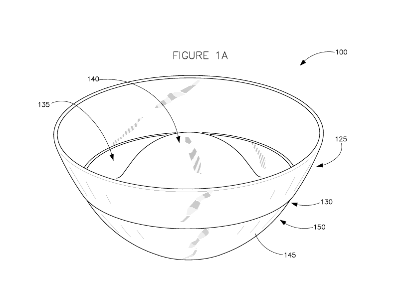
Figure 1A illustrates a side perspective view of an optical system in
accordance
with an example embodiment of the present disclosure.
Figure 1B illustrates a side view of the optical system of Figure 1A in
accordance
with an example embodiment of the present disclosure.
Figure 1C illustrates a rear view of the optical system of Figure 1A in
accordance
with an example embodiment of the present disclosure.
Figure 1D illustrates a front view of the optical system of Figure 1A in
accordance with an example embodiment of the present disclosure.
Figures 2A, 2B, and 2C illustrate side cross sectional views of the optic
portion of
the optical system of Figure 1A overlaid with representative ray traces from a
light source
in accordance with an example embodiment of the present disclosure.
3
CA 03052056 2019-07-29
WO 2018/144610
PCT/US2018/016252
Figures 3A and 3B illustrate side cross sectional views of the optical system
of
Figure lA overlaid with representative ray traces from a light source in
accordance with
an example embodiment of the present disclosure.
Figure 4 illustrates a side cross sectional view of the optical system of
Figure lA
overlaid with representative ray traces from a light source in accordance with
an example
embodiment of the present disclosure.
Figure 5 illustrates a side cross sectional view of an optic in accordance
with
another example embodiment of the present disclosure.
Figure 6 illustrates a side cross sectional view of an optical system
comprising the
example optic of Figure 5 and overlaid with representative ray traces from a
light source
in accordance with an example embodiment of the present disclosure.
Figure 7 illustrates an enlarged side cross sectional view of a portion of the
example optic of Figure 5 overlaid with representative ray traces from a light
source in
accordance with an example embodiment of the present disclosure.
Figure 8 illustrates a side cross sectional view of an optical system
comprising the
example optic of Figure 5 in accordance with an example embodiment of the
present
disclosure.
DETAILED DESCRIPTION OF EXAMPLE EMBODIMENTS
In some example embodiments as described herein, a lighting system can
comprise an optical system that receives light emitted from a light source,
for example a
light emitting diode source, and that processes (e.g., refracts, reflects, or
otherwise
modifies) the received light to provide illumination. In some example
embodiments as
described herein, the lighting system can comprise an optic or an optic and an
associated
reflector. In some example embodiments, the lighting system can be sized to
deliver a
high level of illumination in the form of a narrow beam floodlight, such as
may be
utilized in an outdoor sporting venue.
Some representative embodiments will be described more fully hereinafter with
example reference to the accompanying drawings that illustrate embodiments of
the
4
CA 03052056 2019-07-29
WO 2018/144610
PCT/US2018/016252
technology. The technology may, however, be embodied in many different forms
and
should not be construed as limited to the embodiments set forth herein;
rather, these
embodiments are provided so that this disclosure will be thorough and
complete, and will
fully convey the scope of the technology to those appropriately skilled in the
art.
The drawings illustrate only example embodiments and are therefore not to be
considered limiting of the embodiments described, as other equally effective
embodiments are within the scope and spirit of this disclosure. The elements
and features
shown in the drawings are not necessarily drawn to scale, emphasis instead
being placed
upon clearly illustrating principles of the embodiments. Additionally, certain
dimensions
or positions may be exaggerated to help visually convey certain principles. In
the
drawings, similar reference numerals among different figures designate like or
corresponding, but not necessarily identical, elements.
Figures 1A, 1B, 1C, and 1D (collectively Figure 1) illustrate an example
optical
system 100 comprising an optic 150 and an associated reflector 125. In Figure
1, the
optic 150 is illustrated as opaque to promote viewing but may be optically
clear in
physical implementation. The optic 150 can have a composition of clear
silicone, clear
acrylic, or other appropriate optical-grade polymer, for example. Figure 1A
illustrates a
side perspective view of the optical system 100. Figure 1B illustrates a side
view of the
optical system 100. Figure 1C illustrates a rear view of the optical system
100. Figure
.. 1D illustrates a front view of the optical system 100.
Figures 2A, 2B, and 2C (collectively Figure 2) illustrate a side cross
sectional
view of an example embodiment of the optic 150 overlaid with representative
rays from a
light source 155. The light source 155 can comprise one or more light emitting
diodes
and is represented as a point source in the figures. Each of the Figures 2A,
2B, and 2C
illustrates representative rays from a distinct solid angle of point-source-
emitted light to
facilitate reader viewing of the rays. Although illustrated as a point source
for simplicity
in the figures, the light source can be any one of a variety of light sources,
including but
not limited to a discrete LED, multiple LEDs, a chip on board LED, or an
organic LED.
One advantage of the example optical systems described herein is that they can
accommodate a relatively larger light source without requiring a corresponding
increase
5
CA 03052056 2019-07-29
WO 2018/144610
PCT/US2018/016252
in the size of the optical system. In other words, the size of the optic and
the reflector can
be maintained relatively small while being able to process light from a light
source
having a larger size.
Figures 3A and 3B illustrate a side cross sectional view of an example
embodiment of the optical system 100 overlaid with representative rays from
the light
source 155.
As can be best seen in Figures 1B and 2A, the optical system 100 is configured
for mounting to a substrate 161, such as a circuit board or other appropriate
element that
may provide structural support. The substrate 161 extends along a reference
plane 160.
The light source 155 may be mounted directly to the substrate 161 in some
example
embodiments. The optic 150 may also be mounted directly to the substrate 161
in some
example embodiments. In some other example embodiments, the optic 150 is
attached to
the light source 155, and the resulting unit is attached directly to the
substrate 161.
The reflector 125, which will be discussed in further detail below, may be
attached directly to the optic 150 or may be attached directly to the
substrate 161. In the
example of attaching directly to the substrate 161, the optic 150 and the
reflector 125 may
either be in contact with one another or separated slightly from one another,
for example
with a separation of less than about 0.5 mm or 1.0 mm. In some embodiments,
the optic
150 and the reflector 125 are separately attached to the substrate 161 in a
manner that
2 0 avoids physical contact with any optical surfaces of the optic 150 that
would impede the
intended optical function of the optic 150.
In the illustrated embodiment, and as can be seen in Figures 2B and 3A, the
optic
150 and the reflector 125 can be rotationally symmetrical about an axis 179.
The axis
170 can comprise an optical axis of the optic 150, the reflector 125, and the
light
source 155.
As can be seen in the cross sectional view of Figure 3A (and other figures),
in the
illustrated embodiment, the optic 150 comprises a cavity 105 that is oriented
to receive
light from the light source 155. The cavity 105 has an opening that receives
light from
the light source 155 and a sidewall 115 (for example, if the cavity is
cylindrical), or
multiple sidewalls, that extend into the body of the optic 150. The bottom of
the cavity
6
CA 03052056 2019-07-29
WO 2018/144610
PCT/US2018/016252
105 is contoured to from a convex surface 110 that condenses incident light as
can be
best seen in Figure 3B.
In the illustrated embodiment, the optic 150 further comprises a totally
internally
reflective surface 145. As can be seen in the cross section of Figure 3B
(among other
figures), the totally internally reflective surface 145 extends
circumferentially or
peripherally around the cavity 105.
As shown in Figure 2A, the illustrated example optic 150 comprises a rear
surface
177 that circumscribes the cavity 105 and may be positioned against or along
the
substrate 161, so that the rear surface 177 extends along or is in the
reference plane 160.
As illustrated, the totally internally reflective surface 145 of the optic 150
is curved in
cross section and extends laterally from the rear surface 177 to a rim 120 on
the optic
150.
The optic 150 further comprises a light-emitting side (front side) that is on
the
side opposite the rear surface 177 and the light-emitting side is
circumscribed by the rim
120. As illustrated, the light-emitting side of the optic 150 comprises a
centrally located
convex region 140 and a concave region 135. The concave region 135 is disposed
adjacent the rim 120 and extends peripherally around the convex region 140. In
the
illustrated example, the concave region 135 can be characterized as a groove.
As further
shown in the example of Figures 1A ¨ 3B, the convex region 140 and the concave
region
135 form a continuous smooth surface (or curve as viewed in cross section)
without
abrupt changes in the surface as it extends from the rim 120 on one side of
the optic 150
along the light-emitting side to the rim 120 on the opposite side of the optic
150.
As shown in the cross sectional view of Figure 2A, in the illustrated example,
the
concave region 135 has a concave region bottom that is disposed a first
distance 167 from
the reference plane 160. The center or apex of the centrally located convex
region 140 is
disposed a second distance 165 from the reference plane 160. The rim 120 is
disposed a
third distance 166 from the reference plane 160. In the illustrated example,
the first
distance 167 between the bottom of the concave region 135 and the reference
plane 160
is less than both of the second distance 165 and the third distance 166. The
third distance
166 is between the first distance 167 and the second distance 165.
7
CA 03052056 2019-07-29
WO 2018/144610
PCT/US2018/016252
As another way of characterizing a representative geometry of the illustrated
example optic 150, the concave region 135 may have a fluid-holding form. In
other
words, while the concave region 135 provides an optical function, the shape
and
orientation of the concave region 135 may be formed in a manner that could
function as a
vessel for fluid. More specifically, as illustrated, the concave region 135
and the optic
150 are configured such that the reference plane 160 can be situated
horizontal with
respect to gravity, and the optic 150 can be oriented to rest on the reference
plane (as
depicted in Figure 2A without limitation). In this hypothetical configuration,
the concave
region 135 has a form and orientation with respect to gravity such that a
liquid placed in
the concave region 135 could remain in the concave region 135.
As illustrated in Figures 1 and 3, the example reflector 125 of the optical
system
comprises a tapered reflective surface that is oriented to receive, process,
and emit light
that is emitted from the optic 150. In one embodiment, the reflector is
designed to reflect
light diffusely and can be made of white plastic, a metallized plastic, or a
spun metal. In
cross section or side view, the reflector 125 is curved in the illustrated
example. As
illustrated, the light-receiving end of the reflector 125 and the rim 120
adjoin one another
to form an interface 130. At the opposite end, light exits the reflector 125
at the light-
emitting end of the reflector. In the example illustrated embodiment, the
reflector 125
butts up to the rim 120 at the interface 130. In the illustrated embodiment,
the reflector
125 and the rim 120 can be joined using a variety of mechanisms such as co-
molding the
two components or forming a notch for one component to fit within the other.
Other
example mechanisms for joining the two components are described in connection
with
the embodiments shown in Figures 5 and 8. In yet other embodiments, the
reflector 125
may be attached to the substrate 161 and may or may not contact the optic 150.
In other
words, in some embodiments, there may be a small gap between the rim 120 of
the optic
150 and the reflector 125.
The reflector 125 and the optic 150 can be formed so that the totally
internally
reflective surface 145 of the optic 150 and the reflective surface of the
reflector 125 curve
inward at the interface 130. For example, as illustrated in Figure 1B, in some
embodiments, a line 170 may be drawn tangent to an outer surface of the
reflector 125
and further tangent to the totally internally reflective surface 145 of the
optic 150. At the
8
CA 03052056 2019-07-29
WO 2018/144610
PCT/US2018/016252
interface 130, the totally internally reflective surface 145 and the
reflective surface can be
displaced from that tangent line 170 so that a gap 175 exists.
As shown in Figure 2A, the convex surface 110 and the convex region 140
cooperatively collimate a solid angle of light emitted by a point source model
of the light
source 155. As shown in Figure 2B, another solid angle of light emitted by the
light
source 155 passes through the sidewall 115 and is reflected forward by the
totally
internally reflective surface 145 to produce additional collimated light.
As shown in Figure 2C, another solid angle of light emitted by the light
source
155 transmits through the sidewall 115 and exits the optic 150 at or adjacent
to the
concave region 135. As shown in Figure 3A, the reflector 125 reflects that
light and
directs it forward to produce additional collimated light. As shown in Figure
3B, the
composite output of the optical system 100 collimates the light produced by
the light
source 155 when modeled as a point source. When the light source 155 is
physically
implemented as a large chip-on-board light emitting diode, the optical system
100 can
manage the high output of light and deliver desirably uniform illumination in
some
example embodiments. For example, as illustrated in Figure 4, in certain
embodiments,
the light source 155 can have an area that is more than half the area of the
opening to the
cavity 105, but the design of the optical system 100 is able to deliver
desirably uniform
illumination that is largely collimated. As measured another way and as
further
illustrated in Figure 4, the light source 155 can have a diameter at its
widest point (the
widest light source diameter 430), which can be more than half the diameter of
the cavity
105 at its widest point (the widest cavity diameter 435). In yet other
embodiments, the
widest light source diameter 430 can be more than three-quarters of the widest
cavity
diameter 435.
Referring now to Figures 4 through 8, alternate example embodiments of the
present disclosure will be discussed. Figure 400 illustrates optical system
100 with many
of the same features that have been explained previously and will not be
repeated. The
optical system 100 generates collimated beams of light illustrated by rays 405
and 410 in
Figure 4. However, as further illustrated in Figure 4, in certain embodiments
light rays
415 may be emitted that are not collimated. That is, light rays 415 are
refracted by region
420 of the optic 150 in a manner such that the light rays exit the optic
through the totally
9
CA 03052056 2019-07-29
WO 2018/144610
PCT/US2018/016252
internally reflective surface 145 or are reflected by the totally internally
reflective surface
145 back into the optic 150. This refraction of light rays 415 reduces the
efficiency of the
optical system 100 and may create undesired light patterns.
To address the scattered light rays 415 illustrated in Figure 4, alternate
embodiments of the optic 150 are illustrated in Figures 5 through 8 that
include facets to
minimize the refraction of light rays passing through the sidewall 115 near
the convex
surface 110 of the cavity 105. Referring to the embodiments illustrated in
Figures 5
through 8, many of the same features of the optical system are shown as were
described
in connection with Figures 1A through 3B and will not be repeated. However,
the optic
150 of Figures 5 through 8 includes facets 530 along the sidewall 115 adjacent
to the
convex surface 110 of the cavity 105. It is in the region near the facets 530
that the light
rays 415 of Figure 4 are refracted and cause the unwanted scattering
illustrated in Figure
4. In order to minimize the unwanted scattering of light rays 415, the facets
530
minimize the refraction of light rays passing from the cavity 105 through the
sidewall 115
near the convex surface 110 of the cavity 105. As shown in the enlarged view
of the
facets 530 provided in Figure 7, the facets comprise a long face 750 and a
short face 755.
The long face 750 is at an angle greater than 0 degrees and less than 90
degrees relative
to the sidewall 115. The facets 530 are shaped such that light rays 640 pass
through the
sidewall 115 at the long face 750 of the facets 530. As a result, the
refraction of light
2 0 rays 640 is minimized and those light rays are reflected by reflector
125 in a collimated
manner as shown in Figure 6. While the example embodiment of Figures 5 through
8
show the facets 530 with a long face 750 and a short face 755, in alternate
embodiments
the facets could take other forms or shapes to achieve the same objective of
minimizing
the scattered beams of light 415. In the example embodiment of Figures 5
through 8, the
facets 530 are rotationally symmetric and extend along the entire sidewall 115
adjacent to
the convex surface 110 of the cavity 105. However, in alternate embodiments,
the facets
can have alternate positions within the cavity 105.
Referring to Figure 8, a particular embodiment of an optical system is
illustrated.
The embodiment illustrated in Figure 8 includes many of the same features
previously
described and those descriptions will not be repeated. Additionally, the
embodiment of
Figure 8 illustrates a reflector cup 860 in which the optic 150 sits. The
reflector cup 860
CA 03052056 2019-07-29
WO 2018/144610
PCT/US2018/016252
is an optional feature that has a reflective inner surface that serves to
reflect any stray
light back towards the optic 150. The example reflector cup 860 shown in
Figure 8 also
has a mount 865 that receives a boss extending downward from the reflector
125. In the
example optic 150 shown in Figure 8 (as well as in Figure 5) the rim 120 is
formed as a
horizontal flange that is clamped between the mount 865 and the reflector 125
in order to
couple the optic 150 and the reflector 125. As
described previously, in other
embodiments, the optic and the reflector can be secured using other
mechanisms.
While illustrated as collimated, in various embodiments, the output
distribution of
light from the optical system 100 can be diverging, converging, directed off
axis, fan out,
biased laterally, cross a centerline, asymmetrical, or otherwise configured
according to
application parameters. While the illustrated embodiment is rotationally
symmetrical as
discussed above, other embodiments may be rotationally asymmetrical. In
various
embodiments, elements, features, and contours of the optical system 100 may be
continuous, discontinuous, smoothly joined, or abruptly separated, for example
an
azimuthal direction. In some embodiments, texturing or micro-features can be
added to
optical surfaces to promote diffusion or spread of the light distribution
pattern. Various
forms of the reflector 125 can be utilized. For example, the reflector 125 can
comprise
surfaces or features that are specular, semi-specular, diffuse, colored, or
coated with a
dark paint or other light-absorbing material in accordance with design and
usage
parameters. In some embodiments, selected areas of the reflector 125 may be
treated or
masked such that light is controlled in different ways depending on which
areas of the
reflector are intended to be active.
Many modifications and other embodiments of the disclosures set forth herein
will come to mind to one skilled in the art to which these disclosures pertain
having the
benefit of the teachings presented in the foregoing descriptions and the
associated
drawings. Therefore, it is to be understood that the disclosures are not to be
limited to the
specific embodiments disclosed and that modifications and other embodiments
are
intended to be included within the scope of this application. Although
specific terms are
employed herein, they are used in a generic and descriptive sense only and not
for
purposes of limitation.
11