Note: Descriptions are shown in the official language in which they were submitted.
CA 03052308 2019-07-31
WO 2018/165053 PCT/1JS2018/020979
METHODS OF PREPARING 7XXX ALUMINUM ALLOYS FOR ADHESIVE
BONDING, AND PRODUCTS RELATING TO THE SAME
BACKGROUND
[001] 7xxx aluminum alloys are aluminum alloys having zinc and magnesium as
their
primary alloying ingredients, besides aluminum. It would be useful to
facilitate adhesive
bonding of 7xxx aluminum alloys to itself and other materials (e.g., for
automotive
applications).
SUMMARY OF THE INVENTION
[002] Broadly, the present disclosure relates to methods of preparing 7xxx
aluminum alloys
for production of a functionalized layer thereon (e.g., for adhesive bonding)
and 7xxx
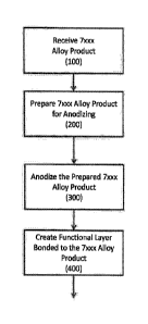
aluminum alloy products relating thereto. Referring now to FIGS. 1-2, a method
may
comprise an optional receiving step (100), wherein a 7xxx aluminum alloy
product (1) having
a 7xxx aluminum alloy base (10) with a surface oxide layer (20) thereon is
received. The
surface oxide layer (20) (sometimes referred to herein as the as-received
oxide layer)
generally has an as-received thickness, generally from 5 nm to 60 nm thick,
depending on its
temper. Products shipped in the W-temper or T-temper may have a thicker as-
received
thickness (e.g., from about 20 to 60 nanometer), whereas F-temper products may
have a
thinner as-received oxide thickness (e.g., from about 5 to 20 nanometers).
While the surface
oxide layer (20) is illustrated as being generally uniform, the surface oxide
layer generally
has a non-uniform topography.
[003] Still referring to FIGS. 1-2, the 7xxx aluminum alloy product (1) may be
prepared
(200) for anodizing. The preparing step (200) generally comprises reducing the
thickness of
and/or eliminating the as-received surface oxide layer (20). The preparing
step (200) may
also remove a small portion of the top layer of the 7xxx aluminum alloy base
(e.g., a few
nanometers) and/or may remove any intermetallic particles (e.g., dominant
copper-bearing
intermetallic particles, such as Al7Cu2Fe particles) contained in the as-
received 7xxx
aluminum alloy product. Upon conclusion of the preparing step (200), the 7xxx
aluminum
alloy product generally comprises a prepared oxide layer (30) (FIG. 4). This
prepared oxide
layer (30) is thinner than the as-received oxide layer (20), generally having
an average
(mean) thickness of about 5-10 nanometers thick, or thereabouts. The prepared
oxide layer
(30) also generally comprises a non-uniform (e.g., scalloped) topography. This
prepared
oxide layer (30) generally facilitates the subsequent anodizing (300) and
creating a functional
layer (400) steps.
1
CA 03052308 2019-07-31
WO 2018/165053 PCT/US2018/020979
[004] In one embodiment, and referring now to FIGS. 3-4, the preparing step
(200) includes
a cleaning step (210) and an oxide removal step (220). When employed, the
cleaning step
(210) generally includes contacting the 7xxx aluminum alloy product with a
proper solvent
(e.g., an organic solvent, such as acetone or hexane) followed by an alkaline
or acid clean.
This cleaning step facilitates removal of debris, lubricant(s) and other items
on the surface of
the as-received 7xxx aluminum alloy product that might inhibit or disrupt the
subsequent
oxide removal step (220). In one embodiment, after application of the solvent,
the surface is
rinsed and then exposed to an alkaline cleaner, until the surface is "water-
break free" (e.g., is
uniformly wetted by water, such as when a contact angle of zero (0) degrees is
achieved
and/or when a surface tension of at least 0.072 N/m is achieved).
[005] After the cleaning step (210), the 7xxx aluminum alloy product is
generally subjected
to an oxide removal step (220), which thins and/or removes the oxide layer
(20) The oxide
removal step (220) may comprise, for instance, exposing the cleaned 7xxx
aluminum alloy
surface to a caustic solution (e.g., NaOH), then rinsing, then exposing the
7xxx aluminum
alloy surface to an acidic solution (e.g., nitric acid), and then rinsing
again. Other types of
oxide thinning methodologies may be employed. After the oxide removal step
(220), little or
none of the as-received surface oxide layer is present on the 7xxx aluminum
alloy body
surface. After the oxide thinning, the 7xxx aluminum alloy product generally
comprises a
prepared oxide layer (30). This prepared oxide layer (30) is thinner than the
as-received
oxide layer (20), generally having an average (mean) thickness of about 5-10
nanometers, or
thereabouts. The prepared oxide layer (30) also generally comprises a non-
uniform (e.g.,
scalloped) topography. This prepared oxide layer generally (30) facilitates
the subsequent
anodizing (300) and creating a functional layer (400) steps.
[006] Referring now to FIGS. 5-6, after the preparing step (200), the prepared
7xxx
aluminum alloy body is subjected to a short anodizing step to produce a thin
anodic oxide
layer (40) on the prepared oxide layer (30) created as a result of the
preparing step (200).
The anodizing step (300) is generally a single-step anodizing, and generally
comprises
exposing the prepared 7xxx aluminum alloy body prepared in step (200) to
anodizing
conditions sufficient to produce (e.g., grow) the thin anodic oxide layer (40)
on top of the
prepared oxide layer (30). A single-step anodizing is where generally the same
anodizing
conditions are used throughout the anodizing, resulting in the production of a
single,
generally homogeneous, anodic oxide layer. The anodic oxide layer (40)
generally comprises
a near stoichiometric film of A1203 located on the surface of the prepared
oxide layer (30). In
2
one embodiment, the thin anodic oxide layer (40) has a thickness of from 10 to
145 nanometers.
After the anodizing, the 7xxx aluminum alloy product may be rinsed with water.
[007] The thickness of the anodic oxide layer (40) may be measured by XPS (X-
ray
Photoelectron Spectroscopy) using a sputter rate relative to an aluminum oxide
standard
having a verified oxide thickness. For instance, the oxide thickness may be
determined based
on a sputter rate relative to a measured thickness of A1203 that was
determined using a
commercially available SiO2 sputter-rate standard, which may have a known
thickness of 50
nm or 100 nm, for instance. The aluminum oxide standard material may be an
A1203 layer
that was deposited via e-beam evaporation onto a silicon wafer, and may have a
corresponding thickness of 50 nm or 100 nm, for instance. The relative ratio
of the
Si02/A1203 sputtering is approximately 1.6.
[008] The anodizing conditions used to produce the thin anodic oxide layer
(40) may vary
depending on the acidic electrolyte solution used. In one embodiment, the
acidic electrolyte
solution comprises one of sulfuric acid, phosphoric acid, chromic acid, and
oxalic acid. In
one embodiment, the anodizing solution consists essentially of sulfuric acid
(e.g., is
essentially a 10-20 wt. % sulfuric acid solution). In another embodiment, the
anodizing
solution consist essentially of phosphoric acid (e.g., is essentially a 5-20
wt. % phosphoric
acid solution). In yet another embodiment, the anodizing solution consist
essentially of
chromic acid. In another embodiment, the anodizing solution consist
essentially of oxalic
acid. In one embodiment, the anodizing solution has a temperature of from 60
to 100 F
during anodizing. In one embodiment, the anodizing solution has a temperature
of at least
65 F during anodizing. In another embodiment, the anodizing solution has a
temperature of at
least 70 F during anodizing. In one embodiment, the anodizing solution has a
temperature of
not greater than 95 F during anodizing. In another embodiment, the anodizing
solution has a
temperature of not greater than 90 F during anodizing.
[009] After the anodizing step (300), the combined thickness of the prepared
oxide layer
(30) and the anodic oxide layer (40) should be at least 15 nanometers thick,
but not greater
than 150 nanometers thick (i.e., the combined thickness of layer (30) plus
layer (40) should
be from 15-150 nanometers). As described in further detail below, in step
(400), a
functionalized layer is created after the anodizing step (300). This creating
step (400)
includes exposing the anodized 7xxx aluminum alloy product to an appropriate
phosphorous-
containing organic acid (e.g., an organophosphoric or an organophosphonic
acid). If the
combined thickness of the prepared oxide layer (30) and the anodic oxide layer
(40) is less
3
6861490
Date Recue/Date Received 2021-08-27
CA 03052308 2019-07-31
WO 2018/165053 PCT/US2018/020979
than 15 nanometers thick, then insufficient penetration of phosphorous may
occur in the
creating step (400). If the combined thickness of the prepared oxide layer
(30) and the anodic
oxide layer (40) is more than 150 nanometers thick, then adhesive bonding
performance
(after the creating step (400)) may be degraded.
[0010] In one embodiment, the combined thickness of the prepared oxide layer
(30) and the
anodic oxide layer (40) is at least 20 nanometers. In another embodiment, the
combined
thickness of the prepared oxide layer (30) and the anodic oxide layer (40) is
at least 25
nanometers. In one embodiment, the combined thickness of the prepared oxide
layer (30)
and the anodic oxide layer (40) is not greater than 135 nanometers thick. In
another
embodiment, the combined thickness of the prepared oxide layer (30) and the
anodic oxide
layer (40) is not greater than 125 nanometers thick. In yet another
embodiment, the
combined thickness of the prepared oxide layer (30) and the anodic oxide layer
(40) is not
greater than 115 nanometers thick. In another embodiment, the combined
thickness of the
prepared oxide layer (30) and the anodic oxide layer (40) is not greater than
105 nanometers
thick. In yet another embodiment, the combined thickness of the prepared oxide
layer (30)
and the anodic oxide layer (40) is not greater than 100 nanometers thick. In
another
embodiment, the combined thickness of the prepared oxide layer (30) and the
anodic oxide
layer (40) is not greater than 95 nanometers thick. In yet another embodiment,
the combined
thickness of the prepared oxide layer (30) and the anodic oxide layer (40) is
not greater than
90 nanometers thick. In another embodiment, the combined thickness of the
prepared oxide
layer (30) and the anodic oxide layer (40) is not greater than 85 nanometers
thick. In yet
another embodiment, the combined thickness of the prepared oxide layer (30)
and the anodic
oxide layer (40) is not greater than 80 nanometers thick. In another
embodiment, the
combined thickness of the prepared oxide layer (30) and the anodic oxide layer
(40) is not
greater than 75 nanometers thick. In yet another embodiment, the combined
thickness of the
prepared oxide layer (30) and the anodic oxide layer (40) is not greater than
70 nanometers
thick. In another embodiment, the combined thickness of the prepared oxide
layer (30) and
the anodic oxide layer (40) is not greater than 65 nanometers thick, or
thinner.
[0011] Still referring to FIGS. 5-6, in one embodiment, the anodizing step
(300) comprises
anodizing in an appropriate acidic solution (e.g., sulfuric acid) for a time
sufficient and under
conditions sufficient to create the anodic oxide layer (40). In one approach,
the current
density is from 5-20 amperes per square foot (ASF), and the anodizing time is
not greater
than 120 seconds, depending on the current density employed. In one
embodiment, the
4
CA 03052308 2019-07-31
WO 2018/165053 PCT/US2018/020979
anodizing comprises anodizing in sulfuric acid (e.g., a 10-20 wt. % sulfuric
acid solution), at
room temperature, and at 15 ASF for 10 to 40 seconds, or similar conditions,
as required to
facilitate production of the anodic oxide layer of suitable thickness. In
another embodiment,
the anodizing comprises anodizing in sulfuric acid, at room temperature, at 12
ASF for 10 to
60 seconds. In another embodiment, the anodizing comprises anodizing in
sulfuric acid, at
room temperature, at 6 ASF for 10 to 60 seconds. In one embodiment, the
sulfuric acid
solution has a concentration of 12-18 wt. % sulfuric acid. In another
embodiment, the
sulfuric acid solution has a concentration of 14-16 wt. % sulfuric acid. In
another
embodiment, the sulfuric acid solution is an about 15 wt. % sulfuric acid
solution. Other
appropriate sulfuric anodizing conditions can be used.
[0012] In another approach (not illustrated), the anodizing step (300)
comprises anodizing in
an appropriate phosphoric acid solution for a time sufficient and under
conditions sufficient
to create the anodic oxide layer (40). In one embodiment, the voltage applied
is from 10-20
volts, and the anodizing time is not greater than 120 seconds. In one
embodiment, the
anodizing comprises anodizing in phosphoric acid (e.g., a 5-20 wt. %
phosphoric acid
solution) having a temperature of from 80-100 F (e.g., 90 F) and at 13-18
volts for 10 to 60
seconds, or similar conditions, as required to facilitate production of the
anodic oxide layer of
suitable thickness. Other appropriate phosphoric anodizing conditions can be
used.
[0013] After the anodizing step (300) and any appropriate intervening steps
(e.g., rinsing),
the method may include creating a functional layer (400) via an appropriate
chemical (e.g., a
phosphorus-containing organic acid). In one embodiment, the creating step
(400) may
include contacting the anodized 7xxx aluminum alloy product with any of the
phosphorus-
containing organic acids disclosed in U.S. Patent No. 6,167,609 to Marinelli
et al., which is
incorporated herein by reference. A layer of polymeric adhesive may then be
applied to the
functionalized layer (e.g., for joining to a metal support structure to form a
vehicle assembly).
The creating step (400) may alternatively use conversion coatings in lieu of a
phosphoric
containing organic acid. For instance, conversion coatings employing titanium
or titanium
with zirconium may be used. Thus, in one embodiment, after anodizing, the
anodic oxide
layer is contacted with a Ti-type or TiZr-type conversion coating to create
the
functionalization layer.
[0014] Prior to creating the functional layer (400), the prepared 7xxx
aluminum alloy product
may be further prepared, such as by rinsing the prepared 7xxx aluminum alloy
product. To
create the functional layer, the prepared 7xxx aluminum alloy product is
generally exposed to
CA 03052308 2019-07-31
WO 2018/165053 PCT/US2018/020979
an appropriate chemical, such as an acid or base. In one embodiment, the
chemical is a
phosphorous-containing organic acid. The organic acid generally interacts with
aluminum
oxide in the prepared oxide layer to form a functionalized layer. The organic
acid is dissolved
in water, methanol, or other suitable organic solvent, to form a solution that
is applied to the
7xxx aluminum alloy product by spraying, immersion, roll coating, or any
combination
thereof. The phosphorus-containing organic acid may be an organophosphonic
acid or an
organophosphinic acid. The pretreated body is then rinsed with water after the
acid
application step. In another embodiment, the chemical is a Ti-type or TiZr-
type conversion
coating.
[0015] The term "organophosphonic acid" includes acids having the formula
Rin[P0(01-1)7]
wherein R is an organic group containing 1-30 carbon atoms, m is the number of
organic
groups and is about 1-10, and n is the number of phosphonic acid groups and is
about 1-10.
Some suitable organophosphonic acids include vinyl phosphonic acid,
methylphosphonic
acid, ethylphosphonic acid, octylphosphonic acid and styrenephosphonic acid
[0016] The term "organophosphinic acid" includes acids having the formula
Rõ,R10[PO(OH)]n
wherein R is an organic group containing 1-30 carbon atoms, R' is hydrogen or
an organic
group containing 1-30 carbon atoms, m is the number of R groups and is about 1-
10, n is the
number of phosphinic acid groups and is about 1-10, and o is the number of R'
groups and is
about 1-10. Some suitable organophosphinic acids include phenylphosphinic acid
and bis-
(perfluoroheptyl)phosphinic acid.
[0017] In one embodiment, a vinyl phosphonic acid surface treatment is used
that forms
essentially a monolayer with aluminum oxide in the surface layer. The coating
areal weight
may be less than about 15 mg/m2. In one embodiment, the coating areal weight
is only about
3 mg/m2.
[0018] An advantage of these phosphorus-containing organic acids is that the
pretreatment
solution contains less than about 1 wt. % chromium and preferably essentially
no chromium.
Accordingly, environmental concerns associated with chromate conversion
coatings are
eliminated
[0019] Due to the functionalization, the anodic oxide layer (40) may include
phosphorous. In
one embodiment, a surface phosphorous content of the anodic oxide layer is at
least 0.2
mg/m2 (average). As used herein, "surface phosphorus content" means the
average amount
of phosphorus at the surface of the anodic oxide layer (40) as measured by XRF
(X-Ray
Fluorescence). The area of collection should be at least 3 cm x 3 cm (1.25
inches by 1.25
6
CA 03052308 2019-07-31
WO 2018/165053 PCT/US2018/020979
inches) across the functionalized surface. In one embodiment, a surface
phosphorous content
of the anodic oxide layer is at least 0.3 mg/m2 (average). In another
embodiment, a surface
phosphorous content of the anodic oxide layer is at least 0.4 mg/m2 (average).
In yet another
embodiment, a surface phosphorous content of the anodic oxide layer is at
least 0.5 mg/m2
(average). In another embodiment, a surface phosphorous content of the anodic
oxide layer is
at least 0.6 mg/m2 (average). In yet another embodiment, a surface phosphorous
content of
the anodic oxide layer is at least 0.7 mg/m2 (average). The surface
phosphorous content of
the anodic oxide layer is generally not greater than 4.65 mg/m2 (average).
[0020] When the functionalization solution is a phosphorous-containing organic
acid, the
functionalization generally results in the phosphorus being bound to an
organic group (R) as
shown in FIG. 8a. In one embodiment, the organic group (R) comprises a vinyl
group. Such
organic binding does not occur with phosphoric acid anodizing, which generally
produces P-
O bonds, as shown in FIGS. 8b-8c. In one embodiment, the anodic oxide layer
(40)
comprises a phosphorous concentration gradient, as measured by XPS (X-Ray
Photoelectron
Spectroscopy), wherein the amount of phosphorous at the surface of the anodic
oxide layer
(within 10 nm of the surface) ("P-surface") exceeds the amount of phosphorous
at the
interface ("P-interface") between the anodic oxide layer (40) and the prepared
oxide layer
(30). In one embodiment, the P-surface concentration, by atomic percent, is at
least 10%
higher than the P-interface concentration. In
another embodiment, the P-surface
concentration, by atomic percent, is at least 25% higher than the P-interface
concentration.
[0021] The functionalized 7xxx aluminum alloy product may be cut in desired
sizes and
shapes and/or worked into a predetermined configuration. Castings, extrusions
and plate may
also require sizing, for example by machining, grinding or other milling
process, and prior to
the application of the methods described herein. Shaped assemblies made in
accordance with
the invention are suitable for many components of vehicles, including
automotive bodies,
body-in-white components, doors, trunk decks and hood lids. The functionalized
7xxx
aluminum alloy products may be bonded to a metal support structure using a
polymeric
adhesive.
[0022] In manufacturing automotive components, it is often necessary to join
the
functionalized 7xxx aluminum alloy material to an adjacent structural member.
Joining
functionalized 7xxx aluminum alloy materials may be accomplished in two steps.
First, a
polymeric adhesive layer may be applied to the functionalized 7xxx aluminum
alloy product,
after which it is pressed against or into another component (e.g., another
functionalized 7xxx
7
CA 03052308 2019-07-31
WO 2018/165053 PCT/US2018/020979
aluminum alloy product; a steel product; a 6xxx aluminum alloy product; a 5xxx
aluminum
alloy product; a carbon reinforced composite). The polymeric adhesive may be
an epoxy, a
polyurethane or an acrylic.
[0023] After the adhesive is applied, the components may be spot welded
together, e.g., in a
joint area of applied adhesive. Spot welding may increase peel strength of the
assembly and
may facilitate handling during the time interval before the adhesive is
completely cured. If
desired, curing of the adhesive may be accelerated by heating the assembly to
an elevated
temperature. The assembly may then be passed through a paint preparation
process (e.g., a
zinc phosphate bath or zirconium based treatment), dried, electrocoated, and
subsequently
painted with an appropriate finish.
[0024] Referring now to FIG. 7, in one embodiment, after the creating step
(400), the method
includes bonding (702) at least a portion of the functionalized 7xxx aluminum
alloy product
with a "second material," thereby creating an as-bonded 7xxx aluminum alloy
product. In
one embodiment, the bonding (702) step may include curing (not illustrated)
the adhesive
bonding agent applied (704) to the at least a portion of the functionalized
7xxx aluminum
alloy product and/or the at least a portion of the second material for a
predetermined amount
of time and/or at a predeteimined temperature. The curing step may be
performed
concomitant to or after the applying step (704). In one embodiment, the as-
bonded 7xxx
aluminum alloy product may include the first portion of the 7xxx aluminum
alloy product
adhesively structurally bonded to the second material via the applied (704)
and/or cured
adhesive bonding agent. In one embodiment, at least a portion of the
functionalized 7xxx
aluminum alloy product includes a first portion of the functionalized 7xxx
aluminum alloy
product, and the second material includes at least a second portion of the
functionalized 7xxx
aluminum alloy product.
[0025] As used in the context of FIG. 7 and its above description, "second
material" means a
material to which at least a portion of an aluminum alloy product is bonded,
thereby forming
an as-bonded aluminum alloy product
[0026] In one embodiment of the method, when the as-bonded 7xxx aluminum alloy
product
is in the form of a single-lap-joint specimen having an aluminum metal-to-
second material
joint overlap of 0.5 inches, the as-bonded 7xxx aluminum alloy product
achieves completion
of 45 stress durability test (SDT) cycles according to ASTM D1002 (10). In one
embodiment, a residual shear strength of the single-lap-joint specimen after
completing the
45 SDT cycles is at least 80% of an initial shear strength. In another
embodiment, the
8
CA 03052308 2019-07-31
WO 2018/165053 PCT/US2018/020979
residual shear strength of the single-lap-joint specimen after completing the
45 SDT cycles is
at least 85% of the initial shear strength. In yet another embodiment, the
residual shear
strength of the single-lap-joint specimen after completing the 45 SDT cycles
is at least 90%
of the initial shear strength.
[0027] The method may optionally comprise one or more thermal exposure steps.
For
instance, purposeful thermal exposure steps may be applied before the
preparing step (200),
before the anodizing step (300), and/or after the creating step (400). The
thermal exposure
step(s) may result in the production of a thermal oxide layer on the 7xxx
aluminum alloy
product. In one embodiment, the total thickness of the prepared oxide layer
plus the thermal
oxide layer plus the anodic oxide layer is from 15-150 nanometers, as
described above
relative to FIGS. 5-6 and for the same reasons (e.g., to facilitate subsequent
adhesive
bonding).
[0028] In one embodiment, the total thickness of the prepared oxide layer plus
the thermal
oxide layer plus the anodic oxide layer is at least 20 nanometers. In another
embodiment, the
total thickness of the prepared oxide layer plus the thermal oxide layer plus
the anodic oxide
layer is at least 25 nanometers. In one embodiment, the total thickness of the
prepared oxide
layer plus the thermal oxide layer plus the anodic oxide layer is not greater
than 135
nanometers thick. In another embodiment, the total thickness of the prepared
oxide layer plus
the thermal oxide layer plus the anodic oxide layer is not greater than 125
nanometers thick.
In yet another embodiment, the total thickness of the prepared oxide layer
plus the thermal
oxide layer plus the anodic oxide layer is not greater than 115 nanometers
thick. In another
embodiment, the total thickness of the prepared oxide layer plus the thermal
oxide layer plus
the anodic oxide layer is not greater than 105 nanometers thick. In yet
another embodiment,
the total thickness of the prepared oxide layer plus the themial oxide layer
plus the anodic
oxide layer is not greater than 100 nanometers thick. In another embodiment,
the total
thickness of the prepared oxide layer plus the thermal oxide layer plus the
anodic oxide layer
is not greater than 95 nanometers thick. In yet another embodiment, the total
thickness of the
prepared oxide layer plus the thermal oxide layer plus the anodic oxide layer
is not greater
than 90 nanometers thick. In another embodiment, the total thickness of the
prepared oxide
layer plus the thermal oxide layer plus the anodic oxide layer is not greater
than 85
nanometers thick. In yet another embodiment, the total thickness of the
prepared oxide layer
plus the thermal oxide layer plus the anodic oxide layer is not greater than
80 nanometers
thick. In another embodiment, the total thickness of the prepared oxide layer
plus the thermal
9
CA 03052308 2019-07-31
WO 2018/165053 PCT/US2018/020979
oxide layer plus the anodic oxide layer is not greater than 75 nanometers
thick. In yet another
embodiment, the total thickness of the prepared oxide layer plus the thermal
oxide layer plus
the anodic oxide layer is not greater than 70 nanometers thick. In another
embodiment, the
total thickness of the prepared oxide layer plus the thermal oxide layer plus
the anodic oxide
layer is not greater than 65 nanometers thick, or thinner.
[0029] In one approach, a thermal exposure may be completed before the
preparing step
(200) (i.e., after the receiving step (100) and before the preparing step
(200)). In one
embodiment, a solution heat treatment and quench (a solutionizing treatment)
may be
completed on as received F-temper product, after which the preparing step
(200) is
completed. For instance, an as-received 7xxx aluminum alloy product may be in
the F-
temper (as fabricated). Prior to the preparing step (200), the 7xxx aluminum
alloy product
may be formed into a predetennined shaped product, such as an automotive
component (e.g.,
door outer and/or inner panels, body-in-white components (A-pillars, B-pillar,
or C-pillars),
hoods, deck lids, and similar components) This forming step may be completed
at elevated
temperatures, and may, therefore subject the 7xxx aluminum alloy product to
various thermal
practices (e.g., consistent with a solutionizing treatment (i.e., a solution
heat treatment plus
quench), when warm or hot forming and then die quenched). To further develop
the strength
(or other properties) of the formed 7xxx aluminum alloy product, the formed
7xxx aluminum
alloy product may be artificially aged, which artificial aging may occur
before the preparing
step (200), before the anodizing step (300), and/or after the creating step
(400). In one
embodiment, one or more artificial aging steps follow a solutionizing
treatment, after which
the preparing step (200) is completed. In another embodiment, artificial aging
is completed
on an as-received W-temper or T-temper product, after which the preparing step
(200) is
completed. Paint baking may then occur after the creating step (400).
[0030] In one approach, a thermal exposure may be completed before the
anodizing step
(200) (i.e., after the preparing step (100) and before the anodizing step
(200)). For instance, a
solution heat treatment and quench (a solutionizing treatment) may be
completed on a
prepared F-temper product, after which the anodizing step (200) is completed.
For instance,
an as-received 7xxx aluminum alloy product may be in the F-temper (as
fabricated). After
the preparing step (200) and prior to the anodizing step (300), the 7xxx
aluminum alloy
product may be fonned into a predetermined shaped product, such as an
automotive
component (e.g., door outer and/or inner panels, body-in-white components (A-
pillars, B-
pillar, or C-pillars), hoods, deck lids, and similar components). This forming
step may be
CA 03052308 2019-07-31
WO 2018/165053 PCT/US2018/020979
completed at elevated temperatures, and may, therefore subject the 7xxx
aluminum alloy
product to various thermal practices (e.g., consistent with a solutionizing
treatment (i.e., a
solution heat treatment plus quench), when warm or hot forming and then die
quenched). To
further develop the strength (or other properties) of the formed 7xxx aluminum
alloy product,
the formed 7xxx aluminum alloy product may be artificially aged, which
artificial aging may
occur before the anodizing step (300), and/or after the creating step (400).
[0031] In one embodiment, one or more artificial aging steps follow a
solutionizing
treatment, after which the anodizing step (300) is completed. In another
embodiment,
artificial aging is completed on an as-received W-temper or T-temper product,
after which the
preparing step (200) is completed. Paint baking may then occur after the
creating step (400)
[0032] Any of the thermal exposure steps described above may be combined, as
applicable,
to complete the product. For instance, a thermal exposure may be completed
both prior to
preparing (200) and prior to anodizing (300). Paint baking may then occur
after the creating
step (400)
[0033] When utilized, the artificial aging may facilitate realization of any
of an underaged,
peak aged, or overaged temper. As may be appreciated, the 7xxx aluminum alloy
product
may be formed before an artificial aging step, or after an artificial aging
step, if utilized.
[0034] The methods disclosed herein are generally applicable to 7xxx aluminum
alloy
products, such as those including copper resulting in the formation of copper-
bearing
intermetallic particles. In one approach, the 7xxx aluminum alloy product
comprises 2-12 wt.
% Zn, 1-3 wt. % Mg, and 0-3 wt. % Cu (e.g., 1-3 wt. ,70 Cu). In one
embodiment, the 7xxx
aluminum alloy product is one of a 7009, 7010, 7012, 7014, 7016, 7116, 7032,
7033, 7034,
7036, 7136, 7037, 7040, 7140, 7042, 7049, 7149, 7249, 7349, 7449, 7050, 7150,
7055, 7155,
7255, 7056, 7060, 7064, 7065, 7068, 7168, 7075, 7175, 7475, 7178, 7278, 7081,
7181, 7085,
7185, 7090, 7093, 7095, 7099, or 7199 aluminum alloy, as defined by the
Aluminum
Association Teal Sheets (2015). In one embodiment, the 7xxx aluminum alloy is
7075, 7175,
or 7475. In one embodiment, the 7xxx aluminum alloy is 7055, 7155, or 7225. In
one
embodiment, the 7xxx aluminum alloy is 7065. In one embodiment, the 7xxx
aluminum
alloy is 7085 or 7185. In one embodiment, the 7xxx aluminum alloy is 7050 or
7150. In one
embodiment, the 7xxx aluminum alloy is 7040 or 7140. In one embodiment, the
7xxx
aluminum alloy is 7081 or 7181. In one embodiment, the 7xxx aluminum alloy is
7178.
[0035] The 7xxx aluminum alloy product may be in any form, such as in the foim
of a
wrought product (e.g., a rolled sheet or plate product, an extrusion, a
forging). The 7xxx
11
CA 03052308 2019-07-31
WO 2018/165053 PCT/US2018/020979
aluminum alloy product may alternatively be in the form of a shape-cast
product (e.g., a die
casting). The 7xxx aluminum alloy product may alternatively be an additively
manufactured
product. As used herein, "additive manufacturing" means "a process of joining
materials to
make objects from 3D model data, usually layer upon layer, as opposed to
subtractive
manufacturing methodologies", as defined in ASTM F2792-12a entitled "Standard
Terminology for Additively Manufacturing Technologies".
[0036] The temper and 7xxx aluminum alloy definitions provided herein are per
ANSI H35.1
(2009).
BRIEF DESCRIPTION OF THE DRAWINGS
[0037] FIG. 1 is a cross-sectional schematic view of an 7xxx aluminum alloy
product (1)
(e.g., an as-received 7xxx aluminum alloy product) having a base (10) and
surface oxides
thereon (20) (not to scale; for illustration purposes only).
[0038] FIG 2 is a flow chart illustrating one embodiment of a method for
producing 7xxx
aluminum alloy products in accordance with the present disclosure.
[0039] FIG. 3 is a flow chart illustrating one embodiment of the preparing
step (200) of FIG.
2.
[0040] FIG. 4 is a cross-sectional schematic view of a prepared 7xxx aluminum
alloy product
(1) having a base (10) with prepared surface oxides (30) thereon (not to
scale; for illustration
purposes only).
[0041] FIG. 5 is a flow chart illustrating one embodiment of the anodizing
step (300) of FIG.
2.
[0042] FIG. 6 is a cross-sectional schematic view of a prepared and anodized
7xxx aluminum
alloy product (1) having a base (10) with prepared surface oxides (30) and
anodic oxides (40)
thereon (not to scale; for illustration purposes only).
[0043] FIG. 7 is a flow chart illustrating one embodiment of the creating step
(400) of FIG. 2.
[0044] FIG. 8A is a diagram illustrating a representative chemical bond
structure of an as-
functionalized 7xxx aluminum alloy product following the creating step (400)
of FIG. 2.
[0045] FIGS. 8B and 8C are diagrams illustrating chemical bond structures of a
phosphoric
acid anodizing 7xxx aluminum alloy product.
[0046] FIG. 9 is a plot of X-ray photoelectron spectroscopy (XPS) oxide
structure analysis
results of a 7xxx aluminum alloy product treated according to one embodiment
of the
disclosure.
12
CA 03052308 2019-07-31
WO 2018/165053 PCT/US2018/020979
[0047] FIG. 10 is a scanning electron micrograph (SEM) image of the surface
topography of
the 7xxx aluminum alloy product of FIG. 9.
DETAILED DESCRIPTION
[0048] Example 1
[0049] Several samples of a 7xxx aluminum alloy (Al-Zn-Mg-Cu style) product
were
received and prepared as per step (200) of FIG. 2, above. After the preparing
step (200) a
native oxide layer (4-6 nm thick) was present on the surface of the sample.
The 7xxx
aluminum alloy products were not anodized, but, instead, were simply subjected
to the
creating step (400), as per FIG. 2, and in accordance with U.S. Patent No.
6,167,609 to
Marinelli et al. After the creating step, the samples were sequentially bonded
and then
subjected to an industry standard cyclical corrosion exposure test, similar to
ASTM D1002,
which continuously exposes the samples to 1080 psi lap shear stresses to test
bond durability.
All samples failed to complete the required 45 cycles in the bond durability
test.
[0050] Example 2
[0051] Several samples of a 7xxx aluminum alloy (Al-Zn-Mg-Cu style) were
processed as
per FIG. 2. The alloys were all anodized in a 15 wt. % sulfuric acid solution
at 70 F and 6
ASF for 10, 45, or 60 seconds. After anodizing, a functional layer was then
created (400),
per FIG. 2 and in accordance with U.S. Patent No. 6,167,609 to Marinelli et
al., on each of
the materials, after which the materials were sequentially bonded and then
subjected to an
industry standard cyclical corrosion exposure test, similar to ASTM D1002.
[0052] The samples anodized for 60 seconds successfully completed the required
45 cycles
and produced retained lap shear strengths of 7253, 6600, 6851 and 7045 psi in
the four
replicate specimens (6937 psi, ave., with a stdev (a) of 278 psi). These
residual shear
strength results are superior to the typical range of 4500-6000 psi typically
observed for
adhesively bonded 5xxx and 6xxx alloys prepared by another conventional
industry practice.
The four residual shear strength results are also consistent, as indicated by
the low standard
deviation. The samples anodized for only 10 or 45 seconds at 6 ASF did not
successfully
complete the bond durability testing. Only two of the 45 second anodized
samples survived
the 45 cycles, and none of the 10 second anodized samples survived the 45
cycle
requirement.
[0053] As a baseline, four of the same alloy samples were prepared similarly
to above, but
were held for 60 seconds in the 15 wt. % sulfuric acid anodizing bath at 70 F,
without any
13
CA 03052308 2019-07-31
WO 2018/165053 PCT/US2018/020979
current applied. The same functional layer was then created (400), per FIG. 2
and in
accordance with U.S. Patent No. 6,167,609 to Marinelli et al., on each of the
materials, after
which the materials were sequentially bonded and then subjected to an industry
standard
cyclical corrosion exposure test, similar to ASTM D1002. All four samples
failed at either 2
or 3 cycles, confirming that the anodic oxide layer produced during
anodization facilitates
appropriate production of the functional layer and subsequent adhesive
bonding.
[0054] Example 3
[0055] Several samples of a 7xxx aluminum alloy (Al-Zn-Mg-Cu style) were
processed as
per FIG. 2. The alloys were all anodized in a 15 wt. A sulfuric acid solution
at 70 F and 15
ASF for 10, 20, 30, or 40 seconds. After anodizing, a functional layer was
then created
(400), per FIG. 2 and in accordance with U.S. Patent No. 6,167,609 to
Marinelli et al., on
each of the materials, after which the materials were sequentially bonded and
then subjected
to an industry standard cyclical corrosion exposure test, similar to ASTM
D1002. All four
anodizing conditions resulted in the specimens completing the required 45
cycles, and with
retained strength levels of from 3512 to 6519 psi. The average retained
strengths were 5698
psi (stdev (a) of 205 psi) (40 sec.), 5091 psi (30 sec.), 5665 psi (20 sec.),
and 5167 psi (10
sec.). The higher current density (as compared to Example 2) facilitated
production of an
anodic oxide layer having an appropriate thickness for facilitating the
creating step (400) and
subsequent adhesive bonding.
[0056] To verify oxide thickness, one of the 10 second anodized samples was
analyzed by
XPS. The analysis indicated that the anodic oxide layer had a thickness of 28
nm thick, and
consisted essentially of aluminum oxides (e.g., A1203). See, FIG. 9. The
surface of the oxide
also includes a plurality of pits. See, FIG. 10. It is believed that these
pits may at least assist
in facilitating approved adhesive boding performance for the 7xxx aluminum
alloy products.
[0057] As per Example 2, baseline samples were also prepared using the same
conditions as
the anodized sample, but in the absence of anodizing¨the samples, instead,
were placed in
the 15 wt. % sulfuric acid anodizing bath at 70 F without any current applied.
The same
functional layer was then created (400), per FIG. 2 and in accordance with
U.S. Patent No.
6,167,609 to Marinelli et al., on each of the materials, after which the
materials were
sequentially bonded and then subjected to an industry standard cyclical
corrosion exposure
test, similar to ASTM D1002. All samples failed within a few cycles (3-6),
again confirming
14
CA 03052308 2019-07-31
WO 2018/165053 PCT/US2018/020979
that the anodic oxide layer produced during anodization facilitates
appropriate production of
the functional layer and subsequent adhesive bonding.
[0058] To confirm that different anodizing conditions could be used with this
same material,
one additional sample of the material was prepared as per FIG. 2. The alloy
was also
anodized in a 15 wt. % sulfuric acid at 70 F, but at 6 ASF for 20 seconds. The
same
functional layer was then created (400), per FIG. 2 and in accordance with
U.S. Patent No.
6,167,609 to Marinelli et al., on each of the specimens, after which the
materials were
sequentially bonded and then subjected to an industry standard cyclical
corrosion exposure
test, similar to ASTM D1002. These specimens all completed the required 45
cycles, and
with an average retained strength of 5032 psi.
[0059] Example 4
[0060] Several additional 7xxx aluminum alloys (Al-Zn-Mg-Cu style) were
processed as per
FIG. 2. The alloys were all anodized in a 15 wt. % sulfuric acid solution at
70 F and 12 ASF
for 20, 40, or 60 seconds. After anodizing, a functional layer was then
created (400), per
FIG. 2 and in accordance with U.S. Patent No. 6,167,609 to Marinelli et al.,
on each of the
materials, after which the materials were sequentially bonded and then
subjected to an
industry standard cyclical corrosion exposure test, similar to ASTM D1002. In
this example,
the specimens anodized for 40 second and 60 second did not pass the testing ---
there was just
one "survivor" out of each of the four specimens at each condition. However,
in the set
anodized for 20 seconds, three of the four specimens completed the required 45
cycles and
produced retained shear strengths of 3765, 5294 and 6385 psi. The fourth
specimen survived
44 of the 45 cycles, but failed at the 45th cycle.
[0061] The anodic oxide layers of the 20 second and 40 second anodized sample
were then
analyzed by XPS. The 20 second anodized sample had an anodic oxide thickness
of 72 nm,
whereas the 40 second anodized sample has an anodic oxide thickness of 158 nm.
These
results indicate that the anodic oxide thickness must be maintained "thin" to
facilitate
subsequent functional layer preparation and adhesive bonding.
[0062] Example 5
[0063] Several additional samples of a 7xxx aluminum alloy (Al-Zn-Mg-Cu style)
were
processed as per FIG. 2, except the alloys were anodized in a 10 wt. %
phosphoric acid
solution at 90 F and 17.5V for 10 seconds. After anodizing, a functional layer
was then
CA 03052308 2019-07-31
WO 2018/165053 PCT/US2018/020979
created (400), per FIG. 2 and in accordance with U.S. Patent No. 6,167,609 to
Marinelli et
al., on each of the materials, after which the materials were sequentially
bonded and then
subjected to an industry standard cyclical corrosion exposure test, similar to
ASTM D1002.
In this example, three out of four of the samples completed the required 45
cycles and
produced retained shear strengths of 6011, 5932, and 5596, with an average of
5846 psi
(stdev (a) of 220 psi), showing the efficacy of the treatment using phosphoric
acid anodizing.
[0064] Without being bound to any particular theory, it is believed that the
functionalization
creates bonds between organic compounds and phosphorous in the anodic oxide
layer, an
example of which is FIG. 8a, wherein phosphorus atoms present in the
functionalized layer
covalently bond to an organic (R) group, in addition to being covalently
bonded to oxygen
atoms of the aluminum oxide. The "R groups" in the functionalized layer are
generally
organic groups containing 1-30 carbon atoms and/or hydrogen (i.e., R'),
depending on the
particular composition of the phosphorus-containing organic acid used during
the creating
(400) step. Phosphoric anodizing does not create such P-R boding. Instead,
phosphoric
anodizing generally creates P-0 bonding, as illustrated in FIGS. 8b-8c. The
identity of the
chemical structures associated with phosphorus provides the ability to readily
distinguish
(e.g., using analytical methods such as Fourier-transform infra-red (FTIR)
spectroscopy)
between anodized and functionalized 7xxx aluminum alloy products (including,
without
limitation, 7xxx aluminum alloy products), as well as to characterize the
compositions of the
chemicals used for the various treatment steps and the degree to and
conditions at which such
steps have been completed.
[0065] Whereas particular embodiments of this invention have been described
above for
purposes of illustration, it will be evident to those skilled in the art that
numerous variations
of the details of the present invention may be made without departing from the
invention as
defined in the appending claims.
16