Note: Descriptions are shown in the official language in which they were submitted.
CA 03052751 2019-08-06
WO 2018/146618 PCT/IB2018/050790
METHOD OF FINISHING A METALLIC CONDUCTIVE LAYER
Field
This application relates to finishing a metallic conductive layer, in
particular to
methods of finishing a metallic conductive layer comprising a solderable metal
for use in
.. printed circuits, and to methods of soldering on the metallic conductive
layer particularly
in the production of printed circuits.
Background
Copper layers located on top and bottom sides of printed circuit boards (PCBs)
oxidizes rapidly and the CuO/Cu02 oxides produced on the surface inhibit the
wetting
action of solder on the copper pad. This phenomenon renders the copper solder
layers
unsuitable for electronics components assembly due to its inability to produce
acceptable
and reliable solder joints. The copper therefore requires a surface finish in
order to render
the PCB usable. The surface finish has two essential functions: first to
protect the
exposed copper from oxidation; and, second to provide a solderable surface
when
assembling (soldering) components to the printed circuit board. Several PCB
surface
finishes exist and vary in price, availability, shelf life, reliability and
assembly processing.
While each finish has its own benefits and limitations, in most cases the
printed circuit
board design, the field of application (medical, military, aerospace,
industrial or other), the
environmental exposure and the assembly processes will dictate the surface
finish that is
.. the most appropriate for the application.
For example, the copper top and bottom solder layers of a PCB can be protected
from oxidation using Immersion tin or immersion silver processes. Silver
immersion in
particular is a process that offers good performance and superior surface
finishes. In a
silver immersion process, silver metal is selectively deposited on the copper
surfaces that
will need to be soldered and protected from oxidation and corrosion. Silver
immersion
yields a smooth uniform deposit on the copper that is approximately 8-15 pm
thick. A
surface finish having a flat topography is absolutely required to solder high
density
circuitry, like fine pitch ICs, high I/O BGAs, and very small electronics
components. Also,
immersion silver surface finish yield to acceptable PCB shelf-life of 6 months
to 12
.. months depending on the PCBs storage conditions.
Actual silver immersion surface finishes are electrodeposited or electroless-
plated
onto exposed copper surfaces using silver ions or silver salts solutions. From
a
manufacturing standpoint, the process is very sensitive to silver salt
concentration,
1
CA 03052751 2019-08-06
WO 2018/146618 PCT/IB2018/050790
solution PH, and requires automated process controls and measurements to
maintain the
deposition rate and the surface finish quality. The immersion silver process
steps are
plating of the board in tanks of agitated acidic solutions, followed by
sonication and
cleaning of the resulting PCB. Sulfur contamination, which is detrimental to
forming a
good solder joint, can occur during these steps. Another issue inherent to the
actual
process is that it uses a lot of water, generates toxic wastes and
necessitates water
decontamination facilities to treat the process effluents. Finally, employees
working in
these facilities must wear protection equipment for their safety.
Considering all the above, there is a need for an additive method that enables
the
formation of a silver surface finish that both protects a conductive metallic
layer and
allows soldering using lead and lead-free solders. Such an additive process
would be a
cost-effective method of finishing a solderable metal with silver.
Summary
In one aspect, there is provided a process for finishing a conductive metallic
layer,
the process comprising: coating a molecular silver ink on a conductive
metallic layer, the
molecular silver ink comprising a silver carboxylate, a carrier and a
polymeric binder; and,
decomposing the silver ink to form a solderable coating of silver metal on the
conductive
metallic layer.
In another aspect, there is provided a process for soldering on a conductive
.. metallic layer, the process comprising: coating a molecular silver ink on a
conductive
metallic layer, the molecular silver ink comprising a silver carboxylate, a
carrier and a
polymeric binder; decomposing the silver ink to form a solderable coating of
silver metal
on the conductive metallic layer; and, applying a solder to the solderable
silver metal
coated on the conductive metallic layer to form a solder joint with the silver
metal.
In another aspect, there is provided a layered material comprising a
conductive
metallic layer deposited on at least a portion of a surface of a substrate,
the conductive
metallic layer at least partially coated with a molecular ink comprising a
silver carboxylate,
a carrier, and a polymeric binder, the polymeric binder comprising a
polyester, polyimide,
polyether imide or any mixture thereof having functional groups that render
the polymeric
binder compatible with the carrier.
In another aspect, there is provided a use of a hydroxyl- and/or carboxyl-
terminated polyester as a binder in a molecular ink.
2
CA 03052751 2019-08-06
WO 2018/146618 PCT/IB2018/050790
The processes are additive and enable the formation of a silver metal finish
on a
conductive metallic layer, which both protects the conductive metallic layer
and allows
soldering with lead and lead-free solders. The process is cost-effective.
Further features will be described or will become apparent in the course of
the
following detailed description. It should be understood that each feature
described herein
may be utilized in any combination with any one or more of the other described
features,
and that each feature does not necessarily rely on the presence of another
feature except
where evident to one of skill in the art.
Brief Description of the Drawings
For clearer understanding, preferred embodiments will now be described in
detail
by way of example, with reference to the accompanying drawings, in which:
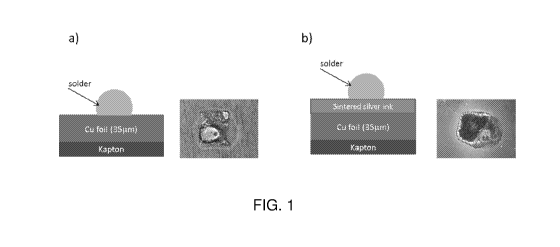
Fig. 1A depicts a schematic diagram (left) and an optical image (right) of a
silver-
coated copper surface on which a solder has been applied. The silver coating
was formed
by printing a molecular silver ink on the copper surface followed by
sintering. The silver
coating allows the formation of a stable and strong solder joint.
Fig. 1B depicts a schematic diagram (left) and an optical image (right) of a
bare
copper surface on which a solder has been applied. The solder does not wet the
copper
surface properly resulting in a solder joint unacceptable as per IPC A-610.
Fig 2A shows a cross-sectional SEM image showing the intermetallic layer
between the solder and copper foil with a silver finish solder
Fig 2B and 20 show cross-sectional SEM images with EDS analysis of the atomic
composition along the layer of solder, the intermetallic layer and copper
foil.
Detailed Description
The conductive metallic layer to be finished, or finished and soldered, may be
in
any physical form, for example as a free-standing structure such as a sheet
(e.g. foil,
plate), a wire, a sphere (e.g. ball bearing) and the like, or as a structure
deposited on a
substrate such as a thin sheet, a trace, a pillar, and the like deposited on
at least a
portion of a substrate. In the fabrication of printed circuit boards (PCBs) or
other
electronic structures, conductive metallic layer may be deposited on a
suitable substrate,
3
CA 03052751 2019-08-06
WO 2018/146618 PCT/IB2018/050790
often in the form of a trace. The conductive metallic layer may comprise a
solderable
metal, for example copper, gold, tin, palladium, aluminum or alloys thereof.
The process
is particularly useful for copper or copper alloys.
Suitable substrates may include, for example polyethylene terephthalate (PET)
(e.g. MelinexTm), polyolefin (e.g. silica-filled polyolefin (Teslin n")),
polydimethylsiloxane
(PDMS), polystyrene, acrylonitrile/butadiene/styrene, polycarbonate, polyimide
(e.g.
KaptonTm), thermoplastic polyurethane (TPU), silicone membranes, wool, silk,
cotton,
flax, jute, modal, bamboo, nylon, polyester, acrylic, aramid, spandex,
polylactide, paper,
glass, metal, dielectric coatings, among others.
Deposition of the conductive metallic layer on the substrate may be achieved
by
any suitable method, for example, electrodeposition (e.g. electroplating),
deposition and
sintering of molecular inks. Rigid and flex circuits are mainly manufactured
using a pure
metal foil laminated on a surface with the use of an adhesive and heat
followed by
etching to produce the traces and patterns needed.
When the conductive metallic layer is deposited or laminated on a rigid or
flexible
substrate, a layered material comprising a layer of solderable metal on at
least a portion
of a surface of the substrate may be produced. The conductive metallic layer
is preferably
fully coated with the molecular silver ink because IPC A-610 standards require
no
exposed copper on a rigid or flex circuit to prevent corrosion.
The ink may be coated on the conductive metal layer by any suitable method,
for
example printing. Printing methods may include, for example, screen printing,
stencilling,
inkjet printing, flexography printing, gravure printing, off-set printing,
stamp printing,
airbrushing, aerosol printing, typesetting, or any other method. It is an
advantage of the
process that an additive method such as screen printing or stenciling are
particularly
useful. Additive coating methods permit the use of additive manufacturing
techniques, for
example on printed circuit boards.
After coating the conductive metallic layer with the molecular silver ink, the
ink on
the conductive metallic layer may be dried and decomposed to form a silver
metal coating
on the conductive metallic layer to finish the conductive metallic layer.
Drying and
decomposing the silver carboxylate on the conductive metallic layer forms a
conductive
solderable silver metal coating on the conductive metallic layer. Drying and
decomposition may be accomplished by any suitable technique, where the
techniques
and conditions are guided by the type of substrate and the type of silver
carboxylate. For
4
CA 03052751 2019-08-06
WO 2018/146618 PCT/IB2018/050790
example, drying the ink and decomposing the silver carboxylate may be
accomplished by
heating and/or photonic sintering.
In one technique, heating the substrate dries and sinters the silver
carboxylate
coating to form metallic silver. It is an advantage that heating may be
performed at a
relatively high temperature range for longer periods of time. Heating may be
performed at
a temperature of about 150 C or higher, or 165 C or higher, or 175 C or
higher, or 180 C
or higher, or 185 C or higher, or 200 C or higher, or 220 C or higher, or 230
C or higher,
or 240 C or higher while producing relatively highly conductive silver
coatings that have
good mechanical properties. In one embodiment, the temperature is in a range
of about
200 C to about 250 C. Heating is preferably performed for a time in a range of
about 1-
180 minutes, for example 5-120 minutes, or 5-60 minutes. Heating is performed
at a
sufficient balance between temperature and time to sinter the ink to form
solderable
conductive silver coatings. Improved thermal stability of the ink permits
heating for longer
periods of time, for example up to 1 hour or more. The type of heating
apparatus also
factors into the temperature and time required for sintering. Sintering may be
performed
with the substrate under an oxidizing atmosphere (e.g. air) or an inert
atmosphere (e.g.
nitrogen and/or argon gas).
In another technique, a photonic sintering system may feature a high intensity
lamp (e.g. a pulsed xenon lamp) that delivers a broadband spectrum of light.
The
lamp may deliver about 5-30 J/cm2 in energy to the traces. Pulse widths are
preferably in a range of about 0.58-1.5 ms. Photonic sintering may be
performed
under ambient conditions (e.g. in air). Photonic sintering is especially
suited when
polyethylene terephthalate or polyimide substrates are used.
On a substrate where conductive metal traces are electrically disconnected or
where other components are to be added, interconnections between traces and
electronic
components can be made by using a solderable surface finish and a solder.
Soldering is
performed after the silver ink is sintered into a silver film. It is an
advantage that the
molecular silver ink is formulated with a polymeric binder that has excellent
adhesion to
the conductive metallic layer and can withstand the higher temperatures at
which the
solder is applied. As a result, the molecular silver ink can produce smooth
electrically
conductive silver traces, which is desirable for proper formation of solder
joints. The
ability to generate strong solder joints is particularly useful when employing
additive
manufacturing techniques on printed circuit boards. The molecular silver ink
provides a
silver finish that generates a strong solder interconnection. Soldered
components have
5
CA 03052751 2019-08-06
WO 2018/146618 PCT/IB2018/050790
shown acceptable shear strength, and adhesion force of printed traces and
features is not
affected by the soldering process. The conductivity of the interconnections
produced
using a lead-free soldering process and the molecular ink printed on a
conductive metal
surface have been measured using a shear force apparatus and the latter showed
much
better shear force results than interconnections made using conductive
epoxies. The
conductivity of the interconnection made using the molecular ink and a lead-
free solder is
comparable to the conductivity of an interconnection made using a surface
finish
produced by electro-deposition, or plating, and the same soldering process.
Soldering techniques for attaching components to a printed circuit board are
generally known in the art and utilize such tools as solder, soldering irons,
fluxes, solder
wicks and flux remover. While lead-based solders may be used (e.g. tin/lead
solder (e.g.
605n/40Pb or 635n/37Pb), lead-free solders (e.g. 5A0305 (96,55n/3Ag/0,5Cu) are
generally preferred. Lead-free solders may contain tin, copper, silver,
bismuth, indium,
zinc, antimony, and traces of other metals. Solders typically melt in a range
of about 90 C
to 450 C, for example about 200 C to about 300 C. For electronic soldering,
rosin solders
are used instead of acid core solders. The temperature of the soldering
processes used
preferably does not exceed 260 C because that temperature is the maximum
temperature
recommended for lead-free printed circuits boards and components in the IPC
standards
followed by the electronics interconnection industry.
A finished substrate, or a finished and soldered substrate, may be
incorporated
into an electronic device, for example electrical circuits (e.g. printed
circuit boards
(PCBs), conductive bus bars (e.g. for photovoltaic cells), sensors (e.g. touch
sensors,
wearable sensors), antennae (e.g. RFID antennae), thin film transistors,
diodes, smart
packaging (e.g. smart drug packaging), conformable inserts in equipment and/or
vehicles,
and multilayer circuits and MIM devices including low pass filters, frequency
selective
surfaces, transistors and antenna on conformable surfaces that can withstand
high
temperatures.
The molecular silver ink comprises a silver carboxylate, a solvent, and a
polymeric
binder.
Silver carboxylates comprise a silver ion and an organic group containing a
carboxylic acid moiety. The carboxylate preferably comprises from 1 to 20
carbon atoms,
more preferably from 6 to 15 carbon atoms, even more preferably from 8 to 12
carbon
atoms, for example 10 carbon atoms. The carboxylate is preferably an
alkanoate. The
silver carboxylate is preferably a silver salt of an alkanoic acid. Some non-
limiting
6
CA 03052751 2019-08-06
WO 2018/146618 PCT/IB2018/050790
examples of preferred silver carboxylates are silver ethylhexanoate, silver
neodecanoate,
silver benzoate, silver phenylacetate, silver isobutyrylacetate, silver
benzoylacetate, silver
oxalate, silver pivalate and derivatives thereof and any mixtures thereof.
Silver
neodecanoate is particularly preferred. One or more than one silver
carboxylate may be
in the ink. The silver carboxylate is preferably dispersed in the ink.
Preferably, the ink
does not contain flakes or other particles of metallic silver material.
The silver carboxylate is preferably present in the ink in an amount to
provide a
silver loading of about 19 wt% or more in the ink, based on total weight of
the ink. More
preferably, the silver carboxylate provides a silver loading of about 23 wt%
or more, or
about 24 wt% or more, or about 25 wt% or more, or about 27 wt% or more, or
about 31
wt% or more, or about 32 wt% or more. When the silver carboxylate is silver
neodecanoate, the silver neodecanoate may be preferably present in the ink in
an
amount of about 50 wt% or more, based on total weight of the ink, or about 60
wt% or
more, or about 65 wt% or more, or about 70 wt% of more, or about 80 wt% or
more.
The carrier is preferably compatible with one or both of the silver salt or
polymeric
binder. The carrier is preferably compatible with both the silver salt and
polymeric binder.
The silver salt and/or polymeric binder are preferably dispersible, for
example soluble, in
the carrier. The carrier is preferably a solvent. The solvent is preferably an
organic
solvent, more preferably a non-aromatic organic solvent. Non-aromatic organic
solvents
include, for example, terpenes (e.g. terpene alcohols), glycol ethers (e.g.
dipropylene
glycol methyl ether), alcohols (e.g. methylcyclohexanols, octanols,
heptanols), carbitols
(e.g. 2-(2-ethoxyethoxy)ethanol) or any mixture thereof. The solvent
preferably comprises
a terpene, more preferably a terpene alcohol. Terpene alcohols may comprise
monoterpene alcohols, sesquiterpene alcohols and the like. Monoterpene
alcohols, for
example terpineols, geraniol, etc., are preferred. Terpineols, for example a-
terpineol, 6-
terpineol, y-terpineol, and terpinen-4-ol are particularly preferred.
Especially preferred is
a-terpineol.
The carrier may be present in the ink in any suitable amount, preferably in a
range
of about 1 wt% to about 50 wt%, based on total weight of the ink. More
preferably, the
amount is in a range of about 5 wt% to about 50 wt%, or about 10 wt% to about
40 wt%.
The polymeric binder preferably comprises polyester, polyimide, polyether
imide,
polyether (such as for e.g. ethyl cellulose) or any mixture thereof. In one
embodiment,
the polymeric binder comprises polyester, polyimide, polyether imide or any
mixture
thereof. The polymeric binder may have functional groups that render the
polymeric
7
CA 03052751 2019-08-06
WO 2018/146618 PCT/IB2018/050790
binder compatible with the carrier. Preferably, the polymeric binder is
dispersible, for
example soluble, in the carrier. Thus, a mixture of the polymeric binder in
the carrier does
not lead to significant phase separation. Functional groups that render the
polymeric
binder compatible with the carrier are preferably polar groups capable of
participating in
hydrogen bonding, for example one or more of hydroxyl, carboxyl, amino and
sulfonyl
groups. Preferably, the polymeric binder comprises terminal hydroxyl and/or
carboxyl
groups. In one embodiment, the polymeric binder preferably comprises a
polyester having
functional groups that render the polyester compatible with the carrier. More
preferably,
the polymeric binder comprises a hydroxyl- and/or carboxyl-terminated
polyester.
The polymeric binder may be present in the ink in any suitable amount,
preferably
in a range of about 0.1 wt% to about 5 wt%, based on total weight of the ink.
More
preferably, the amount is in a range of about 0.5 wt% to about 3 wt%, or about
1 wt% to
about 2 wt%.
In one embodiment, the molecular ink consists of a silver carboxylate, a
carrier,
and a polymeric binder comprising a hydroxyl- and/or carboxyl-terminated
polyester.
EXAMPLES:
Example 1: Silver Neodecanoate Ink with Polyester Binder
A silver neodecanoate (AgND)-based ink (11) was formulated as described in
Table 1. The ink was prepared by combining all components and mixing in a
plenary
mixer until the solution was homogenous.
Table 1
Ink Component Ink 11
silver neodecanoate (wt%) 60
RokrapolTM 7075 (wt%) 1.6
terpineol (wt%) 38.4
With reference to Fig. 1A and Fig. 1B, a layer of the silver ink was stenciled
on to
a first portion of a 35 pm thick copper foil 3 deposited on a sheet 1 of
Kapton TM HPP-ST.
The stenciled traces were thermally sintered under nitrogen at reflow
temperatures (T)
varying from 230 C for 15 minutes (sample temperature) using the heating
programs
described in Table 2 to produce a layer 4 of silver on the copper foil 3. The
temperatures
quoted are those measured by a thermocouple attached to the Kapton TM
substrate.
8
CA 03052751 2019-08-06
WO 2018/146618 PCT/IB2018/050790
Table 2
Zone Front Time sec
Pre-heat 1 100 C 300
Pre-heat 2 130 C 300
Soak 160 C 300
Reflow 230 C 2700
Cool 60 C 300
Solder paste 5 was applied to the layer 4 (Fig. 1A) and directly to the copper
foil 3
(Fig. 1B). A lead-free, no-clean and halogen-free solder paste (LoctiteTM GC10
5AC305T4 885V 52U) was applied to the copper coated film using a stencil 5 mil
in
thickness. The solder was made to reflow using the temperature program
described in
Table 3. The temperatures quoted are those measured by a thermocouple attached
to the
Ka pto n TM substrate.
Table 3
Zone Temperature Time sec
Pre-heat 50 C 40
Soak 150 C 140
Reflow 230 C 90
Cool 30 C 60
As seen in the optical image (right) in Fig. 1A, the silver coating allows the
formation of a stable and strong solder joint. In contrast, as seen in the
optical image right
in Fig. 1B, the solder does not wet the copper surface properly resulting in
an
unacceptable solder joint as per IPC A-610 standard. This advantage of using
the silver
.. molecular ink as a surface finish is also reflected in the differences in
solder contact angle
in the copper foil in comparison to the copper foil containing the silver
finish. As
highlighted in Table 4, the solder contact angle is significantly lower when
the silver finish
is present on the copper foil (13 vs. 24 ). In adition, the solder shape
retention is also
better when the silver finish is present on the copper foil (Table 4).
9
CA 03052751 2019-08-06
WO 2018/146618 PCT/IB2018/050790
Table 4. Contact angle and shape retention of solder on copper foil and copper
foil with a
silver finish
ink contact shape
angle retention
Cu foil control 28 fair
(no Ag)
Cu foil with 13 excellent
silver finish
Example 2: characterization of the solder joint on silver finished copper
foil.
A 4 pm surface finish of the silver molecular ink was printed onto a 35pm
layer of copper
foil on Kapton. Solder (5AC305) was subsequently deposited onto the surface of
the
resulting silver finish and processed in a reflow oven as described above.
There is strong
visual evidence that an intermetallic is formed between the copper foil and
the solder
following reflow (Fig 2A). The elemental composition of SAC 305 is 96.5% Sn
(tin), 3.0%
Ag (silver) and 0.5% Cu (copper), and portions of the resulting solder joint
has an
elemental composition similar to that of 5AC305 (i, iii and iv). There is
also evidence
that an intermetallic layer is formed as highlighted in Figure 2B) and 2C),
where tin from
the SAC 305 solder has diffused into the copper foil (v, vi and vii) as
evidenced by the
presence of tin in the copper foil following EDS analysis. In addition, the
relative
proportion of copper (viii, ix, x) and silver (xi and xii) in the solder layer
is higher than that
of the SAC 305 itself again suggesting that an intermetallic is formed. The
diffusion of the
Sn into the copper layer and Cu/Ag into solder helps to facilitate the
formation of a strong
bond between the solder and the copper foil and thus a strong bond between the
circuit
and the electronic component to be attached.
Example 3: Silver Neodecanoate Ink with Ethyl Cellulose Binder
A copper foil coated with a pressure sensitive adhesive laminated on a tape
was
placed on a polyimide film (DuPont, KaptonTm). The copper foil was then
cleaned with
isopropanol. An ink comprising 52.1 wt% (g/g) silver neodecanoate, 4.2 wt%
(g/g) ethyl
.. cellulose, 12 wt% (g/g) octanol and 35.9 wt% (g/g) diethylbenzene was
printed on top of
the copper. The sample was sintered at 250 C for 15 minutes. A lead-free
Multicore
LoctiteTM tacky flux paste was applied to the silver-coated copper. A light
emitting diode
(LED) was placed on the silver-coated copper and soldered for 3 seconds using
a
CA 03052751 2019-08-06
WO 2018/146618 PCT/IB2018/050790
SAC305 core solder wire by heating a lead-free solder tip to 400 to 425 C and
allowing
the solder wire to reflux to a minimal solder temperature of 230 C. The
maximum
temperature of the substrate and the component during this step was 260 C and
250 C,
respectively. The area was cleaned with isopropyl alcohol. The LED was tested
by
applying 3V. The interconnection was tested with a shear test (IEC 62137-2)
and
inspected using IPC-A-610 Class 2. Shear bond testing showed a bond strength
of 10
lbs.
The novel features will become apparent to those of skill in the art upon
examination of the description. It should be understood, however, that the
scope of the
claims should not be limited by the embodiments, but should be given the
broadest
interpretation consistent with the wording of the claims and the specification
as a whole.
11