Note: Descriptions are shown in the official language in which they were submitted.
CHANNELIZATION OPTIONS FOR REDUCING NETWORK SENSITIVITY
BACKGROUND
[0001] Signal boosters can be used to increase the quality of wireless
communication between a wireless device and a wireless communication access
point, such as a cell tower. Signal boosters can improve the quality of the
wireless communication by amplifying, filtering, and/or applying other
processing
techniques to uplink and downlink signals communicated between the wireless
device and the wireless communication access point.
[0002] As an example, the signal booster can receive, via an antenna, downlink
signals from the wireless communication access point. The signal booster can
amplify the downlink signal and then provide an amplified downlink signal to
the
wireless device. In other words, the signal booster can act as a relay between
the wireless device and the wireless communication access point. As a result,
the wireless device can receive a stronger signal from the wireless
communication access point. Similarly, uplink signals from the wireless device
(e.g., telephone calls and other data) can be directed to the signal booster.
The
signal booster can amplify the uplink signals before communicating, via the
antenna, the uplink signals to the wireless communication access point.
BRIEF DESCRIPTION OF THE DRAWINGS
100031 Features and advantages of the disclosure will be apparent from the
detailed description which follows, taken in conjunction with the accompanying
drawings, which together illustrate, by way of example, features of the
disclosure;
and, wherein:
[0004] FIG. 1 illustrates a signal booster in communication with a wireless
device
and a base station in accordance with an example;
100051 FIG. 2 illustrates a signal booster in communication with a relatively
close
base station and a relatively distant base station in accordance with an
example;
.. [0006] FIG. 3 illustrates a channelized box in accordance with an example;
[0007] FIG. 4 illustrates a repeater for increasing signal booster gain from a
1
CA 3054219 2019-09-05
weak-signal far node in the proximity of a strong-signal near node in
accordance
with an example;
[0008] FIG. 5 illustrates a repeater for increasing signal booster gain from a
weak-signal far node in the proximity of a strong-signal near node in
accordance
with an example;
[0009] FIG. 6 illustrates a repeater for increasing signal booster gain from a
weak-signal far node in the proximity of a strong-signal near node in
accordance
with an example;
[0010] FIG. 7 illustrates a handheld booster in communication with a wireless
device in accordance with an example;
[0011] FIG. 8 depicts a repeater for increasing signal booster gain from a
weak-
signal far node in the proximity of a strong-signal near node in accordance
with
an example;
[0012] FIG. 9 depicts a repeater for increasing signal booster gain from a
weak-
signal far node in the proximity of a strong-signal near node in accordance
with
an example; and
[0013] FIG. 10 depicts a repeater for increasing signal booster gain from a
weak-
signal far node in the proximity of a strong-signal near node in accordance
with
an example.
[0014] Reference will now be made to the exemplary embodiments illustrated,
and specific language will be used herein to describe the same. It will
nevertheless be understood that no limitation of the scope of the invention is
thereby intended.
DETAILED DESCRIPTION
100151 Before the present invention is disclosed and described, it is to be
understood that this invention is not limited to the particular structures,
process
steps, or materials disclosed herein, but is extended to equivalents thereof
as
would be recognized by those ordinarily skilled in the relevant arts. It
should also
be understood that terminology employed herein is used for the purpose of
describing particular examples only and is not intended to be limiting. The
same
2
CA 3054219 2019-09-05
reference numerals in different drawings represent the same element. Numbers
provided in flow charts and processes are provided for clarity in illustrating
steps
and operations and do not necessarily indicate a particular order or sequence.
EXAMPLE EMBODIMENTS
100161 An initial overview of technology embodiments is provided below and
then
specific technology embodiments are described in further detail later. This
initial
summary is intended to aid readers in understanding the technology more
quickly
but is not intended to identify key features or essential features of the
technology
.. nor is it intended to limit the scope of the claimed subject matter.
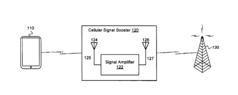
[0017] FIG. 1 illustrates an exemplary signal booster 120 in communication
with a
wireless device 110 and a base station 130. The signal booster 120 (also
referred to as a cellular signal amplifier) can improve the quality of
wireless
communication by amplifying, filtering, and/or applying other processing
.. techniques via a signal amplifier 122 to uplink signals communicated from
the
wireless device 110 to the base station 130 and/or downlink signals
communicated from the base station 130 to the wireless device 110. In other
words, the signal booster 120 can amplify or boost uplink signals and/or
downlink
signals bi-directionally. In one example, the signal booster 120 can be at a
fixed
location, such as in a home or office. Alternatively, the signal booster 120
can be
attached to a mobile object, such as a vehicle or a wireless device 110.
[0018] In one configuration, the signal booster 120 can include an integrated
device antenna 124 (e.g., an inside antenna or a coupling antenna) and an
integrated node antenna 126 (e.g., an outside antenna). The integrated node
.. antenna 126 can receive the downlink signal from the base station 130. The
downlink signal can be provided to the signal amplifier 122 via a second
coaxial
cable 127 or other type of radio frequency connection operable to communicate
radio frequency signals. The signal amplifier 122 can include one or more
cellular signal amplifiers for amplification and filtering. The downlink
signal that
has been amplified and filtered can be provided to the integrated device
antenna
124 via a first coaxial cable 125 or other type of radio frequency connection
operable to communicate radio frequency signals. The integrated device antenna
3
CA 3054219 2019-09-05
124 can wirelessly communicate the downlink signal that has been amplified and
filtered to the wireless device 110.
100191 Similarly, the integrated device antenna 124 can receive an uplink
signal
from the wireless device 110. The uplink signal can be provided to the signal
amplifier 122 via the first coaxial cable 125 or other type of radio frequency
connection operable to communicate radio frequency signals. The signal
amplifier 122 can include one or more cellular signal amplifiers for
amplification
and filtering. The uplink signal that has been amplified and filtered can be
provided to the integrated node antenna 126 via the second coaxial cable 127
or
other type of radio frequency connection operable to communicate radio
frequency signals. The integrated node antenna 126 can communicate the uplink
signal that has been amplified and filtered to a node, such as base station
130.
[00201 In one example, the signal booster 120 can send uplink signals to a
node
and/or receive downlink signals from the node. While FIG. 1 shows the node as
a base station 120, this is not intended to be limiting. The node can comprise
a
wireless wide area network (WWAN) access point (AP), a base station (BS), an
evolved Node B (eNB), a baseband unit (BBU), a remote radio head (RRH), a
remote radio equipment (RRE), a relay station (RS), a radio equipment (RE), a
remote radio unit (RRU), a central processing module (CPM), or another type of
WWAN access point.
100211 In one configuration, the signal booster 120 used to amplify the uplink
and/or a downlink signal is a handheld booster. The handheld booster can be
implemented in a sleeve of the wireless device 110. The wireless device sleeve
may be attached to the wireless device 110, but may be removed as needed. In
this configuration, the signal booster 120 can automatically power down or
cease
amplification when the wireless device 110 approaches a particular base
station.
In other words, the signal booster 120 may determine to stop performing signal
amplification when the quality of uplink and/or downlink signals is above a
defined threshold based on a location of the wireless device 110 in relation
to the
base station 130.
100221 In one example, the signal booster 120 can include a battery to provide
power to various components, such as the signal amplifier 122, the integrated
4
CA 3054219 2019-09-05
,
device antenna 124 and the integrated node antenna 126. The battery can also
power the wireless device 110 (e.g., phone or tablet). Alternatively, the
signal
booster 120 can receive power from the wireless device 110.
100231 In one configuration, the signal booster 120 can be a Federal
Communications Commission (FCC)-compatible consumer signal booster. As a
non-limiting example, the signal booster 120 can be compatible with FCC Part
20
or 47 Code of Federal Regulations (C.F.R.) Part 20.21 (March 21, 2013). In
addition, the handheld booster can operate on the frequencies used for the
provision of subscriber-based services under parts 22 (Cellular), 24
(Broadband
PCS), 27 (AWS-1, 700 MHz Lower A-E Blocks, and 700 MHz Upper C Block),
,
and 90 (Specialized Mobile Radio) of 47 C.F.R. The signal booster 120 can be
configured to automatically self-monitor its operation to ensure compliance
with
applicable noise and gain limits. The signal booster 120 can either self-
correct or
shut down automatically if the signal booster's operations violate the
regulations
defined in 47 CFR Part 20.21.
100241 In one configuration, the signal booster 120 can improve the wireless
connection between the wireless device 110 and the base station 130 (e.g.,
cell
tower) or another type of wireless wide area network (VVWAN) access point
(AP).
The signal booster 120 can boost signals for cellular standards, such as the
Third
Generation Partnership Project (3GPP) Long Term Evolution (LTE) Release 8, 9,
10, 11, 12, 13, 14, or 15 standards Or Institute of Electronics and Electrical
Engineers (IEEE) 802.16. In one configuration, the signal booster 120 can
boost
signals for 3GPP LTE Release 13Ø0 (March 2016) or other desired releases.
The signal booster 120 can boost signals from the 3GPP Technical Specification
36.101 (Release 12 Jun 2015) bands or LTE frequency bands. For example, the
signal booster 120 can boost signals from the LTE frequency bands: 2, 4, 5,
12,
13, 17, 25, and 26. In addition, the signal booster 120 can boost selected
frequency bands based on the country or region in which the signal booster is
used, including any of bands 1-70 or other bands, as disclosed in ETSI TS136
104 V13.5.0 (2016-10).
100251 The number of LTE frequency bands and the level of signal improvement
can vary based on a particular wireless device, cellular node, or location.
5
CA 3054219 2019-09-05
Additional domestic and international frequencies can also be included to
offer
increased functionality. Selected models of the signal booster 120 can be
configured to operate with selected frequency bands based on the location of
use. In another example, the signal booster 120 can automatically sense from
the wireless device 110 or base station 130 (or GPS, etc.) which frequencies
are
used, which can be a benefit for international travelers.
100261 FIG. 2 shows a wireless device 210 in communication with a signal
booster 220. The signal booster can receive signals from multiple base
stations,
such as the relatively close base station 230 and the relatively distant base
station 240.
100271 Signal boosters 220 are typically employed to enable one or more
wireless
device 210 users to communicate with a relatively distant base station 240.
The
distant base station can be used by the user's cellular signal provider.
However,
another base station 230, operated by a different cellular signal provider,
which is
operating in the same frequency band, may be located relatively close to the
signal booster 220. Downlink (DL) signals from the relatively close base
station
230 will have a much higher RSSI (lower BSCL) at the signal booster 220 than
the DL signals from the relatively far base station 240. The RSSI or BSCL
measurements of the combined DL signals from the relatively close 230 and
relatively far base stations 240 will result in significantly reduced uplink
(UL) gain
and/or noise power settings for the UL signals transmitted from the signal
booster
220 for a user of the relatively far base station 240. If the RSSI of the DL
signals
from the close base station 230 are sufficiently high, it can result in the
gain
and/or noise power of the transmitted UL signal being set sufficiently low
that the
UL signal cannot be accurately received at the relatively far base station
240.
[0028] Signal boosters, such as signal booster 220, also typically provide
amplification of UL signals over a fairly broad spectrum relative to a UE or
MS.
For example, a signal booster may provide amplification of an UL signal over
an
entire 3GPP LTE band. The broadband amplification of the band, and not just a
single signal, results in an amplification of all of the noise in the band as
well.
The amplification of the noise effectively raises the noise floor for a
receiver, such
as a base station. In order to ameliorate the effects of increasing the noise
floor,
6
CA 3054219 2019-09-05
the Federal Communication Commission (FCC) in the United States has issued
an order, in FCC Report and Order 13-21, that sets threshold levels for uplink
gain and noise levels.
[0029] In FCC Report and Order 13-21, the transmitted noise power in dBm/MHz
of consumer boosters at their uplink and downlink ports shall not exceed -103
dBm/MHz - RSSI. Where RSSI (received signal strength indication) is the
downlink composite received signal power in dBm at the booster donor port for
all
base stations in the band of operation. RSSI is expressed in negative dB units
relative to 1 mW. (2) The transmitted maximum noise power in dBm/MHz of
consumer boosters at their uplink and downlink ports shall not exceed the
following limits: (i) Fixed booster maximum noise power shall not exceed -
102.5
dBm/MHz + 20 Log10 (Frequency), where Frequency is the uplink mid-band
frequency of the supported spectrum bands in MHz. (ii) Mobile booster maximum
noise power shall not exceed - 59 dBm/MHz.
[0030] Similarly, FCC Report and Order 13-21 limits the uplink gain in dB of a
consumer booster referenced to its input and output ports such that it shall
not
exceed -34 dB - RSSI + MSCL, where RSSI is the downlink composite received
signal power in dBm at the booster donor port for all base stations in the
band of
operation. RSSI is expressed in negative dB units relative to 1 mW. MSCL
(Mobile Station Coupling Loss) is the minimum coupling loss in dB between the
wireless device and input port of the consumer booster. MSCL is to be
calculated
or measured for each band of operation and provided in compliance test
reports.
[0031] In accordance with one embodiment, a signal booster can be configured
to
channelize a DL signal received at the signal booster in a selected band.
Channelize, as used herein, can include filtering a selected band to pass
portions
of the band, or block portions of the band, to reduce the RSSI (or increase
the
BSCL) of one or more DL signals that cause an undesirable reduction in UL gain
and/or noise power of an uplink signal for a user of the signal booster. An
undesirable reduction in the UL gain and/or noise power is a reduction in the
UL
gain and/or noise power of the UL signal transmitted by the signal booster for
the
user, wherein the reduction in UL gain and/or noise power is used to protect
the
network (i.e. base stations) when no additional protection is actually
necessary.
7
CA 3054219 2019-09-05
For example, a DL signal received from a close BS may result in a relatively
high
RSSI. However, the booster may be boosting an UL signal for transmission to a
distant BS relative to the close BS. Removing, or substantially attenuating
the
signal from the close BS can result in an undesirable reduction in the UL
gain,
while not actually protecting the distant BS since a higher power UL gain can
be
used to transmit to the distant BS while staying within the parameters of the
FCC.
100321 While the FCC requirements are used as an example, they are not
intended to be limiting. Other governmental or industry standards may also
designate limits or suggestions for UL signal gain limitations for a signal
booster.
By more accurately measuring DL signals, the UL signal gain can be maximized
relative to the governmental or industry limits or suggestions.
100331 In one configuration, the repeater 220 can improve the wireless
connection
between the wireless device 210 and the base station 230 (e.g., cell tower) or
another type of wireless wide area network (WWAN) access point (AP) by
amplifying desired signals relative to a noise floor. The repeater 220 can
boost
signals for cellular standards, such as the Third Generation Partnership
Project
(3GPP) Long Term Evolution (LTE) Release 8,9, 10, 11, 12, 13, 14, 15, or 16
standards or Institute of Electronics and Electrical Engineers (IEEE) 802.16.
In
one configuration, the repeater 220 can boost signals for 3GPP LTE Release
16.2.0 (July 2019) or other desired releases.
100341 The repeater 220 can boost signals from the 3GPP Technical
Specification
(TS) 36.101 (Release 16 July 2019) bands or LTE frequency bands. For
example, the repeater 220 can boost signals from the LTE frequency bands: 2,
4,
5, 12, 13, 17, 25, and 26. In addition, the repeater 220 can boost selected
frequency bands based on the country or region in which the repeater is used,
including any of bands 1-85 or other bands, as disclosed in 3GPP TS 36.104
V16.2.0 (July 2019), and depicted in Table 1:
Table 1:
LTE Uplink (UL) operating band Downlink (DL)
operating Duplex
Operatin BS receive band Mode
g Band UE transmit BS transmit
UE receive
FuL low ¨ FLIL high FDL low ¨ FDL high
1 1920 MHz - 1980 MHz 2110 MHz - 2170 MHz
FDD
2 1850 MHz - 1910 MHz 1930 MHz - 1990 MHz
FDD
8
CA 3 054 2 1 9 2 0 1 9-0 9-05
3 1710 MHz ¨ 1785 MHz 1805 MHz ¨ 1880 MHz FDD
4 1710 MHz ¨ 1755 MHz 2110 MHz ¨ 2155 MHz FDD
824 MHz ¨ 849 MHz 869 MHz ¨ 894MHz FDD
6 ¨ ¨ FDD
(NOTE 830 MHz 840 MHz 875 MHz 885 MHz
1)
7 2500 MHz ¨ 2570 MHz 2620 MHz ¨ 2690 MHz FDD
8 880 MHz ¨ 915 MHz 925 MHz ¨ 960 MHz FDD
¨
9 1749.9 MHz 1784.9 MHz 1844.9 MHz ¨ 1879.9 FDD
MHz
1710 MHz ¨ 1770 MHz 2110 MHz ¨ 2170 MHz FDD
1427.9 MHz ¨ 1447.9 MHz 1475.9 MHz ¨ 1495.9 FDD
11
MHz
12 699 MHz ¨ 716 MHz 729 MHz ¨ 746 MHz FDD
13 777 MHz ¨ 787 MHz 746 MHz ¨ 756 MHz FDD
14 788 MHz ¨ 798 MHz 758 MHz ¨ 768 MHz FDD
Reserved Reserved FDD
16 Reserved Reserved FDD
17 704 MHz ¨ 716 MHz 734 MHz ¨ 746 MHz FDD
18 815 MHz ¨ 830 MHz 860 MHz ¨ 875 MHz FDD
19 830 MHz ¨ 845 MHz 875 MHz ¨ 890 MHz FDD
832 MHz ¨ 862 MHz 791 MHz ¨ 821 MHz FDD
1447.9 MHz ¨ 1462.9 MHz 1495.9 MHz ¨ 1510.9 FDD
21
MHz
22 3410 MHz ¨ 3490 MHz 3510 MHz ¨ 3590 MHz FDD
231 2000 MHz ¨ 2020 MHz 2180 MHz ¨ 2200 MHz FDD
24 1626.5 MHz ¨ 1660.5 MHz 1525 MHz ¨ 1559 MHz FDD
1850 MHz ¨ 1915 MHz 1930 MHz ¨ 1995 MHz FDD
26 814 MHz ¨ 849 MHz 859 MHz ¨ 894 MHz FDD
27 807 MHz ¨ 824 MHz 852 MHz ¨ 869 MHz FDD
28 703 MHz ¨ 748 MHz 758 MHz ¨ 803 MHz FDD
29 N/A 717 MHz ¨ 728 MHz FDD
(NOTE 2)
2305 MHz ¨ 2315 MHz 2350 MHz ¨ 2360 MHz FDD
31 452.5 MHz ¨ 457.5 MHz 462.5 MHz ¨ 467.5 MHz FDD
N/A 1452 MHz ¨ 1496 MHz FDD
32
(NOTE 2)
33 1900 MHz ¨ 1920 MHz 1900 MHz ¨ 1920 MHz TDD
34 2010 MHz ¨ 2025 MHz 2010 MHz ¨ 2025 MHz TDD
1850 MHz ¨ 1910 MHz 1850 MHz ¨ 1910 MHz TDD
36 1930 MHz ¨ 1990 MHz 1930 MHz ¨ 1990 MHz TDD
37 1910 MHz ¨ 1930 MHz 1910 MHz ¨ 1930 MHz TDD
38 2570 MHz ¨ 2620 MHz 2570 MHz ¨ 2620 MHz TDD
39 1880 MHz ¨ 1920 MHz 1880 MHz ¨ 1920 MHz TDD
2300 MHz ¨ 2400 MHz 2300 MHz ¨ 2400 MHz TDD
41 2496 MHz ¨ 2690 MHz 2496 MHz ¨ 2690 MHz TDD
42 3400 MHz ¨ 3600 MHz 3400 MHz ¨ 3600 MHz TDD
43 3600 MHz ¨ 3800 MHz 3600 MHz ¨ 3800 MHz TDD
44 703 MHz ¨ 803 MHz 703 MHz ¨ 803 MHz TDD
1447 MHz ¨ 1467 MHz 1447 MHz ¨ 1467 MHz TDD
46 5150 MHz ¨ 5925 MHz 5150 MHz ¨ 5925 MHz TDD
(NOTE 3,
NOTE 4)
47 5855 MHz ¨ 5925 MHz 5855 MHz ¨ 5925 MHz TDD
48 3550 MHz ¨ 3700 MHz 3550 MHz ¨ 3700 MHz TDD
49 3550 MHz ¨ 3700 MHz 3550 MHz ¨ 3700 MHz TDD
(NOTE 8)
1432 MHz - 1517 MHz 1432 MHz - 1517 MHz TDD
51 1427 MHz - 1432 MHz 1427 MHz - 1432 MHz TDD
52 3300 MHz - 3400 MHz 3300 MHz - 3400 MHz TDD
53 2483.5 MHz - 2495 MHz 2483.5 MHz - 2495 MHz TDD
65 1920 MHz ¨ 2010 MHz 2110 MHz ¨ 2200 MHz FDD
9
CA 3 054 2 1 9 2 0 1 9-0 9-05
66 1710 MHz ¨ 1780 MHz 2110 MHz ¨ 2200 MHz FDD
(NOTE 5)
67 N/A 738 MHz ¨ 758 MHz FDD
(NOTE 2)
68 698 MHz ¨ 728 MHz 753 MHz ¨ 783 MHz FDD
69 N/A 2570 MHz ¨ 2620 MHz FDD
(NOTE 2)
70 1695 MHz ¨ 1710 MHz 1995 MHz ¨ 2020 MHz FDD6
71 663 MHz ¨ 698 MHz 617 MHz ¨ 652 MHz FDD
72 451 MHz ¨ 456 MHz 461 MHz ¨ 466 MHz FDD
73 450 MHz ¨ 455 MHz 460 MHz ¨ 465 MHz FDD
74 1427 MHz ¨ 1470 MHz 1475 MHz ¨ 1518 MHz FDD
75 N/A 1432 MHz ¨ 1517 MHz FDD
(NOTE 2)
76 N/A 1427 MHz ¨ 1432 MHz FDD
(NOTE 2)
85 698 MHz 716 728 MHz ¨ 746 MHz FDD
MHz
87 410 MHz 415 420 MHz ¨ 425 MHz FDD
MHz
88 412 MHz 417 422 MHz ¨ 427 MHz FDD
MHz
NOTE 1: Band 6, 23 are not applicable.
NOTE 2: Restricted to E-UTRA operation when carrier aggregation is configured.
The
downlink operating band is paired with the uplink operating band (external) of
the carrier aggregation configuration that is supporting the configured Pcell.
NOTE 3: This band is an unlicensed band restricted to licensed-assisted
operation using
Frame Structure Type 3.
NOTE 4: Band 46 is divided into four sub-bands as in Table 5.5-1A.
NOTE 5: The range 2180 ¨2200 MHz of the DL operating band is restricted to E-
UTRA
operation when carrier aggregation is configured.
NOTE 6: The range 2010-2020 MHz of the DL operating band is restricted to E-
UTRA
operation when carrier aggregation is configured and TX-RX separation is 300
MHz. The range 2005-2020 MHz of the DL operating band is restricted to E-
UTRA operation when carrier aggregation is configured and TX-RX separation
is 295 MHz.
NOTE 7: Void
NOTE 8: This band is restricted to licensed-assisted operation using Frame
Structure
Type 3.
100351 In another configuration, the repeater 220 can boost signals from the
3GPP Technical Specification (TS) 38.104 (Release 16 July 2019) bands or 5G
frequency bands. In addition, the repeater 220 can boost selected frequency
bands based on the country or region in which the repeater is used, including
any
of bands n1 ¨ n86 in frequency range 1 (FR1), n257 ¨ n261 in frequency range 2
(FR2), or other bands, as disclosed in 3GPP TS 38.104 V16Ø0 (July 2019), and
depicted in Table 2 and Table 3:
Table 2:
NR Uplink (UL) operating band Downlink (DL) operating band
Duplex
operating BS receive / UE transmit BS transmit / UE receive
Mode
band FuL,10. ¨ FUL,high FDL,low ¨ FOL,high
n1 1920 MHz ¨ 1980 MHz 2110 MHz ¨ 2170 MHz , FDD
n2 1850 MHz ¨ 1910 MHz 1930 MHz ¨ 1990 MHz FDD
n3 1710 MHz¨ 1785 MHz 1805 MHz ¨ 1880 MHz FDD
CA 3054219 2019-09-05
n5 824 MHz -849 MHz 869 MHz -894 MHz FDD
n7 2500 MHz -2570 MHz 2620 MHz -2690 MHz FDD
n8 880 MHz - 915 MHz 925 MHz - 960 MHz FDD
n12 699 MHz- 716 MHz 729 MHz- 746 MHz FDD
n14 788 MHz -798 MHz 758 MHz -768 MHz FDD
n18 815 MHz- 830 MHz 860 MHz- 875 MHz FDD
n20 832 MHz -862 MHz 791 MHz -821 MHz FDD
n25 1850 MHz - 1915 MHz 1930 MHz - 1995 MHz FDD
n28 703 MHz -748 MHz 758 MHz -803 MHz FDD
n30 2305 MHz - 2315 MHz 2350 MHz - 2360 MHz FDD
n34 2010 MHz -2025 MHz 2010 MHz -2025 MHz TDD
n38 2570 MHz - 2620 MHz 2570 MHz -2620 MHz TDD
n39 1880 MHz -1920 MHz 1880 MHz -1920 MHz TDD
n40 2300 MHz - 2400 MHz 2300 MHz -2400 MHz TDD
n41 2496 MHz -2690 MHz 2496 MHz -2690 MHz TDD
n48 3550 MHz -3700 MHz 3550 MHz - 3700 MHz TDD
n50 1432 MHz - 1517 MHz 1432 MHz- 1517 MHz TDD
n51 1427 MHz - 1432 MHz 1427 MHz - 1432 MHz TDD
n65 1920 MHz - 2010 MHz 2110 MHz - 2200 MHz FDD
n66 1710 MHz - 1780 MHz 2110 MHz - 2200 MHz FDD
n70 1695 MHz - 1710 MHz 1995 MHz - 2020 MHz FDD
n71 663 MHz -698 MHz 617 MHz -652 MHz FDD
n74 1427 MHz- 1470 MHz 1475 MHz -1518 MHz FDD
n75 N/A 1432 MHz- 1517 MHz SDL
n76 N/A 1427 MHz - 1432 MHz SDL
n77 3300 MHz -4200 MHz 3300 MHz -4200 MHz TDD
n78 3300 MHz -3800 MHz 3300 MHz -3800 MHz TDD
n79 4400 MHz -5000 MHz 4400 MHz -5000 MHz TDD
n80 1710 MHz - 1785 MHz N/A SUL
n81 880 MHz - 915 MHz N/A SUL
n82 832 MHz -862 MHz N/A SUL
n83 703 MHz -748 MHz N/A SUL
n84 1920 MHz - 1980 MHz N/A SUL
n86 1710 MHz - 1780 MHz N/A SUL
[n90] 2496 MHz - 2690 MHz 2496 MHz - 2690 MHz TDD
Table 3:
NR Uplink (UL) and Downlink (DL) Duplex
operating operating band Mode
band BS transmit/receive
UE transmit/receive
FULlow ¨ FUL,high
FDL,low ¨ FOL,hIgh
n257 26500 MHz - 29500 MHz TDD
n258 24250 MHz - 27500 MHz TDD
n260 37000 MHz -40000 MHz TDD
n261 27500 MHz -28350 MHz TDD
10036] Channelizing the DL and UL signals in selected bands at the signal
booster can reduce interference from other DL signals from a same base station
or different base stations, thereby enabling the UL signals transmitted from
the
signal booster for a selected user to have an increased gain and increase the
range over which the selected user can communicate. In addition, channelizing
the UL signal can allow filtering that will reduce the noise power transmitted
to
base stations and allow the signal booster to meet the specification
requirements.
11
CA 3054219 2019-09-05
Filtering of the UL signal can typically occur at an equivalent location (i.e.
channel) as is filtered in the DL signal. For example, in an FDD band, such as
3GPP LTE band 5, if the bottom 15 MHz of the DL spectrum for 3GPP LTE band
is filtered to attenuate signals in those frequencies, the bottom 15 MHz of
the
5 UL spectrum for 3GPP LTE band 5 can also be similarly filtered. By
filtering the
UL signal, the noise floor can be effectively reduced, thereby enabling a base
station, such as a 3GPP LTE eNodeB, to receive the UL signal with a lower
noise
floor.
[0037] FIG. 3 provides one example of a channelization device 300 for
increasing
signal booster gain at a signal booster. The channelization device 300
comprises
a first diplexer 302 configured to be coupled to a first interface port and a
second
diplexer 304 configured to be coupled to a second interface port. In one
embodiment, the first interface port can be an outside antenna, and the second
interface port can be an inside antenna. The channelization device 300 can
include radio frequency connections to enable the channelization device 300 to
be connected to the first and/or second interface ports, or other components
such
as a signal booster.
[0038] The channelization device 300 can further comprise a controller 303.
The
channelization device 300 can further comprise a channelized filter 306. In
the
example illustrated in FIG. 3, the channelized filter 306 is comprised of a
first
channelized duplexer 308 and a second channelized duplexer 310. Switches
312, 314 can be used to create a bypass path around the channelized filter 306
to allow an uplink signal or a downlink signal to bypass the channelized
filter 306.
[0039] FIG. 4 illustrates an example of a repeater 400 for increasing signal
booster gain from a weak-signal far node in the proximity of a strong-signal
near
node. An inside antenna 402 can be coupled to a first interface port 404. The
first interface port 404 can be coupled to a first duplexer 406. An outside
antenna
408 can be coupled to a second interface port 410. The second interface port
410 can be coupled to a second duplexer 412.
100401 The first duplexer 406 can pass a signal in a first direction. The
first
direction can be an uplink direction or a downlink direction. The first
direction can
include a first low noise amplifier (LNA) 414 that can be coupled to the first
12
CA 3054219 2019-09-05
duplexer 406. The first LNA 414 can be coupled to a variable attenuator 416.
The variable attenuator 416 can be coupled to a bandpass filter 418 that can
pass a selected band of the first direction. The bandpass filter 418 can be a
third
generation partnership project (3GPP) long term evolution (LTE) frequency
division duplex (FDD) band 5 uplink bandpass filter (B5 UL BPF). The bandpass
filter 418 can be coupled to an amplifier 420.
100411 The amplifier 420 can be coupled to a splitter 422. The splitter 422
can be
a directional coupler or combiner, or can be a multiport splitter (e.g. 3-way
or 4-
way). The splitter can also be a hybrid coupler, such as a 90 degree hybrid
coupler or a 180 degree hybrid coupler. Other types of hybrid couplers may
also
be used. The splitter 422 can split the first direction into two paths: a
first
channelized switchable first-direction parallel path 424 and a first
switchable first
direction parallel path 426. The first channelized switchable first-direction
parallel
path 424 can comprise a first channelized first-direction bandpass filter 428
for a
first subset of a selected band. The selected band can be a 3GPP LTE FDD
band 5 uplink. The first subset of the selected band can be channel B of the
3GPP LTE FDD band 5 uplink. The selected band can also be one or more of a
3GPP LTE band 1 to 76 uplink and 85 uplink.
100421 The first channelized switchable first-direction parallel path 424 can
further
comprise a variable attenuator 430. The variable attenuator 430 can be coupled
between the splitter 422 and the first channelized first-direction bandpass
filter
428.
100431 The first switchable first-direction parallel path 426 can comprise: a
switchable first-direction path 432 and a second channelized switchable first-
direction parallel path 434. The switchable first-direction path 432 can
comprise
a first bandpass filter 436 for passing the selected band. The selected band
can
be 3GPP LTE FDD band 5 uplink. The second channelized switchable first-
direction parallel path 434 can comprise a second channelized first-direction
bandpass filter 438 for a second subset of the selected band. The second
subset
of the selected band can be channel A of the 3GPP LTE FDD band 5 uplink.
100441 The second channelized switchable first-direction parallel path 426 can
further comprise a variable attenuator 440. The variable attenuator 440 can be
13
CA 3054219 2019-09-05
coupled between the splitter 422 and the second channelized first-direction
bandpass filter 438 and the first bandpass filter 436.
[0045] A second splitter 442 can be coupled between the second interface port
410 and the first bandpass filter 436, the second channelized first-direction
bandpass filter 438, and the first channelized first-direction bandpass filter
428.
The second splitter 442 can be coupled to an additional bandpass filter 444
configured to pass a first-direction of the selected band. The selected band
can
be 3GPP LTE FDD band 5 uplink. The additional bandpass filter 444 can be
coupled to a radio frequency (RF) detector 446, which can be coupled to a
power
amplifier (PA) 448. The power amplifier 448 can be coupled to the second
duplexer 412, which can be coupled to the second interface port 410.
[0046] The repeater 400 can further comprise a first switch 450 for the first
switchable first-direction parallel path 426. The first switch 450 can be
coupled
between the second splitter 442 and the first bandpass filter 436 and the
second
channelized first-direction bandpass filter 438. The repeater 400 can further
comprise a second switch 452 for the first channelized switchable first-
direction
parallel path 424. The second switch 452 can be coupled between the second
splitter 442 and the first channelized first-direction bandpass filter 428.
[0047] The repeater 400 can further comprise a third switch 454. The third
switch
454 can be coupled between the first splitter 422 and the first bandpass
filter 436
and the second channelized first-direction bandpass filter 438. The repeater
400
can further comprise a fourth switch 456. The fourth switch 456 can be coupled
between the first bandpass filter 436 and the second channelized first-
direction
bandpass filter 438, and the first switch 450.
100481 The second duplexer 412 can pass a signal in a second direction. The
second direction can be an uplink direction or a downlink direction. The
second
direction can include a low noise amplifier 458 that can be coupled to a
bandpass
filter 460. The bandpass filter 460 can pass a second direction of a selected
band. The selected band can be a 3GPP LTE band 5 downlink. The selected
band can also be one or more of a 3GPP LTE band 1 to 76 downlink and 85
downlink. The bandpass filter 460 can be coupled to an amplifier 462 which can
be coupled to a variable attenuator 464 and an additional bandpass filter 466.
14
CA 3054219 2019-09-05
The additional bandpass filter 466 can pass a second direction of the selected
band and can be coupled to a first second-direction splitter 468.
100491 The first second-direction splitter 468 can be a directional coupler or
combiner, and can be a multiport splitter (e.g. 3-way or 4-way). The splitter
468
can split the second direction into two paths: a first channelized switchable
second-direction parallel path 470 and a first switchable second-direction
parallel
path 472. The first channelized switchable second-direction parallel path 470
can
be coupled to the first second-direction splitter 468, and the first
channelized
switchable second-direction parallel path 470 can comprise a first channelized
second-direction filter 474 for a first subset of the selected band. The
selected
band can be a 3GPP LTE FDD band 5 downlink. The first subset of the selected
band can be channel B of the 3GPP LTE FDD band 5 downlink.
100501 The first channelized switchable second-direction parallel path 470 can
further comprise a variable attenuator 476. The variable attenuator 476 can be
coupled between the first second-direction splitter 468 and the first
channelized
second-direction bandpass filter 474.
100511 The first switchable second-direction parallel path 472 can comprise: a
switchable second-direction path 478 and a second channelized switchable
second-direction parallel path 480. The switchable second-direction path 478
can comprise a second bandpass filter 482 for passing the selected band. The
selected band can be 3GPP LTE FDD band 5 downlink. The second channelized
switchable second-direction parallel path 480 can comprise a second
channelized second-direction bandpass filter 484 for a second subset of the
selected band. The second subset of the selected band can be channel A of the
3GPP LTE FDD band 5 downlink.
100521 The first switchable second-direction parallel path 472 can further
comprise a variable attenuator 477. The variable attenuator 477 can be coupled
between the first second-direction splitter 468, the second bandpass filter
482,
and the second channelized second-direction bandpass filter 484.
10053] A second second-direction splitter 486 can be coupled between the first
interface port 404 and the first channelized second-direction bandpass filter
474,
the second bandpass filter 482, and the second channelized second-direction
CA 3054219 2019-09-05
bandpass filter 484. The second second-direction splitter 486 can be coupled
to
an additional bandpass filter 488 configured to pass a second-direction of the
selected band. The selected band can be 3GPP LTE FDD band 5 downlink. The
additional bandpass filter 488 can be coupled to an RF detector 490, which can
.. be coupled to a power amplifier 492. The power amplifier 492 can be coupled
to
the first duplexer 406, which can be coupled to the first interface port 404.
100541 The repeater 400 can further comprise a first second-direction switch
494
for the first switchable second-direction parallel path 472. The first second-
direction switch 494 can be coupled between the second second-direction
splitter
.. 486 and the second bandpass filter 482 and the second channelized second-
direction bandpass filter 484. The repeater 400 can further comprise a second
second-direction switch 496 for the first channelized switchable second-
direction
parallel path 470. The second second-direction switch 496 can be coupled
between the second second-direction splitter 486 and the first channelized
.. second-direction bandpass filter 474.
100551 The repeater 400 can further comprise a third second-direction switch
498.
The third second-direction switch 498 can be coupled between the first second-
direction splitter 468 and the second bandpass filter 482 and the second
channelized second-direction bandpass filter 484. The repeater 400 can further
.. comprise a fourth second-direction switch 499. The fourth second-direction
switch 499 can be coupled between the second bandpass filter 482 and the
second channelized second-direction bandpass filter 484, and the first second-
direction switch 494.
100561 The repeater 400 can operate in wideband mode or parallel channelized
.. mode. Wideband mode can be used by disabling the Channel B path (Le. the
path with the B5 UL ChB BPF and the B5 DL ChB BPF) and switching into the
wideband BPF (i.e. B5 UL BPF and B5 DL BPF). The received signal strength
indicator (RSSI) of channel A and channel B can be identified separately by
disabling the undesired channel during signal detection. Alternatively,
separate
.. detectors can be used on each signal path. The switches in the repeater 400
can
be one method of maintaining impedance matching to the splitter if any of
Enable
1 through 4 are disabled.
16
CA 3054219 2019-09-05
[00571 FIG. 5 illustrates an example of a repeater 500 for increasing signal
booster gain from a weak-signal far node in the proximity of a strong-signal
near
node. An inside antenna 502 can be coupled to a first interface port 504. The
first interface port 504 can be coupled to a first duplexer 506. An outside
antenna
508 can be coupled to a second interface port 510. The second interface port
510 can be coupled to a second duplexer 512.
100581 The first duplexer 506 can pass a signal in a first direction. The
first
direction can be an uplink direction or a downlink direction. The first
direction can
include a first low noise amplifier (LNA) 514a that can be coupled to the
first
duplexer 506. The first LNA 514a can be coupled to a variable attenuator 516a.
The variable attenuator 516a can be coupled to switch 518a. The switch 518a
can direct a signal onto a switchable first-direction parallel path comprising
a
switchable first-direction path 520a and a switchable first-direction path
522a.
The switchable first-direction path 520a can comprise a bandpass filter 524a
for
passing a first selected first-direction band. The bandpass filter 524a can be
a
third generation partnership project (3GPP) long term evolution (LTE)
frequency
division duplex (FDD) band 5 uplink bandpass filter (B5 UL). The switchable
first-
direction path 522a can comprise a bandpass filter 526a for passing a second
selected first-direction band. The bandpass filter 526a can be a 3GPP LTE FDD
band 26 uplink bandpass filter (B26 UL).The bandpass filter 524a and the
bandpass filter 526a can be coupled to a switch 528a. The switch 528a can be
coupled to an amplifier 530a. The amplifier 530a can be coupled to a variable
attenuator 532a.
100591 The variable attenuator 532a can be coupled to a switch 534a. The
switch
534a can be coupled to another switch 536a and a splitter 538a. The switch
536a can direct a signal onto a switchable first-direction parallel path
comprising
a switchable first-direction path 540a and a switchable first-direction path
542a.
The switchable first-direction path 540a can comprise a bandpass filter 544a
for
passing a first selected first-direction band. The bandpass filter 544a can be
a
.. 3GPP LTE FDD band 5 uplink bandpass filter (B5 UL). The switchable first-
direction path 542a can comprise a bandpass filter 546a for passing a second
selected first-direction band. The bandpass filter 546a can be a 3GPP LTE FDD
17
CA 3054219 2019-09-05
band 26 uplink bandpass filter (B26 UL). The bandpass filter 544a and the
bandpass filter 546a can be coupled to a switch 548a. The switch 548a can be
coupled to another switch 550a.
100601 The splitter 538a can be a directional coupler or combiner, and can be
a
multiport splitter (e.g. 3-way or 4-way). The splitter 538a can split the
first
direction into two paths: a channelized switchable first-direction parallel
path
552a and a switchable first-direction parallel path 554a. The channelized
switchable first-direction parallel path 552a can comprise a channelized first-
direction bandpass filter 556a for a first subset of a first selected first-
direction
band. The bandpass filter 556a can be a 3GPP LTE FDD band 5 channel B
uplink bandpass filter (5B UL). The selected first-direction band can be a
3GPP
LTE FDD band 5 uplink. The first subset of the selected first-direction band
can
be channel B of the 3GPP LTE FDD band 5 uplink. The bandpass filter 556a can
be coupled to a power detector 558a which can be coupled to a variable
attenuator 560a. The variable attenuator 560a can be coupled to a combiner
562a. The combiner 562a can be coupled to the switch 550a.
100611 The switchable first-direction parallel path 554a can comprise a switch
555a and can further comprise a channelized switchable first-direction
parallel
path 564a and a switchable first-direction path 566a. The channelized
switchable
first-direction parallel path 564a can comprise a channelized first-direction
bandpass filter 568a for a second subset of a first selected first-direction
band.
The bandpass filter 568a can be a 3GPP LTE FDD band 5 channel A uplink
bandpass filter (5A UL). The first selected first-direction band can be a 3GPP
LTE FDD band 5 uplink. The second subset of the first selected first-direction
band can be channel A of the 3GPP LTE FDD band 5 uplink. The switchable
first-direction path 566a can comprise a filter 570a for passing the second
subset
of the first selected first-direction band and a first subset of a second
selected
first-direction band. The filter 570a can be a 3GPP LTE FDD band 5A+26 uplink
bandpass filter (5A+26 UL). The first selected first-direction band can be a
3GPP
LTE FDD band 5 uplink. The second subset of the first selected first-direction
band can be channel A of the 3GPP LTE FDD band 5 uplink. The second
selected first-direction band can be a 3GPP LTE FDD band 26 uplink. The first
18
CA 3054219 2019-09-05
subset of the second selected first-direction band can be a channel delta of
the
3GPP LTE FDD band 26 uplink. 3GPP LTE FDD band 5 uplink can include the
frequencies 824 megahertz (MHz) through 849 MHz. 3GPP LTE FDD band 5
channel A uplink can include the frequencies 824 MHz through 835 MHz. 3GPP
LTE FDD band 5 channel B uplink can include the frequencies 835 MHz through
845 MHz. 3GPP LTE FDD band 26 uplink can include the frequencies 814 MHz
through 849 MHz. Channel delta of the 3GPP LTE FDD band 26 uplink can
include the frequencies 814 MHz through 824 MHz.
100621 The bandpass filter 568a and the filter 570a can be coupled to a switch
572a. The switch 572a can be coupled to a power detector 574a which can be
coupled to a variable attenuator 576a. The variable attenuator 576a can be
coupled to the combiner 562a. The combiner 562a can be coupled to the switch
550a.
[00631 The switch 550a can be coupled to an amplifier 578a which can be
coupled to a variable attenuator 580a. The variable attenuator 580a can be
coupled to a first-direction bandpass filter 582a. The first-direction
bandpass filter
582a can be a 3GPP LTE FDD band 26 uplink bandpass filter (B26 UL). The
first-direction bandpass filter 582a can be coupled to a power detector 584a.
The
power detector 584a can be coupled to a power amplifier 586a. The power
amplifier 586a can be coupled to the second duplexer 512.
100641 The second duplexer 512 can pass a signal in a second direction. The
second direction can be an uplink direction or a downlink direction. The
second
direction can include a low noise amplifier (LNA) 514b that can be coupled to
the
second duplexer 512. The LNA 514b can be coupled to a variable attenuator
516b. The variable attenuator 516b can be coupled to switch 518b. The switch
518b can direct a signal onto a switchable second-direction parallel path
comprising a switchable second-direction path 520b and a switchable second-
direction path 522b. The switchable second-direction path 520b can comprise a
bandpass filter 524b for passing a first selected second-direction band. The
bandpass filter 524b can be a third generation partnership project (3GPP) long
term evolution (LTE) frequency division duplex (FDD) band 5 downlink bandpass
filter (B5 DL). The switchable second-direction path 522b can comprise a
19
CA 3054219 2019-09-05
bandpass filter 526b for passing a second selected second-direction band. The
bandpass filter 526b can be a 3GPP LTE FDD band 26 downlink bandpass filter
(B26 DL).The bandpass filter 524b and the bandpass filter 526b can be coupled
to a switch 528b. The switch 528b can be coupled to an amplifier 530b. The
amplifier 530b can be coupled to a variable attenuator 532b.
100651 The variable attenuator 532b can be coupled to a switch 534b. The
switch
534b can be coupled to another switch 536b and a splitter 538b. The switch
536b can direct a signal onto a switchable second-direction parallel path
comprising a switchable second-direction path 540b and a switchable second-
direction path 542b. The switchable second-direction path 540b can comprise a
bandpass filter 544b for passing a first selected second-direction band. The
bandpass filter 544b can be a 3GPP LTE FDD band 5 downlink bandpass filter
(B5 DL). The switchable second-direction path 542b can comprise a bandpass
filter 546b for passing a second selected second-direction band. The bandpass
filter 546b can be a 3GPP LTE FDD band 26 downlink bandpass filter (B26 DL).
The bandpass filter 544b and the bandpass filter 546b can be coupled to a
switch
548b. The switch 548b can be coupled to another switch 550b.
100661 The splitter 538b can be a directional coupler or combiner, and can be
a
multiport splitter (e.g. 3-way or 4-way). The splitter 538b can split the
second
direction into two paths: a channelized switchable second-direction parallel
path
552b and a switchable second-direction parallel path 554b. The channelized
switchable second-direction parallel path 552b can comprise a channelized
second-direction bandpass filter 556b for a first subset of a first selected
second-
direction band. The bandpass filter 556b can be a 3GPP LTE FDD band 5
channel B downlink bandpass filter (5B DL). The selected second-direction band
can be a 3GPP LTE FDD band 5 downlink. The first subset of the selected
second-direction band can be channel B of the 3GPP LTE FDD band 5 downlink.
The bandpass filter 556b can be coupled to a power detector 558b which can be
coupled to a variable attenuator 560b. The variable attenuator 560b can be
coupled to a combiner 562b. The combiner 562b can be coupled to the switch
550b.
[0067] The switchable second-direction parallel path 554b can comprise a
switch
CA 3054219 2019-09-05
555b and can further comprise a channelized switchable second-direction
parallel
path 564b and a switchable second-direction path 566b. The channelized
switchable second-direction parallel path 564b can comprise a channelized
second-direction bandpass filter 568b for a second subset of a first selected
second-direction band. The bandpass filter 568b can be a 3GPP LTE FDD band
5 channel A downlink bandpass filter (5A DL). The first selected second-
direction
band can be a 3GPP LTE FDD band 5 downlink. The second subset of the first
selected second-direction band can be channel A of the 3GPP LTE FDD band 5
downlink. The switchable second-direction path 566b can comprise a filter 570b
for passing the second subset of the first selected second-direction band and
a
first subset of a second selected second-direction band. The filter 570b can
be a
3GPP LTE FDD band 5A+26 downlink bandpass filter (5A+26 DL). The first
selected second-direction band can be a 3GPP LTE FDD band 5 downlink. The
second subset of the first selected second-direction band can be channel A of
the
3GPP LTE FDD band 5 downlink. The second selected second-direction band
can be a 3GPP LTE FDD band 26 downlink. The first subset of the second
selected second-direction band can be a channel delta of the 3GPP LTE FDD
band 26 downlink. 3GPP LTE FDD band 5 downlink can include the frequencies
869 MHz through 894 MHz. 3GPP LTE FDD band 5 channel A downlink can
include the frequencies 869 MHz through 880 MHz. 3GPP LTE FDD band 5
channel B downlink can include the frequencies 880 MHz through 890 MHz.
3GPP LTE FDD band 26 downlink can include the frequencies 859 MHz through
894 MHz. Channel delta of the 3GPP LTE FDD band 26 downlink can include
the frequencies 859 MHz through 869 MHz.
100681 The bandpass filter 568b and the filter 570b can be coupled to a switch
572b. The switch 572b can be coupled to a power detector 574b which can be
coupled to a variable attenuator 576b. The variable attenuator 576b can be
coupled to the combiner 562b. The combiner 562b can be coupled to the switch
550b.
100691 The switch 550b can be coupled to an amplifier 578b which can be
coupled to a variable attenuator 580b. The variable attenuator 580b can be
coupled to a second-direction bandpass filter 582b. The second-direction
21
CA 3054219 2019-09-05
bandpass filter 582b can be a 3GPP LTE FDD band 26 downlink bandpass filter
(B26 DL). The second-direction bandpass filter 582b can be coupled to a power
detector 584b. The power detector 584b can be coupled to a power amplifier
586b. The power amplifier 586b can be coupled to the first duplexer 506.
100701 The repeater 500 can be configured for B26 and full B5 mode (e.g., in
which UL filter banks A and B can operate) or parallel channelized mode (e.g.,
in
which UL filter bank C can operate). Separate detectors can be used to
identify
the RSSI of band 5 channel A and band 5 channel B. The RSSI of band 26 and
band 5 can be identified separately by switching to the desired filters filter
banks
A and B.
100711 FIG. 6 illustrates an example of a repeater 600 for increasing signal
booster gain from a weak-signal far node in the proximity of a strong-signal
near
node. An outside antenna 602 can be coupled to a first interface port 604. The
first interface port 604 can be coupled to a first multiplexer 606. An inside
antenna 608 can be coupled to a second interface port 610. The second
interface port 610 can be coupled to a second multiplexer 612.
100721 The first multiplexer 606 can pass a signal in a first direction. The
first
direction can be a downlink direction or an uplink direction. The first
direction can
include a first low noise amplifier 614 that can be coupled to the first
multiplexer
606. The first low noise amplifier 614 can be coupled to a dual bandpass
filter
616 that can pass a selected dual-band of the first direction. The dual
bandpass
filter 616 can be coupled to an amplifier 618. The amplifier 618 can be
coupled to
a variable attenuator 620. The variable attenuator 620 can be coupled to an
additional dual bandpass filter 622.
100731 The additional dual bandpass filter 622 can be coupled to a splitter
624.
The splitter 624 can be a directional coupler or combiner, and can be a
multiport
splitter (e.g. 3-way or 4-way). The splitter 624 can split the first direction
into two
paths: a first band-specific switchable first-direction parallel path 626 and
a first
switchable first-direction parallel path 628. The first band-specific
switchable first-
direction parallel path 626 can comprise a first first-direction bandpass
filter 630
for a first band of the selected dual-band. The selected dual-band can be a
third
generation partnership project (3GPP) long term evolution (LTE) frequency
22
CA 3054219 2019-09-05
division duplex (FDD) band 12 and 13 downlink. The first band of the selected
dual-band can be 3GPP LTE FDD band 12 downlink or 13 downlink.
100741 The first band-specific switchable first-direction parallel path 626
can
further comprise a variable attenuator 632. The variable attenuator 632 can be
coupled between the splitter 624 and the first first-direction bandpass filter
630.
100751 The first switchable first direction parallel path 628 can comprise: a
dual-
band switchable first-direction path 634 and a second band-specific switchable
first-direction parallel path 636. The dual-band switchable first-direction
path 634
can comprise a second first-direction bandpass filter 638 for passing the
selected
dual-band. The selected dual-band can be 3GPP LTE FDD band 12 downlink
and 13 downlink. The second band-specific switchable first-direction parallel
path
636 can comprise a third first-direction bandpass filter 640 for a second band
of
the selected dual-band. The second band of the selected dual-band can be
3GPP LTE FDD band 12 downlink or 13 downlink.
100761 The first switchable first direction parallel path 628 can further
comprise a
variable attenuator 642. The variable attenuator 642 can be coupled between
the
splitter 624 and the second first-direction bandpass filter 638 and the third
first-
direction bandpass filter 640.
[00771 A second splitter 644 can be coupled between the second interface port
610 and the first first-direction bandpass filter 630, the second first-
direction
bandpass filter 638, and the third first-direction bandpass filter 640. The
second
splitter 644 can be coupled to an additional dual bandpass filter 646
configured to
pass a selected dual-band. The selected dual-band can be a 3GPP LTE FDD
band 12 and 13 downlink. The additional dual bandpass filter 646 can be
coupled to a radio frequency (RE) detector 648, which can be coupled to a
power
amplifier 650. The power amplifier 650 can be coupled to the second
multiplexer
612, which can be coupled to the second interface port 610.
100781 The repeater 600 can further comprise a first switch 652 for the first
switchable first-direction parallel path 628. The first switch 652 can be
coupled
between the second splitter 644 and the second first-direction bandpass filter
638
and the third first-direction bandpass filter 640. The repeater 600 can
further
comprise a second switch 654 for the first band-specific switchable first-
direction
23
CA 3054219 2019-09-05
parallel path 626. The second switch 654 can be coupled between the second
splitter 644 and the first first-direction bandpass filter 630.
[0079] The repeater 600 can further comprise a third switch 656. The third
switch
656 can be coupled between the first splitter 624 and the second first-
direction
bandpass filter 638 and the third first-direction bandpass filter 640. The
repeater
600 can further comprise a fourth switch 658. The fourth switch 658 can be
coupled between the second first-direction bandpass filter 638 and the third
first-
direction bandpass filter 640, and the first switch 652.
[0080] The second multiplexer 612 can pass a signal in a second direction. The
second direction can be an uplink direction or a downlink direction. The
second
direction can include a low noise amplifier 660 that can be coupled to a
variable
attenuator 661. The variable attenuator 661 can be coupled to a first second-
direction bandpass filter 662. The first second-direction bandpass filter 662
can
pass a first selected band of a second-direction signal. The first selected
band
can be a 3GPP LTE FDD band 12 uplink or 13 uplink. The selected band can
also be one or more of a 3GPP LTE FDD band 1 to 76 uplink and 85 uplink. The
first second-direction bandpass filter 662 can be coupled to an amplifier 663
which can be coupled to a variable attenuator 664. The variable attenuator 664
can be coupled to a first second-direction switch 665.
100811 The first second-direction switch 665 can direct the second direction
into
two paths: a first channelized switchable second-direction parallel path 666
and a
first switchable second-direction parallel path 667. The first channelized
switchable second-direction parallel path 666 can be coupled to the first
second-
direction switch 665, and the first channelized switchable second-direction
parallel path 666 can comprise a first channelized second-direction filter 668
for a
first subset of the selected band. The selected band can be a 3GPP LTE FDD
band 12 uplink or 13 uplink. The first switchable second-direction parallel
path
667 coupled to the first second-direction switch 665 can comprise a second
second-direction bandpass filter 669 for the first selected band. The selected
band can be a 3GPP LTE FDD band 12 uplink or 13 uplink.
[0082] The repeater 600 can further comprise an additional second-direction
switch 670. The additional second-direction switch 670 can be coupled between
24
CA 3054219 2019-09-05
the first channelized second-direction filter 668 and the second second-
direction
bandpass filter 669 and an additional amplifier 671.
100831 The additional amplifier 671 can be coupled to an additional bandpass
filter 672 for the first selected band. The first selected band can be a 3GPP
LTE
FDD band 12 uplink or 13 uplink. The additional bandpass filter 672 can be
coupled to a radio frequency (RF) detector 673, which can be coupled to a
power
amplifier 674. The power amplifier 674 can be coupled to the first multiplexer
606, which can be coupled to the first interface port 604.
100841 The second multiplexer 612 can pass an additional signal in a second
direction. The second direction can be an uplink direction or a downlink
direction.
The second direction can include a low noise amplifier 680 that can be coupled
to
a variable attenuator 681. The variable attenuator 681 can be coupled to a
third
second-direction bandpass filter 682. The third second-direction bandpass
filter
682 can pass a second selected band of a second-direction signal. The second
selected band can be a 3GPP LTE FDD band 12 uplink or 13 uplink. The
selected band can also be one or more of a 3GPP LTE FDD band 1 to 76 uplink
and 85 uplink. The third second-direction bandpass filter 682 can be coupled
to
an additional amplifier 683 which can be coupled to a variable attenuator 684.
The variable attenuator 684 can be coupled to a second second-direction switch
685.
100851 The second second-direction switch 685 can direct the second direction
into two paths: a second channelized switchable second-direction parallel path
686 and a second switchable second-direction parallel path 687. The second
channelized switchable second-direction parallel path 686 can be coupled to
the
second second-direction switch 685, and the second channelized switchable
second-direction parallel path 686 can comprise a second channelized second-
direction filter 688 for a second subset of the second selected band. The
second
selected band can be a 3GPP LTE FDD band 12 uplink or 13 uplink. The second
switchable second-direction parallel path 687 can be coupled to the second
second-direction switch 685 that can comprise a fourth second-direction
bandpass filter 689 for the second selected band. The selected band can be a
3GPP LTE FDD band 12 uplink or 13 uplink.
CA 3054219 2019-09-05
[0086] The repeater 600 can further comprise an additional second-direction
switch 690. The additional second-direction switch 690 can be coupled between
the second channelized second-direction filter 688 and the fourth second-
direction bandpass filter 689 and an additional amplifier 691.
[0087] The additional amplifier 691 can be coupled to an additional bandpass
filter 692 for the second selected band. The second selected band can be a
3GPP LTE FDD band 12 uplink or 13 uplink. The additional bandpass filter 692
can be coupled to a radio frequency (RF) detector 693, which can be coupled to
a power amplifier 694. The power amplifier 694 can be coupled to the first
multiplexer 606, which can be coupled to the first interface port 604.
[0088] The repeater 600 can operate in wideband mode or parallel channelized
mode (in which band 12 and band 13 can be adjusted separately). For wideband
mode, the filter can be switched to the wideband BPF for UL and DL (i.e. B12
UL
BPF, B13 UL BPF, and B12/13 DL BPF), and the downlink channelized filter can
be disabled (i.e. B13 DL Chan BPF). The RSSI of band 12 and band 13 can be
separately identified by disabling the undesired channel during signal
detection.
Alternatively, separate detectors can be used on each signal path. The
switches
in the repeater 600 can be one method of maintaining impedance matching to the
splitter if any of Enable 1 through 4 are disabled. Another method includes
operating B12/13 as full uplink and having the downlink switch between B12 or
B13 BPFs, which can keep the passed band full but block the other band.
[0089] While various embodiments described herein, and illustrated in FIGS. 1-
6,
have been described with respect to a cellular signal amplifier with an
outside
antenna and an inside antenna, this is not intended to be limiting. A repeater
for
increasing signal booster gain from a weak-signal far node in the proximity of
a
strong-signal near node can also be accomplished using a handheld booster, as
illustrated in FIG. 7. The handheld booster can include an integrated device
antenna and the integrated node antenna that are typically used in place of
the
indoor antenna and outdoor antenna, respectively.
Another example provides an apparatus 800 of a repeater for increasing signal
booster gain from a weak-signal far node in the proximity of a strong-signal
near
node, as shown in the flow chart in FIG. 8. The apparatus comprises a first
26
CA 3054219 2019-09-05
interface port, as shown in block 810. The apparatus further comprises a
second
interface port, as shown in block 820. The apparatus further comprises a first
splitter coupled to the first interface port, as shown in block 830. The
apparatus
further comprises a first channelized switchable first-direction parallel path
coupled to the first splitter comprising a first channelized first-direction
bandpass
filter for a first subset of a selected first-direction band, as shown in
block 840.
The apparatus further comprises: a first switchable first-direction parallel
path
coupled to the first splitter comprising:: a switchable first-direction path
comprising a first bandpass filter for passing the selected first-direction
band; and
a second channelized switchable first-direction parallel path comprising a
second
channelized first-direction bandpass filter for a second subset of the
selected
first-direction band, as shown in block 850.
[0090] Another example provides an apparatus 900 of a repeater for increasing
signal booster gain from a weak-signal far node in the proximity of a strong-
signal
near node, as shown in the flow chart in FIG. 9. The apparatus comprises a
first
interface port, as shown in block 910. The apparatus further comprises a
second
interface port, as shown in block 920. The apparatus further comprises a first-
direction dual-bandpass filter, coupled to the first interface port,
comprising a first-
direction filter configured to filter a selected dual-band of a first-
direction signal,
as shown in block 930. The apparatus further comprises a first splitter
coupled to
the first-direction dual-bandpass filter, as shown in block 940. The apparatus
further comprises a first band-specific switchable first-direction parallel
path
coupled to the first splitter comprising a first first-direction bandpass
filter for a
first band of the selected dual-band, as shown in block 950. The apparatus
further comprises: a first switchable first-direction parallel path coupled to
the first
splitter comprising: a dual-band switchable first-direction path comprising a
second first-direction bandpass filter for the selected dual-band; and a
second
band-specific switchable first-direction parallel path comprising a third
first-
direction bandpass filter for a second band of the selected dual-band, as
shown
in block 960.
10091] Another example provides an apparatus 1000 of a repeater for increasing
signal booster gain from a weak-signal far node in the proximity of a strong-
signal
27
CA 3054219 2019-09-05
near node, as shown in the flow chart in FIG. 10. The apparatus comprises a
first
interface port, as shown in block 1010. The apparatus further comprises a
second interface port, as shown in block 1020. The apparatus further comprises
a first splitter coupled to the first interface port, as shown in block 1030.
The
apparatus further comprises a first channelized switchable first-direction
parallel
path coupled to the first splitter comprising a first channelized first-
direction
bandpass filter for a first subset of a first selected first-direction band,
as shown in
block 1040. The apparatus further comprises a first switchable first-direction
parallel path coupled to the first splitter comprising: a second channelized
switchable first-direction parallel path comprising a second channelized first-
direction bandpass filter for a second subset of the first selected first-
direction
band; and a first switchable first-direction path comprising a first filter
for passing
the second subset of the first selected first-direction band and a first
subset of a
second selected first-direction band, as shown in block 1050.
Examples
[0092] The following examples pertain to specific technology embodiments and
point out specific features, elements, or actions that can be used or
otherwise
combined in achieving such embodiments.
[0093] Example 1 includes a repeater for increasing signal booster gain from a
weak-signal far node in the proximity of a strong-signal near node, the
repeater
comprising: a first interface port; a second interface port; a first splitter
coupled to
the first interface port; a first channelized switchable first-direction
parallel path
coupled to the first splitter comprising a first channelized first-direction
bandpass
filter for a first subset of a selected first-direction band; and a first
switchable first-
direction parallel path coupled to the first splitter comprising: a switchable
first-
direction path comprising a first bandpass filter for passing the selected
first-
direction band; and a second channelized switchable first-direction parallel
path
comprising a second channelized first-direction bandpass filter for a second
subset of the selected first-direction band.
[0094] Example 2 includes the repeater of Example 1, the repeater further
comprising: a second splitter coupled between the second interface port and
the
first bandpass filter, the second channelized first-direction bandpass filter,
and the
28
CA 3054219 2019-09-05
first channelized first-direction bandpass filter.
[0095] Example 3 includes the repeater of Example 2, the repeater further
comprising: a first switch for the first switchable first-direction parallel
path,
wherein the first switch is coupled between: the second splitter; and the
first
bandpass filter and the second channelized first-direction bandpass filter;
and a
second switch for the first channelized switchable first-direction parallel
path,
wherein the second switch is coupled between: the second splitter; and the
first
channelized first-direction bandpass filter.
[0096] Example 4 includes the repeater of Example 3, the repeater further
comprising: a third switch coupled between: the first splitter; and the first
bandpass filter and the second channelized first-direction bandpass filter; a
fourth
switch coupled between: the first bandpass filter and the second channelized
first-direction bandpass filter; and the first switch.
[0097] Example 5 includes the repeater of Example 1, the repeater further
comprising: a first second-direction splitter coupled to the second interface
port; a
first channelized switchable second-direction parallel path coupled to the
first
second-direction splitter comprising a first channelized second-direction
bandpass filter for a first subset of the selected second-direction band; and
a first
switchable second-direction parallel path coupled to the first second-
direction
splitter comprising: a switchable second-direction path comprising a second
bandpass filter for passing the selected second-direction band; and a second
channelized switchable second-direction parallel path comprising a second
channelized second-direction bandpass filter for a second subset of the
selected
second-direction band.
100981 Example 6 includes the repeater of Example 5, the repeater further
comprising: a second second-direction splitter coupled between the first
interface
port and the first channelized second-direction bandpass filter, second
bandpass
filter, and the second channelized second-direction bandpass filter.
[0099] Example 7 includes the repeater of Example 6, the repeater further
comprising: a first second-direction switch for the first switchable second-
direction
parallel path, wherein the first second-direction switch is coupled between:
the
second second-direction splitter; and the second bandpass filter and the
second
29
CA 3054219 2019-09-05
channelized second-direction bandpass filter; and a second second-direction
switch for the first channelized switchable second-direction parallel path,
wherein
the second second-direction switch is coupled between: the second second-
direction splitter; and the first channelized second-direction bandpass
filter.
[00100] Example 8 includes the repeater of Example 7, the repeater further
comprising: a third second-direction switch coupled between: the first second-
direction splitter; and the second bandpass filter and the second channelized
second-direction bandpass filter; a fourth second-direction switch coupled
between: the second bandpass filter and the second channelized second-
direction bandpass filter; and the first second-direction switch.
[00101] Example 9 includes the repeater of Example 1, the repeater further
comprising: a first duplexer configured to be coupled to the first interface
port;
and a second duplexer configured to be coupled to the second interface port.
[00102] Example 10 includes the repeater of Example 9, the repeater further
comprising: a first-direction bandpass filter, coupled to the first duplexer,
comprising a first-direction filter configured to filter the selected first-
direction
band.
[00103] Example 11 includes the repeater of Example 1, wherein the selected
first-direction band is a third generation partnership project (3GPP) long
term
evolution (LTE) frequency division duplex band 5 uplink.
[00104] Example 12 includes the repeater of Example 5, wherein the selected
second-direction band is a third generation partnership project (3GPP) long
term
evolution (LTE) frequency division duplex band 5 downlink.
[00105] Example 13 includes the repeater of Example 1, wherein the selected
first-direction band is selected as one or more of: a third generation
partnership
project (3GPP) long term evolution (LTE) band 1 to 76 uplink and 85 uplink.
[00106] Example 14 includes the repeater of Example 5, wherein the selected
second-direction band is selected as one or more of: a third generation
partnership project (3GPP) long term evolution (LTE) band 1 to 76 downlink and
85 downlink.
1001071 Example 15 includes the repeater of Example 5, wherein the first-
CA 3054219 2019-09-05
direction is an uplink direction and the second-direction is a downlink
direction.
[00108] Example 16 includes A repeater for increasing signal booster gain from
a weak-signal far node in the proximity of a strong-signal near node, the
repeater
comprising: a first interface port; a second interface port; a first-direction
dual-
bandpass filter, coupled to the first interface port, comprising a first-
direction filter
configured to filter a selected dual-band of a first-direction signal; a first
splitter
coupled to the first-direction dual-bandpass filter; a first band-specific
switchable
first-direction parallel path coupled to the first splitter comprising a first
first-
direction bandpass filter for a first band of the selected dual-band; and a
first
switchable first-direction parallel path coupled to the first splitter
comprising: a
dual-band switchable first-direction path comprising a second first-direction
bandpass filter for the selected dual-band; and a second band-specific
switchable
first-direction parallel path comprising a third first-direction bandpass
filter for a
second band of the selected dual-band.
[00109] Example 17 includes the repeater of Example 16, the repeater further
comprising: a second splitter coupled between the second interface port and
the
first first-direction bandpass filter, second first-direction bandpass filter,
and the
third first-direction bandpass filter.
[00110] Example 18 includes the repeater of Example 17, the repeater further
comprising: a first switch for the first switchable first-direction parallel
path,
wherein the first switch is coupled between: the second splitter; and the
second
first-direction bandpass filter and the third first-direction bandpass filter;
and a
second switch for the first band-specific switchable first-direction parallel
path,
wherein the second switch is coupled between: the second splitter; and the
first
first-direction bandpass filter.
[00111] Example 19 includes the repeater of Example 18, the repeater further
comprising: a third switch coupled between: the first splitter; and the second
first-
direction bandpass filter and the third first-direction bandpass filter; and a
fourth
switch coupled between: the second first-direction bandpass filter and the
third
first-direction bandpass filter; and the first switch.
[00112] Example 20 includes the repeater of Example 16, the repeater further
comprising: a first second-direction bandpass filter, coupled to the second
31
CA 3054219 2019-09-05
interface port, comprising a second-direction filter configured to filter a
first
selected band of a second-direction signal; a first second-direction switch
coupled to the first second-direction bandpass filter; a first channelized
switchable second-direction parallel path coupled to the first second-
direction
switch comprising a first second-direction channelized bandpass filter for a
channel of the first selected band; and a first switchable second-direction
parallel
path coupled to the first second-direction switch comprising a first second-
direction path comprising a second second-direction bandpass filter for the
first
selected band.
1001131 Example 21 includes the repeater of Example 20, the repeater further
comprising: a third second-direction bandpass filter, coupled to the second
interface port, comprising a second-direction filter configured to filter a
second
selected band of a second-direction signal; a second second-direction switch
coupled to the third second-direction bandpass filter; a second channelized
switchable second-direction parallel path coupled to the second second-
direction
switch comprising a second second-direction channelized bandpass filter for a
channel of the second selected band; and a second switchable second-direction
parallel path coupled to the second second-direction switch comprising a
second
second-direction path comprising a fourth second-direction bandpass filter for
the
second selected band.
[00114] Example 22 includes the repeater of Example 16, the repeater further
comprising: a first multiplexer configured to be coupled to the first
interface port;
and a second multiplexer configured to be coupled to the second interface
port.
[00115] Example 23 includes the repeater of Example 16, wherein the selected
dual-band is a third generation partnership project (3GPP) long term evolution
(LTE) frequency division duplex band 12 and 13.
[00116] Example 24 includes the repeater of Example 16, wherein the first-
direction is a downlink direction and the second-direction is an uplink
direction.
[00117] Example 25 includes a repeater for increasing signal booster gain from
a weak-signal far node in the proximity of a strong-signal near node, the
repeater
comprising: a first interface port; a second interface port; a first splitter
coupled to
the first interface port; a first channelized switchable first-direction
parallel path
32
CA 3054219 2019-09-05
coupled to the first splitter comprising a first channelized first-direction
bandpass
filter for a first subset of a first selected first-direction band; and a
first switchable
first-direction parallel path coupled to the first splitter comprising: a
second
channelized switchable first-direction parallel path comprising a second
channelized first-direction bandpass filter for a second subset of the first
selected
first-direction band; and a first switchable first-direction path comprising a
first
filter for passing the second subset of the first selected first-direction
band and a
first subset of a second selected first-direction band.
[001181 Example 26 includes the repeater of Example 25, the repeater further
comprising: a first combiner coupled between the second interface port and the
first filter, the second channelized first-direction bandpass filter, and the
first
channelized first-direction bandpass filter.
1001191 Example 27 includes the repeater of Example 26, the repeater further
comprising: a first switch coupled between: the first splitter; and the first
filter and
the second channelized first-direction bandpass filter; and a second switch
coupled between: the first filter and the second channelized first-direction
bandpass filter; and the first combiner.
[001201 Example 28 includes the repeater of Example 27, the repeater further
comprising: a third switch coupled to the first interface port; a fourth
switch
coupled to the second interface port; a fifth switch coupled between the third
switch and a first bandpass filter and a second bandpass filter; a sixth
switch
coupled between the fourth switch and the first bandpass filter and the second
bandpass filter; and a second switchable first-direction parallel path coupled
between the fifth switch and the sixth switch comprising: a second switchable
first-direction path comprising the first bandpass filter for passing the
second
selected first-direction band; and a third switchable first-direction path
comprising
the second bandpass filter for passing the first selected first-direction
band.
[001211 Example 29 includes the repeater of Example 28, the repeater further
comprising: a third switchable first-direction parallel path coupled between
the
first interface port and the third switch comprising: a fourth switchable
first-
direction path comprising a third bandpass filter for passing the second
selected
first-direction band; and a fifth switchable first-direction path comprising a
fourth
33
CA 3054219 2019-09-05
bandpass filter for passing the first selected first-direction band.
1001221 Example 30 includes the repeater of Example 29, the repeater further
comprising: a fifth bandpass filter coupled between the fourth switch and the
second interface port, wherein the fifth bandpass filter is configured to pass
the
second selected first-direction band.
1001231 Example 31 includes the repeater of Example 25, the repeater further
comprising: a second splitter coupled to the second interface port; a first
channelized switchable second-direction parallel path coupled to the second
splitter comprising a first channelized second-direction bandpass filter for a
first
subset of the first selected second-direction band; and a first switchable
second-
direction parallel path coupled to the second splitter comprising: a second
channelized switchable second-direction parallel path comprising a second
channelized second-direction bandpass filter for a second subset of the first
selected second-direction band; and a first switchable second-direction path
.. comprising a second filter for passing the second subset of the first
selected
second-direction band and a first subset of the second selected second-
direction
band.
[00124] Example 32 includes the repeater of Example 31, the repeater further
comprising: a second combiner coupled between the first interface port and the
.. second filter, the second channelized second-direction bandpass filter, and
the
first channelized second-direction bandpass filter.
1001251 Example 33 includes the repeater of Example 32, the repeater further
comprising: a seventh switch coupled between: the second splitter; and the
second filter and the second channelized second-direction bandpass filter; and
an eighth switch coupled between: the second filter and the second channelized
second-direction bandpass filter; and the second combiner.
1001261 Example 34 includes the repeater of Example 33, the repeater further
comprising: a ninth switch coupled to the second interface port; a tenth
switch
coupled to the first interface port; an eleventh switch coupled between the
ninth
.. switch and a sixth bandpass filter and a seventh bandpass filter; a twelfth
switch
coupled between the tenth switch and the sixth bandpass filter and the seventh
bandpass filter; and a second switchable second-direction parallel path
coupled
34
CA 3054219 2019-09-05
between the eleventh switch and the twelfth switch comprising: a second
switchable second-direction path comprising the sixth bandpass filter for
passing
the second selected second-direction band; and a third switchable second-
direction path comprising the seventh bandpass filter for passing the first
selected
second-direction band.
[00127] Example 35 includes the repeater of Example 34, the repeater further
comprising: a third switchable second-direction parallel path coupled between
the
second interface port and the ninth switch comprising: a fourth switchable
second-direction path comprising an eighth bandpass filter for passing the
second selected second-direction band; and a fifth switchable second-direction
path comprising a ninth bandpass filter for passing the first selected second-
direction band.
[00128] Example 36 includes the repeater of Example 35, the repeater further
comprising: a tenth bandpass filter coupled between the tenth switch and the
first
interface port, wherein the tenth bandpass filter is configured to pass the
second
selected second-direction band.
[00129] Example 37 includes the repeater of Example 25, the repeater further
comprising: a first duplexer configured to be coupled to the first interface
port;
and a second duplexer configured to be coupled to the second interface port.
[00130] Example 38 includes the repeater of Example 25, wherein the first
selected first-direction band is a third generation partnership project (3GPP)
long
term evolution (LTE) frequency division duplex band 5 uplink.
[00131] Example 39 includes the repeater of Example 25, wherein the second
selected first-direction band is a third generation partnership project (3GPP)
long
term evolution (LTE) frequency division duplex band 26 uplink.
[00132] Example 40 includes the repeater of Example 25, wherein the first
selected first-direction band or the second selected first-direction band is
selected
as one or more of: a third generation partnership project (3GPP) long term
evolution (LTE) band 1 to 76 uplink and 85 uplink.
[00133] Example 41 includes the repeater of Example 31, wherein the first-
direction is an uplink direction and the second-direction is a downlink
direction.
CA 3054219 2019-09-05
1001341 Example 42 includes the repeater of Example 31, wherein the first
selected second-direction band is a third generation partnership project
(3GPP)
long term evolution (LTE) frequency division duplex band 5 downlink.
1001351 Example 43 includes the repeater of Example 31, wherein the second
selected second-direction band is a third generation partnership project
(3GPP)
long term evolution (LTE) frequency division duplex band 26 downlink.
1001361 Various techniques, or certain aspects or portions thereof, can take
the
form of program code (i.e., instructions) embodied in tangible media, such as
floppy diskettes, compact disc-read-only memory (CD-ROMs), hard drives, non-
transitory computer readable storage medium, or any other machine-readable
storage medium wherein, when the program code is loaded into and executed by
a machine, such as a computer, the machine becomes an apparatus for
practicing the various techniques. Circuitry can include hardware, firmware,
program code, executable code, computer instructions, and/or software. A non-
transitory computer readable storage medium can be a computer readable
storage medium that does not include signal. In the case of program code
execution on programmable computers, the computing device can include a
processor, a storage medium readable by the processor (including volatile and
non-volatile memory and/or storage elements), at least one input device, and
at
least one output device. The volatile and non-volatile memory and/or storage
elements can be a random-access memory (RAM), erasable programmable read
only memory (EPROM), flash drive, optical drive, magnetic hard drive, solid
state
drive, or other medium for storing electronic data. The low energy fixed
location
node, wireless device, and location server can also include a transceiver
module
(i.e., transceiver), a counter module (i.e., counter), a processing module
(i.e.,
processor), and/or a clock module (i.e., clock) or timer module (i.e., timer).
One
or more programs that can implement or utilize the various techniques
described
herein can use an application programming interface (API), reusable controls,
and the like. Such programs can be implemented in a high level procedural or
object oriented programming language to communicate with a computer system.
However, the program(s) can be implemented in assembly or machine language,
if desired. In any case, the language can be a compiled or interpreted
language,
36
CA 3054219 2019-09-05
and combined with hardware implementations.
[00137] As used herein, the term processor can include general purpose
processors, specialized processors such as VLSI, FPGAs, or other types of
specialized processors, as well as base band processors used in transceivers
to
send, receive, and process wireless communications.
[00138] It should be understood that many of the functional units described in
this
specification have been labeled as modules, in order to more particularly
emphasize their implementation independence. For example, a module can be
implemented as a hardware circuit comprising custom very-large-scale
integration (VLSI) circuits or gate arrays, off-the-shelf semiconductors such
as
logic chips, transistors, or other discrete components. A module can also be
implemented in programmable hardware devices such as field programmable
gate arrays, programmable array logic, programmable logic devices or the like.
[00139] In one example, multiple hardware circuits or multiple processors can
be used to implement the functional units described in this specification. For
example, a first hardware circuit or a first processor can be used to perform
processing operations and a second hardware circuit or a second processor
(e.g., a transceiver or a baseband processor) can be used to communicate with
other entities. The first hardware circuit and the second hardware circuit can
be
incorporated into a single hardware circuit, or alternatively, the first
hardware
circuit and the second hardware circuit can be separate hardware circuits.
[00140] Modules can also be implemented in software for execution by various
types of processors. An identified module of executable code can, for
instance,
comprise one or more physical or logical blocks of computer instructions,
which
can, for instance, be organized as an object, procedure, or function.
Nevertheless, the executables of an identified module need not be physically
located together, but can comprise disparate instructions stored in different
locations which, when joined logically together, comprise the module and
achieve
the stated purpose for the module.
[00141] Indeed, a module of executable code can be a single instruction, or
many instructions, and can even be distributed over several different code
segments, among different programs, and across several memory devices.
37
CA 3054219 2019-09-05
Similarly, operational data can be identified and illustrated herein within
modules,
and can be embodied in any suitable form and organized within any suitable
type
of data structure. The operational data can be collected as a single data set,
or
can be distributed over different locations including over different storage
devices,
and can exist, at least partially, merely as electronic signals on a system or
network. The modules can be passive or active, including agents operable to
perform desired functions.
[00142] Reference throughout this specification to "an example" or "exemplary"
means that a particular feature, structure, or characteristic described in
connection with the example is included in at least one embodiment of the
present invention. Thus, appearances of the phrases "in an example" or the
word
"exemplary" in various places throughout this specification are not
necessarily all
referring to the same embodiment.
1001431 As used herein, a plurality of items, structural elements,
compositional
elements, and/or materials can be presented in a common list for convenience.
However, these lists should be construed as though each member of the list is
individually identified as a separate and unique member. Thus, no individual
member of such list should be construed as a de facto equivalent of any other
member of the same list solely based on their presentation in a common group
without indications to the contrary. In addition, various embodiments and
example of the present invention can be referred to herein along with
alternatives
for the various components thereof. It is understood that such embodiments,
examples, and alternatives are not to be construed as defacto equivalents of
one
another, but are to be considered as separate and autonomous representations
of the present invention.
[00144] Furthermore, the described features, structures, or characteristics
can be
combined in any suitable manner in one or more embodiments. In the following
description, numerous specific details are provided, such as examples of
layouts,
distances, network examples, etc., to provide a thorough understanding of
embodiments of the invention. One skilled in the relevant art will recognize,
however, that the invention can be practiced without one or more of the
specific
details, or with other methods, components, layouts, etc. In other instances,
well-
38
CA 3054219 2019-09-05
known structures, materials, or operations are not shown or described in
detail to
avoid obscuring aspects of the invention.
[00145] While the forgoing examples are illustrative of the principles of the
present invention in one or more particular applications, it will be apparent
to
those of ordinary skill in the art that numerous modifications in form, usage
and
details of implementation can be made without the exercise of inventive
faculty,
and without departing from the principles and concepts of the invention.
Accordingly, it is not intended that the invention be limited, except as by
the
claims set forth below.
39
CA 3054219 2019-09-05