Note: Descriptions are shown in the official language in which they were submitted.
ELECTRO-OPTIC DISPLAYS AND DRIVING METHODS
REFERENCE TO RELATED APPLICATIONS
100011 This application claims benefit of U.S. Provisional Application
Serial No.
62/466,375 filed on March 03, 2017.
[0002] This application is related to U.S. Patents Nos. 5,930,026;
6,445,489; 6,504,524;
6,512,354; 6,531,997; 6,753,999; 6,825,970; 6,900,851; 6,995,550; 7,012,600;
7,023,420;
7,034,783; 7,116,466; 7,119,772; 7,193,625; 7,202,847; 7,259,744; 7,304,787;
7,312,794;
7,327,511; 7,453,445; 7,492,339; 7,528,822; 7,545,358; 7,583,251; 7,602,374;
7,612,760;
7,679,599; 7,688,297; 7,729,039; 7,733,311; 7,733,335; 7,787,169; 7,952,557;
7,956,841;
7,999,787; 8,077,141; and 8,558,783; U.S. Patent Applications Publication Nos.
2003/0102858;
2005/0122284; 2005/0253777; 2006/0139308; 2007/0013683; 2007/0091418;
2007/0103427;
2007/0200874; 2008/0024429; 2008/0024482; 2008/0048969; 2008/0129667;
2008/0136774;
2008/0150888; 2008/0291129; 2009/0174651; 2009/0179923; 2009/0195568;
2009/0256799;
2009/0322721; 2010/0045592; 2010/0220121; 2010/0220122; 2010/0265561;
2011/0285754;
2013/0194250, 2014/0292830 and 2016/0225322; PCT Published Application No. WO
2015/017624; and U.S. Patent Application No. 15/014,236 filed February 3,
2016.
[0003] The aforementioned patents and applications may hereinafter for
convenience
collectively be referred to as the "MEDEOD" (MEthods for Driving Electro-Optic
Displays)
applications.
BACKGROUND
[0004] Aspects of the present disclosure relate to electro-optic displays
that display in
dark mode, especially bistable electro-optic displays, and to methods and
apparatus for dark
mode displaying. More specifically, this invention relates to driving methods
in dark mode, that
is, when displaying white text on a black background, which may allow for
reduced ghosting,
edge artifacts and flashy updates.
SUMMARY
[0005] This invention provides methods of driving an electro-optic display
having a
plurality of pixels to display white text on a black background ("dark mode")
while reducing
edge artifacts, ghosting and flashy updates. In some embodiments, this method
for driving may
1
Date Re9ue/Date Received 2021-01-19
include dividing a plurality of pixels into n groups, wherein n is an integer
larger than 1,
applying a full clearing waveform to at least one group of the n groups of
pixels; and applying a
top off waveform to cardinal pixels of the at least one group of pixels.
[0005a] In an aspect, there is provided a method for driving an electro-
optic display
having a plurality of pixels, the method comprising: dividing the plurality of
pixels into n groups,
the plurality of pixels configured to display white text on a black
background, and wherein n is
an integer larger than 1; applying a full clearing waveform to at least one
group of the n groups
of pixels; and subsequently, applying a top off waveform to cardinal pixels of
the at least one
group of pixels.
[0005b] In another aspect, there is provided a method for driving an
electro-optic display
having a plurality of pixels, the method comprising: dividing the plurality of
pixels into n groups,
the plurality of pixels configured to display white text on a black
background, and wherein n is
an integer larger than 1; applying a top off waveform to at least one group of
the n groups of
pixels; and applying a full clearing waveform to all groups of pixels in a pre-
determined
sequence.
[0005c] In another aspect, there is provided a method for driving an
electro-optic display
having a plurality of pixels, the method comprising: applying a DC-imbalanced
full clearing
waveform to a non-zero minor proportion of the plurality of pixels, the
plurality of pixels
configured to display white text on a black background; and applying a DC-
imbalanced top off
waveform to cardinal pixels of the non-zero minor proportion of the plurality
of pixels.
[0005d] In another aspect, there is provided a method for driving an
electro-optic display
having a plurality of pixels, the method comprising: applying a DC-imbalanced
top-off
waveform to a non-zero minor proportion of the plurality of pixels, the
plurality of pixels
configured to display white text on a black background; and applying the DC-
imbalanced top-off
waveform to a different non-zero minor proportion of the plurality of pixels.
10005e] In another aspect, there is provided a method for driving an
electro-optic display
having a plurality of pixels, the method comprising: dividing the plurality of
pixels into n groups,
wherein n is an integer larger than 1; and applying a full clearing waveform
to selected pixels;
wherein the display is arranged to display white text on a black background
and has a plurality of
background pixels which remain black during a series of successive images on
the display, the
background pixels tending to drift with time from black to an intermediate
gray level; the full
clearing waveform is applied to the background pixels in at least one group of
the n groups of
2
Date Recue/Date Received 2021-01-19
pixels, thereby restoring these background pixels to their black state; a top
off waveform is
applied to at least one cardinal neighbor of the background pixels in said at
least one group of
pixels, the top off waveform driving the at least one cardinal neighbor
towards their black state;
and no driving voltage is applied to background pixels which are not in said
one group of pixels
or the at least one cardinal neighbor thereof.
BRIEF DESCRIPTION OF DRAWINGS
[0006] Various aspects and embodiments of the application will be
described with
reference to the following figures. It should be appreciated that the figures
are not necessarily
drawn to scale. Items appearing in multiple figures are indicated by the same
reference number
in all the figures in which they appear.
[0007] FIG. lA shows an electro-optic display with a plurality of display
pixels where
each pixel is assigned a numerical value representing an updating sequence
order;
[0008] FIG. 1B shows the display illustrated in FIG. lA going through
multiple
transitions as configured;
[0009] FIG. 2A shows an electro-optic display with a plurality of display
pixels going
through multiple transitions.
[0010] FIG. 2B shows a display pixel going through an edge clearing
transition.
[0011] FIG. 2C shows a display pixel going through a full clearing
transition.
[0012] FIG. 2D shows a display pixel not being updated.
[0013] FIG. 3 is a graphical schematic of an inverted top-off pulse,
according to some
embodiments.
[0014] FIG. 4 is a graphical schematic of an iFull Pulse by voltage and
frame number,
according to some embodiments.
[0015] FIG. 5A is another electro-optic display with a plurality of pixels
going through
multiple transitions.
[0016] FIG. 5B is a pixel map illustrating a driving scheme for updating
the pixels.
[0017] FIG. 5C is an exemplary algorithm for generating the pixel map
illustrated in FIG.
5B.
[0018] FIG. 6A is a flow chart illustrating the updating of the electro-
optic display
illustrated in FIG. lA and FIG. 1B.
[0019]
2a
Date recue / Date received 2021-12-02
[0020] FIG. 7
shows another embodiment of a plurality of pixels going through an
updating sequence.
2b
Date Recue/Date Received 2021-01-19
CA 03054848 2019-08-27
WO 2018/160912
PCT/US2018/020566
DETAILED DESCRIPTION
100211 The present invention relates to methods for driving electro-optic
displays in
dark mode, especially bistable electro-optic displays, and to apparatus for
use in such
methods. More specifically, this invention relates to driving methods which
may allow for
reduced "ghosting" and edge artifacts, and reduced flashing in such displays
when displaying
white text on a black background. This invention is especially, but not
exclusively, intended
for use with particle-based electrophoretic displays in which one or more
types of electrically
charged particles are present in a fluid and are moved through the fluid under
the influence of
an electric field to change the appearance of the display.
100221 The term "electro-optic", as applied to a material or a display, is
used herein in
its conventional meaning in the imaging art to refer to a material having
first and second
display states differing in at least one optical property, the material being
changed from its
first to its second display state by application of an electric field to the
material. Although the
optical property is typically color perceptible to the human eye, it may be
another optical
property, such as optical transmission, reflectance, luminescence or, in the
case of displays
intended for machine reading, pseudo-color in the sense of a change in
reflectance of
electromagnetic wavelengths outside the visible range.
100231 The term "gray state" is used herein in its conventional meaning in
the
imaging art to refer to a state intermediate two extreme optical states of a
pixel, and does not
necessarily imply a black-white transition between these two extreme states.
For example,
several of the E Ink patents and published applications referred to above
describe
electrophoretic displays in which the extreme states are white and deep blue,
so that an
intermediate "gray state" would actually be pale blue. Indeed, as already
mentioned, the
change in optical state may not be a color change at all. The terms "black"
and "white" may
be used hereinafter to refer to the two extreme optical states of a display,
and should be
understood as normally including extreme optical states which are not strictly
black and
white, for example the aforementioned white and dark blue states. The term
"monochrome"
may be used hereinafter to denote a drive scheme which only drives pixels to
their two
extreme optical states with no intervening gray states.
100241 Much of the discussion below will focus on methods for driving one
or more
pixels of an electro-optic display through a transition from an initial gray
level (or
"graytone") to a final gray level (which may or may not be different from the
initial gray
level). The terms "gray state," "gray level" and "graytone" are used
interchangeably herein
and include the extreme optical states as well as the intermediate gray
states. The number of
3
CA 03054848 2019-08-27
WO 2018/160912 PCT/US2018/020566
possible gray levels in current systems is typically 2-16 due to limitations
such as
discreteness of driving pulses imposed by the frame rate of the display
drivers and
temperature sensitivity. For example, in a black and white display having 16
gray levels,
usually, gray level 1 is black and gray level 16 is white; however, the black
and white gray
level designations may be reversed. Herein, graytone 1 will be used to
designate black.
Graytone 2 will be a lighter shade of black as the graytones progress towards
graytone 16
(i.e., white).
100251 The terms "bistable" and "bistability" are used herein in their
conventional
meaning in the art to refer to displays comprising display elements having
first and second
display states differing in at least one optical property, and such that after
any given element
has been driven, by means of an addressing pulse of finite duration, to assume
either its first
or second display state, after the addressing pulse has terminated, that state
will persist for at
least several times, for example at least four times, the minimum duration of
the addressing
pulse required to change the state of the display element. It is shown in U.S.
Patent No.
7,170,670 that some particle-based electrophoretic displays capable of gray
scale are stable
not only in their extreme black and white states but also in their
intermediate gray states, and
the same is tme of some other types of electro-optic displays. This type of
display is properly
called "multi-stable" rather than bistable, although for convenience the term
"bistable" may
be used herein to cover both bistable and multi-stable displays.
100261 The term "impulse" is used herein in its conventional meaning of the
integral
of voltage with respect to time. However, some bistable electro-optic media
act as charge
transducers, and with such media an alternative definition of impulse, namely
the integral of
current over time (which is equal to the total charge applied) may be used.
The appropriate
definition of impulse should be used, depending on whether the medium acts as
a voltage-
time impulse transducer or a charge impulse transducer.
100271 The term "remnant voltage" is used herein to refer to a persistent
or decaying
electric field that may remain in an electro-optic display after an addressing
pulse (a voltage
pulse used to change the optical state of the electro-optic medium) is
terminated. Such
remnant voltages can lead to undesirable effects on the images displayed on
electro-optic
displays, including, without limitation, so-called "ghosting" phenomena, in
which, after the
display has been rewritten, traces of the previous image are still visible.
The application
2003/0137521 describes how a direct current (DC) imbalanced waveform can
result in a
remnant voltage being created, this remnant voltage being ascertainable by
measuring the
open-circuit electrochemical potential of a display pixel.
4
CA 03054848 2019-08-27
WO 2018/160912 PCT/US2018/020566
[0028] The term "waveform" will be used to denote the entire voltage
against time
curve used to effect the transition from one specific initial gray level to a
specific final gray
level. Typically such a waveform will comprise a plurality of waveform
elements; where
these elements are essentially rectangular (i.e., where a given element
comprises application
of a constant voltage for a period of time); the elements may be called
"pulses" or "drive
pulses". The term "drive scheme" denotes a set of waveforms sufficient to
effect all possible
transitions between gray levels for a specific display. A display may make use
of more than
one drive scheme; for example, the aforementioned U. S. Patent No. 7,012,600
teaches that a
drive scheme may need to be modified depending upon parameters such as the
temperature of
the display or the time for which it has been in operation during its
lifetime, and thus a
display may be provided with a plurality of different drive schemes to be used
at differing
temperature etc. A set of drive schemes used in this manner may be referred to
as "a set of
related drive schemes." It is also possible, as described in several of the
aforementioned
MEDEOD applications, to use more than one drive scheme simultaneously in
different areas
of the same display, and a set of drive schemes used in this manner may be
referred to as "a
set of simultaneous drive schemes."
[0029] Several types of electro-optic displays are known. One type of
electro-optic
display is a rotating bichromal member type as described, for example, in U.S.
Patents Nos.
5,808,783; 5,777,782; 5,760,761; 6,054,071 6,055,091; 6,097,531; 6,128,124;
6,137,467; and
6,147,791 (although this type of display is often referred to as a "rotating
bichromal ball"
display, the term "rotating bichromal member" is preferred as more accurate
since in some of
the patents mentioned above the rotating members are not spherical). Such a
display uses a
large number of small bodies (typically spherical or cylindrical) which have
two or more
sections with differing optical characteristics, and an internal dipole. These
bodies are
suspended within liquid-filled vacuoles within a matrix, the vacuoles being
filled with liquid
so that the bodies are free to rotate. The appearance of the display is
changed by applying an
electric field thereto, thus rotating the bodies to various positions and
varying which of the
sections of the bodies is seen through a viewing surface. This type of electro-
optic medium is
typically bistable.
[0030] Another type of electro-optic display uses an electrochromic medium,
for
example an electrochromic medium in the form of a nanochromic film comprising
an
electrode formed at least in part from a semi-conducting metal oxide and a
plurality of dye
molecules capable of reversible color change attached to the electrode; see,
for example
O'Regan, B., et al., Nature 1991, 353, 737; and Wood, D., Information Display,
18(3), 24
CA 03054848 2019-08-27
WO 2018/160912 PCT/US2018/020566
(March 2002). See also Bach, U., et al., Adv. Mater., 2002, 14(11), 845.
Nanochromic films
of this type are also described, for example, in U.S. Patents Nos. 6,301,038;
6,870,657; and
6,950,220. This type of medium is also typically bistable.
100311 Another type of electro-optic display is an electro-wetting display
developed
by Philips and described in Hayes, R.A., et al., "Video-Speed Electronic Paper
Based on
Electrowetting", Nature, 425, 383-385 (2003). It is shown in U.S. Patent No.
7,420,549 that
such electro-wetting displays can be made bistable.
100321 One type of electro-optic display, which has been the subject of
intense
research and development for a number of years, is the particle-based
electrophoretic display,
in which a plurality of charged particles move through a fluid under the
influence of an
electric field. Electrophoretic displays can have attributes of good
brightness and contrast,
wide viewing angles, state bistability, and low power consumption when
compared with
liquid crystal displays. Nevertheless, problems with the long-term image
quality of these
displays have prevented their widespread usage. For example, particles that
make up
electrophoretic displays tend to settle, resulting in inadequate service-life
for these displays.
100331 As noted above, electrophoretic media require the presence of a
fluid. In most
prior art electrophoretic media, this fluid is a liquid, but electrophoretic
media can be
produced using gaseous fluids; see, for example, Kitamura, T., et al.,
"Electrical toner
movement for electronic paper-like display", IDW Japan, 2001, Paper HCS1-1,
and
Yamaguchi, Y., et al., "Toner display using insulative particles charged
triboelectrically",
IDW Japan, 2001, Paper AMD4-4). See also U.S. Patents Nos. 7,321,459 and
7,236,291.
Such gas-based electrophoretic media appear to be susceptible to the same
types of problems
due to particle settling as liquid-based electrophoretic media, when the media
are used in an
orientation which permits such settling, for example in a sign where the
medium is disposed
in a vertical plane. Indeed, particle settling appears to be a more serious
problem in gas-based
electrophoretic media than in liquid-based ones, since the lower viscosity of
gaseous
suspending fluids as compared with liquid ones allows more rapid settling of
the
electrophoretic particles.
100341 Numerous patents and applications assigned to or in the names of the
Massachusetts Institute of Technology (MIT) and E Ink Corporation describe
various
technologies used in encapsulated electrophoretic and other electro-optic
media. Such
encapsulated media comprise numerous small capsules, each of which itself
comprises an
internal phase containing electrophoretically-mobile particles in a fluid
medium, and a
capsule wall surrounding the internal phase. Typically, the capsules are
themselves held
6
CA 03054848 2019-08-27
WO 2018/160912
PCT/US2018/020566
within a polymeric binder to form a coherent layer positioned between two
electrodes. The
technologies described in the these patents and applications include:
(a) Electrophoretic particles, fluids and fluid additives; see for example
U.S.
Patents Nos. 7,002,728; and 7,679,814;
(b) Capsules, binders and encapsulation processes; see for example U.S.
Patents
Nos. 6,922,276; and 7,411,719;
(c) Films and sub-assemblies containing electro-optic materials; see for
example
U.S. Patents Nos. 6,982,178; and 7,839,564;
(d) Backplanes, adhesive layers and other auxiliary layers and methods used
in
displays; see for example U.S. Patents Nos. 7,116,318; and 7,535,624;
(e) Color formation and color adjustment; see for example U.S. Patent No.
7,075,502; and U.S. Patent Application Publication No. 2007/0109219;
(f) Methods for driving displays; see the aforementioned MEDEOD
applications;
(g) Applications of displays; see for example U.S. Patent No. 7,312,784;
and U.S.
Patent Application Publication No. 2006/0279527; and
(h) Non-electrophoretic displays, as described in U.S. Patents Nos.
6,241,921;
6,950,220; and 7,420,549; and U.S. Patent Application Publication No.
2009/0046082.
100351 Many of the aforementioned patents and applications recognize that
the walls
surrounding the discrete microcapsules in an encapsulated electrophoretic
medium could be
replaced by a continuous phase, thus producing a so-called polymer-dispersed
electrophoretic
display, in which the electrophoretic medium comprises a plurality of discrete
droplets of an
electrophoretic fluid and a continuous phase of a polymeric material, and that
the discrete
droplets of electrophoretic fluid within such a polymer-dispersed
electrophoretic display may
be regarded as capsules or microcapsules even though no discrete capsule
membrane is
associated with each individual droplet; see for example, the aforementioned
U.S. Patent No.
6,866,760. Accordingly, for purposes of the present application, such polymer-
dispersed
electrophoretic media are regarded as sub-species of encapsulated
electrophoretic media.
100361 A related type of electrophoretic display is a so-called "microcell
electrophoretic display". In a microcell electrophoretic display, the charged
particles and the
fluid are not encapsulated within microcapsules but instead are retained
within a plurality of
cavities formed within a carrier medium, typically a polymeric film. See, for
example, U.S.
Patents Nos. 6,672,921 and 6,788,449, both assigned to Sipix Imaging, Inc.
100371 Although electrophoretic media are often opaque (since, for example,
in many
electrophoretic media, the particles substantially block transmission of
visible light through
7
CA 03054848 2019-08-27
WO 2018/160912 PCT/US2018/020566
the display) and operate in a reflective mode, many electrophoretic displays
can be made to
operate in a so-called "shutter mode" in which one display state is
substantially opaque and
one is light-transmissive. See, for example, U.S. Patents Nos. 5,872,552;
6,130,774;
6,144,361; 6,172,798; 6,271,823; 6,225,971; and 6,184,856. Dielectrophoretic
displays,
which are similar to electrophoretic displays but rely upon variations in
electric field strength,
can operate in a similar mode; see U.S. Patent No. 4,418,346. Other types of
electro-optic
displays may also be capable of operating in shutter mode. Electro-optic media
operating in
shutter mode may be useful in multi-layer structures for full color displays;
in such structures,
at least one layer adjacent the viewing surface of the display operates in
shutter mode to
expose or conceal a second layer more distant from the viewing surface.
100381 An encapsulated electrophoretic display typically does not suffer
from the
clustering and settling failure mode of traditional electrophoretic devices
and provides further
advantages, such as the ability to print or coat the display on a wide variety
of flexible and
rigid substrates. (Use of the word "printing" is intended to include all forms
of printing and
coating, including, but without limitation: pre-metered coatings such as patch
die coating, slot
or extrusion coating, slide or cascade coating, curtain coating; roll coating
such as knife over
roll coating, forward and reverse roll coating; gravure coating; dip coating;
spray coating;
meniscus coating; spin coating; brush coating; air knife coating; silk screen
printing
processes; electrostatic printing processes; thermal printing processes; ink
jet printing
processes; electrophoretic deposition (See U.S. Patent No. 7,339,715); and
other similar
techniques.) Thus, the resulting display can be flexible. Further, because the
display medium
can be printed (using a variety of methods), the display itself can be made
inexpensively.
100391 Other types of electro-optic media may also be used in the displays
of the
present invention.
100401 The bistable or multi-stable behavior of particle-based
electrophoretic
displays, and other electro-optic displays displaying similar behavior (such
displays may
hereinafter for convenience be referred to as "impulse driven displays"), is
in marked contrast
to that of conventional liquid crystal ("LC") displays. Twisted nematic liquid
crystals are not
bi- or multi-stable but act as voltage transducers, so that applying a given
electric field to a
pixel of such a display produces a specific gray level at the pixel,
regardless of the gray level
previously present at the pixel. Furthermore, LC displays are only driven in
one direction
(from non-transmissive or "dark" to transmissive or "light"), the reverse
transition from a
lighter state to a darker one being effected by reducing or eliminating the
electric field.
Finally, the gray level of a pixel of an LC display is not sensitive to the
polarity of the electric
8
CA 03054848 2019-08-27
WO 2018/160912 PCT/US2018/020566
field, only to its magnitude, and indeed for technical reasons commercial LC
displays usually
reverse the polarity of the driving field at frequent intervals. In contrast,
bistable electro-optic
displays act, to a first approximation, as impulse transducers, so that the
final state of a pixel
depends not only upon the electric field applied and the time for which this
field is applied,
but also upon the state of the pixel prior to the application of the electric
field.
100411 Whether or not the electro-optic medium used is bistable, to obtain
a high-
resolution display, individual pixels of a display must be addressable without
interference
from adjacent pixels. One way to achieve this objective is to provide an array
of non-linear
elements, such as transistors or diodes, with at least one non-linear element
associated with
each pixel, to produce an "active matrix" display. An addressing or pixel
electrode, which
addresses one pixel, is connected to an appropriate voltage source through the
associated non-
linear element. Typically, when the non-linear element is a transistor, the
pixel electrode is
connected to the drain of the transistor, and this arrangement will be assumed
in the following
description, although it is essentially arbitrary and the pixel electrode
could be connected to
the source of the transistor. Conventionally, in high resolution arrays, the
pixels are arranged
in a two-dimensional array of rows and columns, such that any specific pixel
is uniquely
defined by the intersection of one specified row and one specified column. The
sources of all
the transistors in each column are connected to a single column electrode,
while the gates of
all the transistors in each row are connected to a single row electrode; again
the assignment of
sources to rows and gates to columns is conventional but essentially
arbitrary, and could be
reversed if desired. The row electrodes are connected to a row driver, which
essentially
ensures that at any given moment only one row is selected, i.e., that there is
applied to the
selected row electrode a voltage such as to ensure that all the transistors in
the selected row
are conductive, while there is applied to all other rows a voltage such as to
ensure that all the
transistors in these non-selected rows remain non-conductive. The column
electrodes are
connected to column drivers, which place upon the various column electrodes
voltages
selected to drive the pixels in the selected row to their desired optical
states. (The
aforementioned voltages are relative to a common front electrode which is
conventionally
provided on the opposed side of the electro-optic medium from the non-linear
array and
extends across the whole display.) After a pre-selected interval known as the
"line address
time" the selected row is deselected, the next row is selected, and the
voltages on the column
drivers are changed so that the next line of the display is written. This
process is repeated so
that the entire display is written in a row-by-row manner.
9
CA 03054848 2019-08-27
WO 2018/160912 PCT/US2018/020566
[0042] It might at first appear that the ideal method for addressing such
an impulse-
driven electro-optic display would be so-called "general grayscale image flow"
in which a
controller arranges each writing of an image so that each pixel transitions
directly from its
initial gray level to its final gray level. However, inevitably there is some
error in writing
images on an impulse-driven display. Some such errors encountered in practice
include:
(a) Prior State Dependence; With at least some electro-optic media, the
impulse
required to switch a pixel to a new optical state depends not only on the
current and desired
optical state, but also on the previous optical states of the pixel.
(b) Dwell Time Dependence; With at least some electro-optic media, the
impulse
required to switch a pixel to a new optical state depends on the time that the
pixel has spent in
its various optical states. The precise nature of this dependence is not well
understood, but in
general, more impulse is required the longer the pixel has been in its current
optical state.
(c) Temperature Dependence; The impulse required to switch a pixel to a new
optical state depends heavily on temperature.
(d) Humidity Dependence; The impulse required to switch a pixel to a new
optical
state depends, with at least some types of electro-optic media, on the ambient
humidity.
(e) Mechanical Uniformity; The impulse required to switch a pixel to a new
optical state may be affected by mechanical variations in the display, for
example variations
in the thickness of an electro-optic medium or an associated lamination
adhesive. Other types
of mechanical non-uniformity may arise from inevitable variations between
different
manufacturing batches of medium, manufacturing tolerances and materials
variations.
(f) Voltage Errors; The actual impulse applied to a pixel will inevitably
differ
slightly from that theoretically applied because of unavoidable slight errors
in the voltages
delivered by drivers.
[0043] General grayscale image flow suffers from an "accumulation of
errors"
phenomenon. For example, imagine that temperature dependence results in a 0.2
L* (where
L* has the usual CIE definition:
L* = 116(R/R0)1/3 - 16,
where R is the reflectance and RO is a standard reflectance value) error in
the positive
direction on each transition. After fifty transitions, this error will
accumulate to 10 L*.
Perhaps more realistically, suppose that the average error on each transition,
expressed in
terms of the difference between the theoretical and the actual reflectance of
the display is
0.2 L*. After 100 successive transitions, the pixels will display an average
deviation from
CA 03054848 2019-08-27
WO 2018/160912
PCT/US2018/020566
their expected state of 2 L*; such deviations are apparent to the average
observer on certain
types of images.
[0044] This accumulation of errors phenomenon applies not only to errors
due to
temperature, but also to errors of all the types listed above. As described in
the
aforementioned U.S. Patent No. 7,012,600, compensating for such errors is
possible, but only
to a limited degree of precision. For example, temperature errors can be
compensated by
using a temperature sensor and a lookup table, but the temperature sensor has
a limited
resolution and may read a temperature slightly different from that of the
electro-optic
medium. Similarly, prior state dependence can be compensated by storing the
prior states and
using a multi-dimensional transition matrix, but controller memory limits the
number of
states that can be recorded and the size of the transition matrix that can be
stored, placing a
limit on the precision of this type of compensation.
[0045] Thus, general grayscale image flow requires very precise control of
applied
impulse to give good results, and empirically it has been found that, in the
present state of the
technology of electro-optic displays, general grayscale image flow is
infeasible in a
commercial display.
[0046] The aforementioned US 2013/0194250 describes techniques for reducing
flashing and edge ghosting. One such technique, denoted a "selective general
update" or
"SGU" method, involves driving an electro-optic display having a plurality of
pixels using a
first drive scheme, in which all pixels are driven at each transition, and a
second drive
scheme, in which pixels undergoing some transitions are not driven. The first
drive scheme is
applied to a non-zero minor proportion of the pixels during a first update of
the display, while
the second drive scheme is applied to the remaining pixels during the first
update. During a
second update following the first update, the first drive scheme is applied to
a different non-
zero minor proportion of the pixels, while the second drive scheme is applied
to the
remaining pixels during the second update. Typically, the SGU method is
applied to
refreshing the white background surrounding text or an image, so that only a
minor
proportion of the pixels in the white background undergo updating during any
one display
update, but all pixels of the background are gradually updated so that
drifting of the white
background to a gray color is avoided without any need for a flashy update. It
will readily be
apparent to those skilled in the technology of electro-optic displays that
application of the
SGU method requires a special waveform (hereinafter referred to as an "F"
waveform or "F-
Transition") for the individual pixels which are to undergo updating on each
transition.
11
CA 03054848 2019-08-27
WO 2018/160912
PCT/US2018/020566
[0047] The aforementioned US 2013/0194250 also describes a "balanced pulse
pair
white/white transition drive scheme" or "BPPWWTDS", which involves the
application of
one or more balanced pulse pairs (a balanced pulse pair or "BPP" being a pair
of drive pulses
of opposing polarities such that the net impulse of the balanced pulse pair is
substantially
zero) during white-to-white transitions in pixels which can be identified as
likely to give rise
to edge artifacts, and are in a spatio-temporal configuration such that the
balanced pulse
pair(s) will be efficacious in erasing or reducing the edge artifact.
Desirably, the pixels to
which the BPP is applied are selected such that the BPP is masked by other
update activity.
Note that application of one or more BPP's does not affect the desirable DC
balance of a
drive scheme since each BF'F' inherently has zero net impulse and thus does
not alter the DC
balance of a drive scheme. A second such technique, denoted "white/white top-
off pulse
drive scheme" or "WWTOPDS", involves applying a "top-off" pulse during white-
to-white
transitions in pixels which can be identified as likely to give rise to edge
artifacts, and are in a
spatio-temporal configuration such that the top-off pulse will be efficacious
in erasing or
reducing the edge artifact. Application of the BPPWWTDS or WWTOPDS again
requires a
special waveform (hereinafter referred to as a "T" waveform or "T-Transition")
for the
individual pixels which are to undergo updating on each transition. The T and
F waveforms
are normally only applied to pixels undergoing white-to-white transitions. In
a global limited
drive scheme, the white-to-white waveform is empty (i.e., consists of a series
of zero voltage
pulses) whereas all other waveforms are not empty. Accordingly, when
applicable the non-
empty T and F waveforms replace the empty white-to-white waveforms in a global
limited
drive scheme.
[0048] Under some circumstances, it may be desirable for a single display
to make
use of multiple drive schemes. For example, a display capable of more than two
gray levels
may make use of a gray scale drive scheme ("GSDS") which can effect
transitions between
all possible gray levels, and a monochrome drive scheme ("MDS") which effects
transitions
only between two gray levels, the MDS providing quicker rewriting of the
display than the
GSDS. The MDS is used when all the pixels which are being changed during a
rewriting of
the display are effecting transitions only between the two gray levels used by
the MDS. For
example, the aforementioned U.S. Patent No. 7,119,772 describes a display in
the form of an
electronic book or similar device capable of displaying gray scale images and
also capable of
displaying a monochrome dialogue box which permits a user to enter text
relating to the
displayed images. When the user is entering text, a rapid MDS is used for
quick updating of
the dialogue box, thus providing the user with rapid confirmation of the text
being entered.
12
CA 03054848 2019-08-27
WO 2018/160912 PCT/US2018/020566
On the other hand, when the entire gray scale image shown on the display is
being changed, a
slower GSDS is used.
[0049] Alternatively, a display may make use of a GSDS simultaneously with
a
"direct update" drive scheme ("DUDS"). The DUDS may have two or more than two
gray
levels, typically fewer than the GSDS, but the most important characteristic
of a DUDS is
that transitions are handled by a simple unidirectional drive from the initial
gray level to the
final gray level, as opposed to the "indirect" transitions often used in a
GSDS, where in at
least some transitions the pixel is driven from an initial gray level to one
extreme optical
state, then in the reverse direction to a final gray level; in some cases, the
transition may be
effected by driving from the initial gray level to one extreme optical state,
thence to the
opposed extreme optical state, and only then to the final extreme optical
state ¨ see, for
example, the drive scheme illustrated in Figures 11A and 118 of the
aforementioned U. S.
Patent No. 7,012,600. Thus, present electrophoretic displays may have an
update time in
grayscale mode of about two to three times the length of a saturation pulse
(where "the length
of a saturation pulse" is defined as the time period, at a specific voltage,
that suffices to drive
a pixel of a display from one extreme optical state to the other), or
approximately 700-900
milliseconds, whereas a DUDS has a maximum update time equal to the length of
the
saturation pulse, or about 200-300 milliseconds.
[0050] Variation in drive schemes is, however, not confined to differences
in the
number of gray levels used. For example, drive schemes may be divided into
global drive
schemes, where a drive voltage is applied to every pixel in the region to
which the global
update drive scheme (more accurately referred to as a "global complete" or
"GC" drive
scheme) is being applied (which may be the whole display or some defined
portion thereof)
and partial update drive schemes, where a drive voltage is applied only to
pixels that are
undergoing a non-zero transition (i.e., a transition in which the initial and
final gray levels
differ from each other), but no drive voltage or zero voltage is applied
during zero transitions
or null transitions (in which the initial and final gray levels are the same).
As used herein, the
terms "zero transition" and "null transition" are used interchangeably. An
intermediate form
of drive scheme (designated a "global limited" or "GL" drive scheme) is
similar to a GC
drive scheme except that no drive voltage is applied to a pixel which is
undergoing a zero,
white-to-white transition. In, for example, a display used as an electronic
book reader,
displaying black text on a white background, there are numerous white pixels,
especially in
the margins and between lines of text which remain unchanged from one page of
text to the
13
CA 03054848 2019-08-27
WO 2018/160912
PCT/US2018/020566
next; hence, not rewriting these white pixels substantially reduces the
apparent "flashiness"
of the display rewriting.
[0051] However, certain problems remain in this type of GL drive scheme.
Firstly, as
discussed in detail in some of the aforementioned MEDEOD applications,
bistable electro-
optic media are typically not completely bistable, and pixels placed in one
extreme optical
state gradually drift, over a period of minutes to hours, towards an
intermediate gray level. In
particular, pixels driven white slowly drift towards a light gray color.
Hence, if in a GL drive
scheme a white pixel is allowed to remain undriven through a number of page
turns, during
which other white pixels (for example, those forming parts of the text
characters) are driven,
the freshly updated white pixels will be slightly lighter than the undriven
white pixels, and
eventually the difference will become apparent even to an untrained user.
[0052] Secondly, when an undriven pixel lies adjacent a pixel which is
being updated,
a phenomenon known as "blooming" occurs, in which the driving of the driven
pixel causes a
change in optical state over an area slightly larger than that of the driven
pixel, and this area
intrudes into the area of adjacent pixels. Such blooming manifests itself as
edge effects along
the edges where the undriven pixels lie adjacent driven pixels. Similar edge
effects occur
when using regional updates (where only a particular region of the display is
updated, for
example to show an image), except that with regional updates the edge effects
occur at the
boundary of the region being updated. Over time, such edge effects become
visually
distracting and must be cleared. Hitherto, such edge effects (and the effects
of color drift in
undriven white pixels) have typically been removed by using a single GC update
at intervals.
Unfortunately, use of such an occasional GC update reintroduces the problem of
a "flashy"
update, and indeed the flashiness of the update may be heightened by the fact
that the flashy
update only occurs at long intervals.
[0053] Some of the aspects of the present invention relates to reducing or
eliminating
the problems discussed above while still avoiding so far as possible flashy
updates. However,
there is an additional complication in attempting to solve the aforementioned
problems,
namely the need for overall DC balance. As discussed in many of the
aforementioned
MEDEOD applications, the electro-optic properties and the working lifetime of
displays may
be adversely affected if the drive schemes used are not substantially DC
balanced (i.e., if the
algebraic sum of the impulses applied to a pixel during any series of
transitions beginning
and ending at the same gray level is not close to zero). See especially the
aforementioned U.
S. Patent No. 7,453,445, which discusses the problems of DC balancing in so-
called
"heterogeneous loops" involving transitions carried out using more than one
drive scheme. A
14
CA 03054848 2019-08-27
WO 2018/160912 PCT/US2018/020566
DC balanced drive scheme ensures that the total net impulse bias at any given
time is
bounded (for a finite number of gray states). In a DC balanced drive scheme,
each optical
state of the display is assigned an impulse potential (IP) and the individual
transitions
between optical states are defined such that the net impulse of the transition
is equal to the
difference in impulse potential between the initial and final states of the
transition. In a DC
balanced drive scheme, any round trip net impulse is required to be
substantially zero.
100541 In one aspect, this invention provides methods of driving an electro-
optic
display having a plurality of pixels to display white text on a black
background ("dark mode"
also referred to herein as "black mode") while reducing edge artifacts,
ghosting and flashy
updates. In addition, the white text may include pixels having intermediate
gray levels, if the
text is anti-aliased. Displaying black text on a light or white background is
referred to herein
as "light mode" or "white mode". Typically, when displaying white text on a
black
background, white edges or edge artifacts may accumulate after multiple
updates (as with
dark edges in the light mode). This edge accumulation is particularly visible
when the
background pixels (i.e., pixels in the margins and in the leading between
lines of text) do not
flash during updates (i.e., the background pixels, which remain in the black
extreme optical
state through repeated updates, undergo repeated black-to-black zero
transitions, during
which no drive voltages are applied to the pixels, and they do not flash). A
dark mode where
no drive voltages are applied during black-to-black transitions may be
referred to as a "dark
GL mode"; this is essentially the inverse of a light GL mode where no drive
voltages are
applied to the background pixels undergoing white-to-white zero transitions.
The dark GL
mode may be implemented by simply defining a zero transition for black-to-
black pixels, but
also, may be implemented by some other means such as a partial update by the
controller.
[0055] In some embodiments, to maintain a consistent black background in
the above
mentioned "dark-mode", and to update the pixels in a display to maintain a
consistent gray
tone appearance, and yet to avoid the display being too flashy during the
update, one may
choose to program the display in such a fashion that the pixels are grouped
into multiple
groups and the pixels are updated one group at a time. In another word, a sub-
population of
the pixels are updated with a waveform at any given time, and each pixel is
visited or updated
over a certain number of updates, thereby clearing the display of edges and
other artifacts
(e.g., graytone drifts) over time. This configuration allows for a complete
update or reset of
the display pixels while maintain a relatively pleasant appearance (e.g.,
avoid being overly
flashy) to a user.
CA 03054848 2019-08-27
WO 2018/160912 PCT/US2018/020566
[0056] FIG. 1A illustrates an exemplary setup where several sub-populations
of
background pixels are updated or reset on a rotating per-update basis. The
decision as to
which sub-population of pixel may be updated or reset at any given time may be
pre-
determined systematically using a tessellating pattern, or, statistically,
with an appropriate
proposition of pixels being selected randomly at each update. Shown in FIG. lA
and FIG.
1B are a dithering mask and the updated sub-population of background pixels in
each frames.
This configuration can effectively reduce image graytone drifting, since all
background pixels
are update for some, every fixed number of panel updates, while only producing
a mild flash,
or dip, in background dark state during updates. Using a dithering mask as
shown in FIG. 1A
as an example, where every pixel is assigned a numerical value n (e.g., 1-8),
and all
background pixels will be updated once every n (e.g., n=8) frames. In another
word, the
plurality of display pixels within a display can be divided in to n groups,
where n is a
numerical value larger than 1, and the n groups of pixels may be updated one
group at a time,
until all the pixels have been updated or reset. The sequence of which group
of pixels to be
updated may be pre-determined by, for example, a computer algorithm. In the
example
presented in FIG. 1A, the pixel groups may be updated according to the
numerical order 1-8,
but it should be appreciated that any other update order or sequence may be
applied
according to application needs. In some embodiment, all groups of pixels may
be updated, in
some other embodiments, certain groups of the pixels may be updated. It should
be
appreciated that the size of a dithering mask could affect image graytone
drifts, update
flashness, localized fatigue and/or remnant voltage. For example, making the
mask size large
will have less updated pixels per frame which can result in a larger image
graytone drift while
less flashy update, localized fatigue and remnant voltage.
[0057] Furthermore, the nature of ink dictates that a DC-imbalanced
waveform may
be required to reset or update the background pixels, the details of the DC-
imbalanced
waveforms to be discussed in more detail below in FIG. 3 and FIG. 4. A such DC-
imbalanced waveform may be a full clearing waveform (e.g., an iFull Pulse) or
a top-off
pulse (e.g., an iTop Pulse). In some embodiments, a full clearing waveform may
produce a
better cleaning or resetting result. However, when a full clearing waveform is
applied, such
waveform may produce its own edge artifacts around an updated pixel which can
persist until
those pixels are themselves updated. As such, it may be necessary to perform
edge clearing
on these updated pixels.
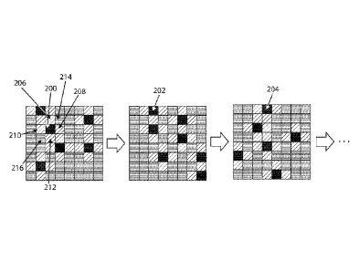
100581 FIG. 2A illustrates a plurality of display pixels going through an
updating,/resetting then edge clearing transition or sequence as described
above. As shown,
16
some of the pixels (e.g., pixels 200, 202, 204) may go through full clearing
transition (e.g., an
iFull pulse is applied of the state I, as illustrated in FIG. 2C); and such
pixels may generate some
edge artifacts, and as a result, its cardinal pixels (e.g., pixels 206, 208,
210 and 212 are cardinal
pixels to pixel 200) will be applied an "edge clearing" transition (i.e., an
iTop pulse or state S, as
illustrated in FIG. 1B). This process can be applied to all the pixels within
the selected group
and their cardinal pixels to ensure all the pixels are free of optical
artifacts, as well as to produce
a uniform graytone throughout the display. Otherwise, the other pixels (e.g.,
pixels 214, 216)
may stay idle (i.e., going through a null transition), as illustrated in FIG.
2D, they remain in an
"empty" state.
[0059] FIG. 3 illustrates a graphical schematic of an inverted top-off
pulse, where such
waveform may be applied to "edge clear" a display pixel, as illustrated above
in FIG. 2B. The
iTop Pulse may be defined by two tunable parameters - the size (impulse) of
the pulse ("iTop
size" ¨ i.e., the integral of the applied voltage with respect to time) and
the "padding" i.e., the
period between the end of the iTop Pulse and end of the waveform ("iTop pad").
These
parameters are tunable and may be determined by the type of display and its
use, the preferred
ranges in number of frames are: size between 1 and 35, and pad between 0 and
50. As stated
above these ranges may be larger if display performance so requires.
[0060] In some embodiments, the iTop Pulse used in dark mode displaying
may be applied
inversely (opposite polarity) to reduce ghosting, edge artifacts and
flashiness when displaying in
light mode as a "top-off pulse". As described in aforementioned U.S. Patent
Publication No.
2013/0194250 a "top-off pulse" applied to a white or near-white pixel drives
the pixel to the
extreme optical white state (and is the opposite polarity of the iTop Pulse,
which drives the pixel
to the extreme optical black state). Typically, the top-off pulse is not used
due to its DC imbalanced
waveform. However, when used in conjunction with the remnant voltage
discharging, the effects
of the DC imbalanced waveform may be reduced or eliminated and the display
performance may
be enhanced. Thus, the top-off pulse is less limited in terms of size and
application. In some
embodiments, the top-off size may be up to 10 frames and may be even greater.
Further, as
described, the top-off pulse may be applied in place of the balanced pulse
pair ("BPP"), which is
a pair of drive pulses of opposing polarities such that the net impulse of the
balanced pulse pair is
substantially zero.
[0061] FIG. 4 is a graphical schematic of an iFull Pulse where voltage is
on the y-axis
and frame number is on the x-axis. Each frame number denotes the time interval
of 1 over the
17
Date Recue/Date Received 2021-01-19
frame rate of the active matrix module. The iFull Pulse may be defined by four
tunable
parameters: 1) the size (impulse) of the iFull Pulse that drives to white (
"pll" parameter); 2) the
"gap" parameter, i.e., the period between the end of the "pll" and the "p12"
parameter; 3) the
size of the iFull Pulse that drives to black ( "p12") and the "padding"
parameter - i.e., the period
between the end of the p12 and end of the waveform ( "pad"). The pll
represents the initial drive
to white state. The p12 represents the drive to black state. The iFull Pulse
improves lightness
error by erasing the edge artifacts that may be created by adjacent pixels not
driving from black
to black. However, the iFull Pulse may introduce significant DC imbalance. The
iFull Pulse
parameters are tunable to optimize the performance of the display by reducing
edge artifact
accumulation with minimum DC imbalance. Although all parameters are tunable
and may be
determined by the type of display and its use, the preferred ranges in number
of frames are:
impulse size between 1 and 25, gap between 0 and 25, size between 1 and 35,
and pad between 0
and 50. As stated above these ranges may be larger if display performance so
requires.
[0062] FIG. 5A illustrates a plurality of pixels going through a series of
update cycles
(e.g., 8 cycles) to update the entire set of pixels, where each update cycle
updates only a portion
of the pixels, as described above. FIG. 5B illustrates an exemplary pixel map
matrix where each
display pixel is programmed to be updated in a particular update cycle. FIG.
5C illustrates an
exemplary algorithm where the pixel map of FIG. 5B may be generated.
[0063] FIG. 6A illustrates an exemplary flow process where a plurality of
pixels may be
firstly mapped out and subsequently updated in a particular update cycle.
Where in step 610 a
desired dithering mask may be chosen, the size of the dithering mask may
depend on design
goals regarding overall display flashness, pixel fatigue and update time. In
step 612, each
display pixel is assigned a numerical value, such that display pixels will be
grouped according
their assigned number and will be updated one group (e.g., 8 groups as
described above) at a
time. Finally in step 614, when the pixels are going through the update phase,
appropriate
waveforms will be applied to the pixels. For example, as discussed above, the
group of pixels
that are chosen to go through the update will be applied an iFull pulse, while
its cardinal
neighbors will be applied an iTop pulse to get rid of the edge artifacts. An
example algorithm
for implementing the process illustrated in FIG. 6A may be as follows:
18
Date Recue/Date Received 2021-01-19
Example of imaging algorithm:
The imaging algorithm specifies:
'I. locations to modify the state in the next waveform state image so
that a special 5-transition
will be used. This transition dears edges that would be created from the
previous text/images as
it transitions to the black background.
2. locations to modify the state in the next waveform state in so
that a .special I-transit, ion
will be used. This transition clears edges that would be created from the
previous all black pixels
transitioning to black pixel adjacent to non-black graytones.
3. locations to modify the state in the next waveform state image so that a
special T-transition
will be used. This transition clears edges that would be created from the
previous text/images as
it transitions to the white background.
4..
locations to modify the state in the next waveform state image so that a
special F-transition
will be used. This transition dears edges that would be created from the
previous all white
pixels transitioning to white pixel adjacent to non-white graytones.
For all pixels i,j) in any order:
if the pixel graytone transition is not W-044 and not B4134 apply
standard transition
Else, if the pixel graytone transition is WW, and at least srT
cardinal neighbors are not making a graytone transition from
WW, apply the F W4W transition.
Else, if the pixel graytone transition is and all fourcardinal
neighbors have a next graytone of white, AND at least one
cardinal neighbor has a current graytone not white, apply the T
W-0 transition.
Else, if the pixel is selected by Active Mask(i,j), apply the B-,13
transition.
Else, if the pixel graytone transition is BB, and at least SIT
cardinal neighbors are not making a graytone transition from
B-0134 apply the I B-*B transition.
Else, if all four cardinal neighbors have a nexy graytone of black, and
with at least one cardinal neighbor has a current graytone not
black, apply the S B-+13 transition
Otherwise use the W-*11 and BB transitions of the waveform table
End
[0064] Alternatively, in some other embodiments, pixels chosen for a full
update or reset
(e.g., pixels 702 and 704) may be instead applied a top-off pulse (e.g., iTop
pulse) instead of a
full clearing pulse (e.g., iFull pulse), and its cardinal pixels may stay idle
or be applied a null
waveform. This setup allows for an even less flashy update of the dark
18a
Date ecue/Date Received 2021-01-19
CA 03054848 2019-08-27
WO 2018/160912
PCT/US2018/020566
background pixels in a dark mode operation. Due to the nature of the ink
particles, applying
only a top-off pulse such as the iTop pulse instead of a full clearing pulse
can produce an
even less flashy update of the display pixels, while still maintain a
relatively consistent
graytone throughout the display (e.g., between the updated pixels 702, 704 and
the its idle
cardinal pixels).
100651 It will be apparent to those skilled in the art that numerous
changes and
modifications can be made in the specific embodiments of the invention
described above
without departing from the scope of the invention. Accordingly, the whole of
the foregoing
description is to be interpreted in an illustrative and not in a limitative
sense.
19