Note: Descriptions are shown in the official language in which they were submitted.
CA 03057068 2019-09-18
WO 2018/022799
PCT/US2017/044023
MULTI-ELECTRODE STRUCTURES FOR MOLECULAR SENSING DEVICES
AND METHODS OF MAKING SAME
CROSS-REFERENCE TO RELATED APPLICATIONS
[0001]
This application claims priority to U.S. Non-Provisional Patent Application
Serial No. 15/220,307, filed July 26, 2016, entitled "Multi-Electrode
Molecular Sensing
Devices and Methods of Making the Same," the disclosure of which is
incorporated herein
by reference in its entirety.
FIELD
[0002] The
present disclosure relates to nanofabrication and nanoelectronics. More
particularly, the present disclosure relates to structures such as device
stacks, and the
fabrication of structures usable in devices for sensing and analyzing
molecules, including
genome sequencing and DNA sequencing.
BACKGROUND
[0003]
Molecular analysis has received an increasing amount of attention in various
fields such as precision medicine or nanotechnology. One example includes the
analysis
of molecules for sequencing genomes. The seminal work of Avery in 1946
demonstrated
that DNA was the material that determined traits of an organism. The molecular
structure
of DNA was then first described by Watson and Crick in 1953, for which they
received the
1962 Nobel Prize in Medicine. This work made it clear that the sequence of
chemical
letters (bases) of the DNA molecules encode the fundamental biological
information.
Since this discovery, there has been a concerted effort to develop means to
actually
experimentally measure this sequence. The first method for systematically
sequencing
DNA was introduced by Sanger in 1978, for which he received the 1980 Nobel
Prize in
Chemistry.
1
CA 03057068 2019-09-18
WO 2018/022799
PCT/US2017/044023
[0004] A basic method for sequencing a genome was automated in a commercial
instrument platform in the late 1980's, which ultimately enabled the
sequencing of the first
human genome in 2001. This was the result of a massive public and private
effort taking
over a decade, at a cost of billions of dollars, and relying on the output of
thousands of
dedicated DNA sequencing instruments. The success of this effort motivated the
development of a number of "massively parallel" sequencing platforms with the
goal of
dramatically reducing the cost and time required to sequence a human genome.
Such
massively parallel sequencing platforms generally rely on processing millions
to billions
of sequencing reactions at the same time in highly miniaturized microfluidic
formats. The
first of these was invented and commercialized by Rothberg in 2005 as the 454
platform,
which achieved thousand fold reductions in cost and instrument time. However,
the 454
platform still required approximately a million dollars and took over a month
to sequence a
genome.
[0005]
Further improvements in quality and accuracy of sequencing, as well as
reductions in cost and time are still needed. This is especially true to make
genome
sequencing practical for widespread use in precision medicine, where it is
desirable to
sequence the genomes of millions of individuals with a clinical grade of
quality.
[0006] While many DNA sequencing techniques utilize optical means with
fluorescence reporters, such methods can be cumbersome, slow in detection
speed, and
difficult to mass produce to further reduce costs. Label-free DNA or genome
sequencing
approaches provide advantages of not having to use fluorescent type labeling
processes
and associated optical systems, especially when combined with electronic
signal detection
that can be achieved rapidly and in an inexpensive way.
[0007] In
this regard, certain types of molecular electronic devices can detect single
molecule, biomolecular analytes such as DNAs, RNAs, proteins, and nucleotides
by
2
CA 03057068 2019-09-18
WO 2018/022799
PCT/US2017/044023
measuring electronic signal changes when the analyte molecule is attached to a
circuit.
Such methods are label-free and thus avoid using complicated, bulky and
expensive
fluorescent type labeling apparatus.
[0008] While current molecular electronic devices can electronically measure
molecules for various applications, they lack the scalability and
manufacturability needed
for rapidly sensing many analytes at a scale of up to millions in a practical
manner. Such
highly scalable methods are particularly important for DNA sequencing
applications,
which often need to analyze millions to billions of independent DNA molecules.
In
addition, the manufacture of current molecular electronic devices is generally
costly due to
the high level of precision needed.
SUMMARY OF THE INVENTION
[0009] In
various embodiments of the present disclosure, a method of manufacturing a
structure usable in a molecular sensor device is described. The method
comprises:
providing a substrate defining a substrate plane with a protrusion protruding
from the
substrate at an angle to the substrate plane; depositing a first electrode
layer in an
orientation along a side of the protrusion to form a first electrode sheet at
the angle to the
substrate plane; depositing an inner dielectric layer on the first electrode
layer to form an
inner dielectric sheet at the angle to the substrate plane; depositing a
second electrode layer
on the inner dielectric layer to form a second electrode sheet at the angle to
the substrate
plane, wherein the first electrode sheet and the second electrode sheet form a
pair of
electrode sheets spaced apart by the inner dielectric sheet between the first
electrode sheet
and the second electrode sheet; depositing an outer dielectric layer on the
second electrode
layer to form an outer dielectric sheet at an angle to the substrate plane;
repeating the
depositing of the first electrode layer, the inner dielectric layer, the
second electrode layer,
and the outer dielectric layer at least once to form spaced apart pairs of
electrode sheets
3
CA 03057068 2019-09-18
WO 2018/022799
PCT/US2017/044023
with an inner dielectric sheet between each electrode sheet in the pair of
electrode sheets
and an outer dielectric sheet between each pair of electrode sheets;
planarizing the pairs of
electrode sheets, the inner dielectric sheets, and the outer dielectric
sheets; and removing
an exposed end portion of each inner dielectric sheet to form grooves in each
inner
dielectric sheet descending from the planarized edge toward the substrate.
[0010] In
certain examples, each inner dielectric layer is deposited with a first
thickness, each outer dielectric sheet is deposited with a second thickness,
and the second
thickness is at least one order of magnitude greater than the first thickness.
[0011] In
some aspects, the method may further comprise attaching a mechanically
supportive block material adjacent a stack formed by the deposited first
electrode layers,
inner dielectric layers, second electrode layers, and outer dielectric layers,
prior to the step
of planarizing. The block material can lend support to the structure during
planarization.
[0012] In
various examples, the inner dielectric sheets and the outer dielectric sheets
comprise different dielectric materials. In some instances, differing
materials allows for
selective etching of the exposed edges of the inner dielectric sheets in the
presence of the
exposed outer edges of the outer dielectric sheets, such as to form the
grooves.
[0013] In
various embodiments, the forming of the groove in each inner dielectric sheet
comprises: removing portions of the inner dielectric sheet; and stopping
further removal of
the inner dielectric sheet based on an electrical, capacitance, or optical
measurement
between the pair of electrode sheets.
[0014] In
some aspects, the method of manufacturing may further comprise depositing
a dielectric cover layer at an angle or perpendicular to the plurality of
pairs of electrode
sheets opposite the substrate to define a gap exposing a portion of the spaced
apart pairs of
electrode sheets. Further, the method may comprise roughening an exposed edge
of each
4
CA 03057068 2019-09-18
WO 2018/022799
PCT/US2017/044023
electrode sheet, such as to facilitate attachment of metals or molecules onto
the exposed
edges.
[0015] In
adapting structures for use in sensor devices, the method may further
comprise connecting a plurality of lead conductors to the spaced apart pairs
of electrode
sheets with each lead conductor connected to a respective electrode sheet,
wherein each
lead conductor diverges in width as the lead conductor extends away from an
edge of the
electrode sheet. In certain examples, the method may further comprise
depositing a gate
electrode parallel to the substrate plane and perpendicular to an electrode
plane defined by
an electrode sheet in the spaced apart pairs of electrode sheets. Also in
certain
embodiments, the method may further comprise forming a plurality of channels,
each
channel arranged to introduce a fluid to exposed portions of at least two
pairs of electrode
sheets.
[0016] In
other embodiments of the present disclosure, a method of manufacturing a
device stack usable in a molecular sensor is disclosed. The method comprises:
providing a
first outer dielectric layer; depositing a first electrode layer on the first
outer dielectric
layer; depositing an inner dielectric layer on the first electrode layer;
depositing a second
electrode layer on the inner dielectric layer; and depositing a second outer
dielectric layer
on the second electrode layer; slicing through the stack at least once at an
angle to the
layers in the stack to form at least two chips from the sliced portions of the
stack; and
attaching the chips to a substrate so that the sliced portions of the first
electrode layer and
the second electrode layer form a plurality of pairs of electrode sheets at an
angle to a
substrate plane defined by the substrate, and so that the sliced portions of
the inner
dielectric layer forms a plurality of inner dielectric sheets with each inner
dielectric sheet
between each electrode sheet in each pair of electrode sheets. In certain
aspects, forming
the device stack further includes repeating the deposition of the first
electrode layer, the
5
CA 03057068 2019-09-18
WO 2018/022799
PCT/US2017/044023
inner dielectric layer, the second electrode layer, and the second outer
dielectric layer at
least once so that each chip of the plurality of chips includes multiple pairs
of electrode
sheets.
[0017] In
various examples, the inner dielectric layer has a first thickness and the
second outer dielectric layer has a second thickness at least one order of
magnitude greater
than the first thickness. Further, the inner dielectric layers and the outer
dielectric layers
may comprise different dielectric materials.
[0018] In
various embodiments, the method may further comprise forming a groove
located on an exposed end portion of each inner dielectric sheet.
Additionally, the method
may further comprise depositing a dielectric cover layer at an angle or
perpendicular to the
plurality of pairs of electrode sheets opposite the substrate to define a gap
exposing a
portion of the plurality of pairs of electrode sheets. In some examples, the
method
comprises roughening an exposed edge of each electrode sheet.
[0019] In
various aspects, the method further comprises depositing a gate electrode
parallel to the substrate plane and perpendicular to an electrode plane
defined by an
electrode sheet in the plurality of pairs of electrode sheets. In some
examples, the method
may further comprise forming a plurality of channels, each channel arranged to
introduce a
fluid to exposed portions of at least two pairs of electrode sheets of the
plurality of pairs of
electrode sheets.
[0020] In various
embodiments of the present disclosure, a structure usable in a
molecular sensor device is described. Such structures can be fabricated with
the methods
of manufacturing described herein. In various examples, a structure usable in
a molecular
sensor device comprises, a substrate defining a substrate plane; spaced apart
pairs of
electrode sheets attached on an edge of the electrode sheet to the substrate
at an angle to
the substrate plane; an inner dielectric sheet disposed between the electrode
sheets in each
6
CA 03057068 2019-09-18
WO 2018/022799
PCT/US2017/044023
pair of electrode sheets; and an outer dielectric sheet disposed between
spaced apart pairs
of electrode sheets, wherein an edge of each electrode sheet, inner dielectric
sheet and
outer dielectric sheet opposite the substrate are coplanar and substantially
parallel to the
substrate plane.
[0021] In various
examples, each inner dielectric sheet has a first thickness, and
wherein each outer dielectric sheet has a second thickness at least one order
of magnitude
greater than the first thickness.
[0022] In
various examples, the structure comprises a groove located on an exposed
end portion of each inner dielectric sheet opposite the substrate. Further in
some examples,
the inner dielectric sheets and the outer dielectric sheets comprise different
dielectric
material. For example, inner dielectric sheets comprising SiO2 may be
selectively etched in
the presence of outer dielectric sheets comprising A1203, such as to form
grooves in
exposed end portions of the inner dielectric sheets.
[0023] In
some examples, the structure may further comprise dielectric cover layers
covering portions of the edges of the spaced apart pairs of electrodes
opposite the
substrate, the dielectric cover layers spaced apart by a gap in which a
portion of the spaced
apart pairs of electrodes are exposed. The gap in certain aspects may be
between about 2
nm to about 40 nm in width.
[0024] In
certain aspects, an exposed edge of each electrode sheet opposite the
substrate may been roughened, such as to improve bonding of other metal
deposits or
molecules onto the exposed edges of the electrode sheets.
[0025] In
various embodiments, the structure may further comprise: a plurality of lead
conductors, each lead conductor of the plurality of lead conductors extending
from an
electrode sheet of the plurality of pairs; and a plurality of contacts, each
contact of the
plurality of contacts in electrical communication with a lead conductor of the
plurality of
7
CA 03057068 2019-09-18
WO 2018/022799
PCT/US2017/044023
lead conductors, wherein each lead conductor of the plurality of lead
conductors diverges
in width from an edge of the electrode sheet to the contact. The structure may
also
comprise a gate electrode parallel to the substrate plane and perpendicular to
an electrode
plane defined by an electrode sheet in the spaced apart pairs.
[0026] In various
examples, the structure further comprises a plurality of channels, each
channel of the plurality of channels arranged to introduce a fluid to exposed
portions of at
least two pairs of electrode sheets of the plurality of pairs. In some
examples, the structure
comprises a portion of a molecular sensor used to detect at least one of a DNA
molecule, a
nucleotide, an antibody molecule, and a protein molecule by measuring an
electronic
signal in the molecular sensor. Such a molecular sensor may be used for genome
sequencing.
BRIEF DESCRIPTION OF THE DRAWINGS
[0027] The
features and advantages of the embodiments of the present disclosure will
become more apparent from the detailed description set forth below when taken
in
conjunction with the drawings. The drawings and the associated descriptions
are provided
to illustrate embodiments of the disclosure and not to limit the scope of what
is claimed.
[0028]
FIG. 1A is a cross section view showing fabrication of a molecular sensor by
sequentially depositing tri-layer thin film device stacks using a low
deposition angle and a
sacrificial top layer according to an embodiment.
[0029] FIG. 1B is a
cross section view showing further fabrication of the molecular
sensor of FIG. 1A.
[0030]
FIG. 1C is a cross section view of the molecular sensor of FIGS. 1A and 1B
after fabrication.
8
CA 03057068 2019-09-18
WO 2018/022799
PCT/US2017/044023
[0031]
FIG. 2A is a cross section view showing fabrication of a molecular sensor by
sequentially depositing tri-layer thin film device stacks using a low
deposition angle and
detachable shades according to an embodiment.
[0032]
FIG. 2B is a cross section view showing further fabrication of the molecular
sensor of FIG. 2A.
[0033]
FIG. 2C is a cross section view of the molecular sensor of FIGS. 2A and 2B
after fabrication.
[0034]
FIG. 3 is a flowchart for a manufacturing process of the molecular sensor of
FIG. 1C or FIG. 2C according to an embodiment utilizing low incident angle
oblique
deposition.
[0035]
FIG. 4A is a cross section view showing fabrication of a molecular sensor by
sequentially depositing tri-layer thin film device stacks using a high
deposition angle
according to an embodiment.
[0036]
FIG. 4B is a cross section view of the molecular sensor of FIG. 4A after
fabrication.
[0037]
FIG. 5 is a flowchart for a manufacturing process of the molecular sensor of
FIG. 4B according to an embodiment utilizing high incident angle oblique
deposition.
[0038]
FIG. 6 is a flowchart for an additional manufacturing process according to an
embodiment.
[0039] FIG. 7A is a
cross section of a molecular sensor showing the deposition of a
mask line during the manufacturing process of FIG. 6.
[0040]
FIG. 7B is a cross section of the molecular sensor of FIG. 7A after depositing
a
dielectric cover layer and removing the mask line of FIG. 7A.
[0041]
FIG. 8 is a cross section of the molecular sensor of FIG. 7B illustrating the
roughening of an exposed portion of electrode sheets according to an
embodiment.
9
CA 03057068 2019-09-18
WO 2018/022799
PCT/US2017/044023
[0042]
FIG. 9 is a top view of a molecular sensor with diverging lead conductors
according to an embodiment.
[0043]
FIG. 10 is a top view of the molecular sensor of FIG. 9 with a gate electrode
according to an embodiment.
[0044] FIG. 11 is a
top view of a molecular sensor with channels for introducing a fluid
to pairs of electrode sheets according to an embodiment.
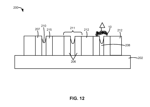
[0045]
FIG. 12 depicts a molecular sensor manufactured by forming a stack of layers
and slicing through the stack according to an embodiment.
[0046]
FIG. 13 is a flowchart for a manufacturing process of the molecular sensor of
FIG. 12 according to an embodiment.
[0047]
FIG. 14A is a cross section of a stack of layers during the manufacturing
process of FIG. 13.
[0048]
FIG. 14B illustrates the slicing of the stack of FIG. 14A to form chips during
the
manufacturing process of FIG. 13.
[0049] FIG. 14C is a
cross section view showing the placement of a chip from FIG.
14B on a substrate during the manufacturing process of FIG. 13.
[0050]
FIG. 15 illustrates the placement of multiple chips on a substrate according
to an
embodiment.
[0051]
FIG. 16 illustrates the placement of a dielectric cover layer on the multiple
chips
of FIG. 15 according to an embodiment.
[0052]
FIG. 17 is a top view of a molecular sensor with diverging lead conductors
according to an embodiment.
[0053]
FIG. 18 is a top view of a molecular sensor with channels for introducing a
fluid
to pairs of electrode sheets according to an embodiment.
CA 03057068 2019-09-18
WO 2018/022799
PCT/US2017/044023
[0054]
FIGS. 19A-19C illustrate embodiments of structures available by OAD and
planarization steps.
[0055] FIGS. 20A and 20B provide TEM and STEM images of a structure in
accordance with the present disclosure.
DETAILED DESCRIPTION
[0056] In
the following detailed description, numerous specific details are set forth to
provide a full understanding of the present disclosure. It will be apparent,
however, to one
of ordinary skill in the art that the various embodiments disclosed may be
practiced
without some of these specific details. In other instances, well-known
structures and
techniques have not been shown in detail to avoid unnecessarily obscuring the
various
embodiments.
[0057] As
used herein, the term "structure" refers generally to physical constructs
comprising at least one of a substrate layer, an electrode layer, or a
dielectric layer, in any
combination, such as formed by depositing metal and/or dielectric layers onto
a substrate.
A "structure" herein may be a part of a molecular sensor or part of a
molecular electronics
component or any other device. In some instances, a "structure" herein can be
converted
into a working molecular sensor by disposing a biomolecule or other molecule
across a
pair of electrodes in a structure, amongst other processes. In some instances,
a structure,
e.g. comprising alternating electrode and dielectric layers on a substrate,
may also be
referred to as a structure usable in, or usable for, a molecular sensor.
[0058] As
used herein, the term "device stack" is an embodiment of a "structure," and
generally refers to a structure having multiple layers of material comprising
metal and
dielectric layers. In a non-limiting example, a device stack comprises a three-
layer (or tri-
layer) arrangement further comprising a dielectric layer sandwiched between
two electrode
layers.
11
CA 03057068 2019-09-18
WO 2018/022799
PCT/US2017/044023
[0059] As used herein, oblique angle deposition, or "OAD," refers to
the process of
depositing material such as a metal at an incident angle less than 90
relative to a planar
substrate receiving the deposition. Normal deposition generally refers to
deposition of
materials orthogonal (90 ) to a substrate plane, which necessarily creates
layers that are
co-planar with a top surface of the substrate. OAD, on the other hand,
comprises
deposition onto a substrate at an angle less than 90 , (including at 0 or
"horizontally"),
such that vertical surfaces protruding from a substrate plane can also receive
deposition of
materials. The definition of OAD is extended herein to include 0 (also
referred to as
"horizontal" or "sideways") deposition, which can result in no material being
deposited
onto the top plane of a substrate sheet, but rather only deposition on the
edge of the
substrate facing the deposition stream, and on the surfaces of any protrusions
emanating
from the substrate that face the deposition stream
[0060] Low angle deposition
[0061] The cross-sectional views of FIGS. 1A to 1C illustrate
embodiments of
intermediate structures 100 obtained by executing various steps of the
fabrication process
of the present disclosure, such as by using low angle (from about 0 to about
20 ) or 0
(horizontal) incident film deposition of alternating thin films and thick
films, relative to a
substrate plane 103. As illustrated for example in FIG. 1A, a tri-layer thin
film structure or
device stack 111 may be formed by sequential deposition of a first electrode
sheet 107, an
inner dielectric sheet 108, and a second electrode sheet 115. The structure
100 in FIG. 1A
is fabricated by deposition of a thicker outer dielectric sheet 112 and then
by a repetition of
the deposition of the three layers first electrode sheet 107, inner dielectric
sheet 108 and
second electrode sheet 115, to form multiple adjacent tri-layer device stacks
111 with
thicker outer dielectric sheets 112 as separators, in accordance to a non-
limiting
embodiment.
12
CA 03057068 2019-09-18
WO 2018/022799
PCT/US2017/044023
[0062] As
shown in FIGS. 1A to 1C, structure 100 includes a supporting substrate 102
with a protrusion 104 protruding from the substrate 102 at an angle to a
substrate plane
103 defined by the substrate 102. The protrusion 104 may be disposed
substantially
perpendicular to the substrate plane 103, or at another angle to the substrate
plane 103 such
as from about 90 to about 45 . In various embodiments, the protrusion 104 may
appear as
a block of material on the substrate 102. The supporting substrate 102 may
comprise, for
example, 5i02 or Si having a 5i02 coating. In the example of FIG. 1A-1C, the
protrusion
104 comprises a block that extends from the substrate 102 perpendicular to the
substrate
plane 103. In other implementations, the protrusion 104 may protrude from the
substrate
102 at a different angle, such as for example, a 45 or 60 angle relative to
the substrate
plane 103.
[0063] The
protrusion 104 may comprise, for example, a dielectric material such as
5i02, A1203, or MgO. In various examples, the combination of substrate 102 and
protrusion 104 can be formed by removing (e.g., ablating) a portion of a
larger block of
substrate material to create the step-like feature, or by attaching the
protrusion 104 (e.g., a
block of dielectric material) onto the substrate 102. The protrusion 104 can
provide
structural support for the depositing of dielectric and/or electrode layers at
an angle to the
substrate plane 103.
[0064]
FIG. 1A illustrates an embodiment of a structure 100 resulting from thin film
and thick film deposition process steps. The deposits are made onto the step-
like
combination of protrusion 104 and substrate 102. In this embodiment,
sacrificial top and
side layers 119 are included to enable sideways deposition of multiple tri-
layer device
stacks 111. In the example of FIG. 1A, the deposition angle can be horizontal
as shown by
the large arrows on the right side of FIG. 1A, or may be within about plus or
minus 20
from the horizontal plane 103. A first conductive electrode sheet 107
deposited by the
13
CA 03057068 2019-09-18
WO 2018/022799
PCT/US2017/044023
OAD process comprises a thin film deposited at a sideways or low deposition
angle. The
process is continued by deposition of an inner dielectric sheet 108, and then
a second
electrode sheet 115. This process can be repeated to form many device stacks
111, each
including a pairs of electrode sheets 106 with an inner dielectric sheet 108
between the
pair of electrode sheets 106, with each device stack 111 separated by a
thicker outer
dielectric sheet 112 deposited between repeating cycles of deposition of the
device stack
layers.
[0065] A
thicker dielectric sheet 112 is deposited between each tri-layer device stack.
FIGS. 1A-1C, along with all other drawing figures herein depicting structures,
should not
be interpreted literally as to the sizes of the various elements. For example,
the relative
size shown for the tri-layer device stacks 111 and separator outer dielectric
sheets 112 may
be somewhat exaggerated to better illustrate the features of the tri-layer
device stacks 111.
In this regard, the cross sectional width of the tri-layer device stacks in
some embodiments
may be less than about 50 nm.
[0066] FIG. 1B
illustrates an embodiment of a structure 100 further comprising a
mechanically supportive block material 123 added to facilitate polishing of
the material
from the top and planarizing the structure along plane 117. Block material 123
can
comprise, for example, an oxide or a precursor of an oxide (e.g., hydrogen
silsesquioxane,
or "HSQ").
[0067] FIG. 1C shows
a cross-section of an embodiment of a structure 100. Such a
structure 100 may be obtained by planarizing the structure in FIG. 1B across
plane 117.
The planarization across plane 117 in FIG. B may be at a level higher or lower
than the
intersection of the protrusion 104 and the sacrificial material 119. In
various examples, the
planarization across plane 117 removes sacrificial material 119 in its
entirety.
14
CA 03057068 2019-09-18
WO 2018/022799
PCT/US2017/044023
[0068]
FIG. 2A demonstrates use of detachable top and side shades 121 to help enable
sideways or low angle deposition of multiple tri-layer thin film device stacks
111. These
shades 121 act as barriers or shields to the incident deposition stream, and
are layered on
their ends by the successive depositions as illustrated. In various examples,
a shade 121
replaces the need for a sacrificial material 119 (see FIGS. 1A and 1B). As
shown in FIG.
2B, a portion of the protrusion 104 is effectively blocked from low angle or
horizontal
OAD by the shade 121. The structure 100 is produced by layering a first
conductive
electrode sheet 107 as a thin film by low deposition angle OAD, followed by
deposition of
an inner dielectric thin film sheet 108, and then a second electrode sheet
115. This process
is repeated to form multiple device stacks 111, with a thicker dielectric
separator sheet 112
deposited between adjacent tri-layer stacks 111.
[0069]
FIG. 2B illustrates an embodiment of a structure 100 after the addition of a
mechanically supportive block material 123, which can comprise an oxide or
precursor of
an oxide (e.g., HSQ), to the structure of FIG. 2A after removal of the shades
121. As
illustrated, the supportive block material 123 may be attached to the
substrate 102 and may
occupy the regions above the substrate that were previously shielded from
deposition of
the various layers. In some examples, the supportive block material 123 may be
disposed
in the region under the multiple device stacks and the region adjacent to the
last deposited
layer. The supportive block material 123 can facilitate planarization and
polishing of the
structure from the top, across plane 117. FIG. 2C illustrates a cross-
sectional view of a
structure 100 obtained by planarizing the structure of FIG. 2B along plane
117.
[0070] The
structures 100 usable in molecular sensors, such as shown in the examples
of FIGS. 1C and 2C, utilize a unique geometry of electrodes in a vertically
aligned or near
vertically aligned tri-layer sheet configuration. One notable difference
between the
structure of FIG. 1C and the structure of FIG. 2C is that in the structure of
FIG. 1C, the
CA 03057068 2019-09-18
WO 2018/022799
PCT/US2017/044023
electrode layers and inner and outer dielectric layers extend all the way to
the substrate
102. In structure 100 of FIG. 2C, they do not because of the intervening block
material
123.
[0071]
When used in various sensors, the sheet geometry of the electrically
conductive
electrodes as shown in these structures ordinarily allows for a low electrical
resistance of
the sensor electrodes, enabling high signal-to-noise ratios, with accurate
dimensional
control and ease of scale-up fabrication at a relatively low cost. This
configuration can
facilitate the packing of high-density device arrays into relatively small
device surface
areas, allowing the manufacture of a compact multiple device assembly. The
sequential
deposition of a first conductor layer, an inner dielectric layer, and a second
conductor layer
can be repeated many times, depositing the outer dielectric layer onto each
second
conductor layer prior to the next repeat of the device stack layers. In this
regard, this
sequence of depositions may be repeated from 2 to 10,000 times or more to
produce an
array of at least 2 to tens of thousands of parallel devices.
[0072] A tri-layer
device stack 111 in various embodiments of the structures herein can
include highly electrically conductive metallic electrode sheets in a vertical
or near-
vertical configuration. Other implementations can include a tilted angle
orientation of the
layers of a device stack of up to about 60 from vertical. In some examples,
layers of a
device stack are tilted from vertical at no more than about 20 . Each pair of
electrode
sheets 106 is separated in the device stack 111 by a dielectric sheet layer
material 108 that
can be selected from oxides (e.g., SiO2, Al2O3, MgO, CaO, refractory oxide,
rare earth
oxide, or a mixture of oxides), nitrides (e.g., AN, Si3N4, refractory nitride,
rare earth
nitride or a mixture of nitrides), fluoride, oxyfluoride, or oxynitride.
[0073] The
material for the electrode sheets 107 and 115 in each device stack 111 may
be selected from high-conductivity metals or alloys, including, but not
limited to, Au, Pt,
16
CA 03057068 2019-09-18
WO 2018/022799
PCT/US2017/044023
Pd, Ag, Os, Ir, Rh, Ru and their alloys. The dimensions of the exposed
electrode sheet
edges on the structure top surface after planarization can have a thickness
(or width) of, for
example, from about 1 to about 100 nm. In various embodiments, the electrode
sheets 107
and 115 (e.g. in FIGS. 1A and 2A) can be deposited to a thickness of from
about 1 to about
40 nm, or from about 5 to about 15 nm, with the height of a vertical or near-
vertical
electrode sheet being at least about 100 p.m tall (as measured from the
substrate 102 top
surface up to the level of planarization). In other examples, the height of
the electrode
sheets are at least about 1,000 p.m tall, or at least about 10,000 p.m tall.
Accordingly, the
aspect ratio for an electrode sheet, (in terms of height to thickness), is at
least about 10,000
or at least about 100,000. With this aspect ratio, an electrode sheet herein,
standing
vertically or nearly vertical with respect to the substrate plane 103, will
necessarily have a
top edge that is opposite the substrate 102. When a vertically disposed
electrode sheet is
planarized across a plane substantially parallel to the substrate plane 103,
the top edge of
the electrode sheet will necessarily be substantially parallel to the
substrate plane 103.
After planarization, exposed top edges of the electrode sheets, the inner
dielectric sheets,
and the outer dielectric sheet, appear as parallel strips on the planarized
top surface of the
structure.
[0074] In other embodiments, a thin adhesion promoting layer may be deposited
at the
interface between the electrode sheets and the inner dielectric sheet to
improve the
adhesion at the interface. For example, an about 1 to about 5 nm thick film
may be
deposited at the interface, wherein the film may comprise a material such as
Ti, Cr, Al, Zr,
Mo, Nb, Ta, or Hf.
[0075] The
thickness of the exposed end portion of an inner dielectric sheet 108
deposited between the two electrode sheets on the structure's top surface
after
planarization may be from about 1 to about 40 nm. In some examples, the
thickness of the
17
CA 03057068 2019-09-18
WO 2018/022799
PCT/US2017/044023
exposed end portion of the inner dielectric layer after planarization may be
from about 5 to
about 15 nm. In some embodiments, the thickness of the inner dielectric sheets
108 may
be less than about 10 nm. The height of a vertical or near-vertical dielectric
sheet 108 may
be at least about 100 p.m tall. In other examples, the height is at least
about 1,000 p.m tall
or at least about 10,000 p.m tall. Accordingly, the aspect ratio of the inner
dielectric layer
sheet, (in terms of height to thickness), is at least about 10,000 or at least
about 100,000.
[0076] The
dimension of each outer dielectric layer 112 separating neighboring tri-
layer device stacks 111, may have a width of at least about 500 to at least
about 20,000
nm, or about one order of magnitude thicker than the thickness of any one
inner dielectric
sheet separating first and second electrodes in a device stack. In various
examples, a
thickness for an outer dielectric layer 112 can be, for example, in the range
of from about
500 to about 5,000 nm. A separation between adjacent tri-layer device stacks
111 of about
500 to about 5,000 nm reduces electrical, inductive, capacitive, or other
interferences.
[0077]
Various embodiments of the structure 100 can be fabricated using a low
incident
angle OAD of layers, such as at a deposition angle of 00 to less than about 20
from the
substrate plane (see substrate plane 103 in FIG. 1A for example). In the
example process
of FIG. 3, a low incident angle OAD is used with one or more sacrificial
layers (e.g.,
sacrificial layers 119 in FIG. 1A) and/or detachable shades (e.g., detachable
shades 121 in
FIG. 2A) to help prevent deposition of the electrode and dielectric layers on
certain
surfaces. The sacrificial layers and/or detachable shades are later removed
after the
electrode and dielectric sheets have been formed at the desired angle to the
substrate plane
103.
[0078] In
the example of FIG. 1A, a series of film depositions are performed at a
deposition angle of 0 to less than about 20 from the substrate plane 103.
The sacrificial
layer 119 on a surface of the protrusion 104 opposite the substrate 102 is
disposable upon
18
CA 03057068 2019-09-18
WO 2018/022799
PCT/US2017/044023
planarization. In some examples, the sacrificial layer 119 can include a
slight extension
off an edge of the protrusion 104 to help prevent deposition above the top
surface of the
protrusion 104.
[0079]
FIG. 5, discussed below, provides an alternative embodiment of a process that
includes performing the multilayer deposition at a higher oblique incident
angle prior to
planarization. The higher oblique incident angle for multilayer OAD can be
performed,
for example, at any angle in the range of about 20 to about 70 from the
substrate plane
103, such as between about 30 and about 60 . Utilizing OAD without a
sacrificial layer
as in the process of FIG. 5, the surface of the protrusion 104 opposite the
substrate 102 is
also covered with multilayer thin films, (e.g., as illustrated in FIG. 4A).
Nonetheless, a
planarization polishing process removes these film depositions on the surface
of the
protrusion 104 so as to achieve a structure as in FIG. 4B. In some instances,
the very top
layer of the protrusion 104 is sacrificed in the planarization that removes
all of the layers
previously deposited on the protrusion 104.
[0080] FIG. 3
illustrates a flowchart of an exemplary fabrication process according to
the present disclosure. As illustrated in the flowchart of FIG. 3, step 302
comprises
providing a substrate (such as the substrate 102 depicted throughout the
various
embodiments). As discussed, a substrate 102 further comprises a major surface
that defines
substrate plane 103. The substrate plane can be defined by being parallel with
a major
surface of the substrate, such as a top or bottom surface used for supporting
dielectric
and/or electrode layers.
[0081] In
step 304, a protrusion (e.g., a protrusion 104 depicted throughout the various
embodiments) is attached to the substrate 102, or in alternative embodiments,
the
protrusion is formed by removing one or more portions of a larger substrate,
generating a
cut-out "step" in an initially thicker supporting substrate. In various
examples, a dielectric
19
CA 03057068 2019-09-18
WO 2018/022799
PCT/US2017/044023
material in a block or other shape may be attached to the substrate to form
the protrusion at
the desired angle to the substrate plane. As noted above, the protrusion
(regardless if
attached material or formed by cutting out a step in a thicker substrate)
protrudes from the
substrate plane at an angle, such as about 90 .
[0082] With
continued reference to FIG. 3, step 305 comprises the placement of one or
more sacrificial layers and/or detachable shades on a side of a structure
targeted for OAD,
(e.g., detachable shades 121 in FIG. 2A) and/or on a surface of the protrusion
opposite the
substrate (e.g., the top sacrificial layer 119 in FIG. 1A). As noted above,
the sacrificial
layer may extend beyond an edge of the protrusion 104. The sacrificial layer
can include,
for example, a physically removable plate, or a dissolvable polymer layer,
such as acetone-
dissolvable (poly)methyl methacrylate (PMMA), common in lift-off processing in
semiconductor fabrication. The detachable shade can include, for example, a
detachable
metallic, ceramic, or polymer material.
[0083] In
step 306, a first electrode layer is deposited on the substrate. In various
embodiments, at least a portion of the first electrode layer is deposited
against an exposed
side of a protrusion from the substrate, thereby resulting in a first
electrode sheet (e.g., first
electrode sheet 107 in FIG. 1A or in FIG. 2A) at an angle to the substrate
plane equaling
the angle between the protrusion and the substrate. In other implementations,
a dielectric
layer, (e.g., an outer dielectric layer as described herein) may be deposited
against the
protrusion first, before deposition of the first electrode layer and
subsequent layers.
[0084] In
the embodiment depicted in the flowchart of FIG. 3, an inner dielectric layer
is deposited in step 308 on the first electrode layer previously deposited in
step 306. As
shown in the examples of FIGS. 1A and 2A, at least a portion of the inner
dielectric layer
is deposited against the protrusion 104 to form the inner dielectric sheet 108
at the same
orientation of the protrusion to the substrate plane 103. As with the first
electrode layer
CA 03057068 2019-09-18
WO 2018/022799
PCT/US2017/044023
deposited in step 306, OAD can be used to deposit the inner dielectric layer
at an angle to
the substrate plane. Complementary metal-oxide semiconductor (CMOS) processes,
such
as OAD, can ordinarily allow for the inner dielectric layer to be deposited
with an accurate
and repeatable thickness.
[0085] In some
implementations, a thin adhesion enhancing layer may be deposited on
the first electrode layer before and/or after depositing the inner dielectric
layer to improve
adhesion of the layers. In various examples, an about 1 to about 5 nm thick
film material
is deposited at the interface using a material. Such film material may
comprise, for
example, Ti, Cr, Al, Zr. Mo, Nb, Ta, or Hf.
[0086] In step 310
of the process depicted in FIG. 3, a second electrode layer is
deposited on the inner dielectric layer to form a second electrode sheet
(e.g., second
electrode sheet 115 in FIGS. 1A and 2A) at the same angle to the substrate
plane as the
prior layers, using, for example, OAD. Upon completion of step 310, a device
stack is
formed, which comprises a first electrode sheet and a second electrode sheet
arranged as a
pair of electrode sheets, with the inner dielectric sheet disposed between the
pair of
electrode sheets.
[0087] In
step 312, an outer dielectric layer is deposited on the second electrode layer
to form an outer dielectric sheet at an angle to the substrate plane. With
reference to the
examples in FIGS. 1A and 2A, the outer dielectric layer is deposited on the
second
electrode layer to form the outer dielectric sheet 112 at the same angle to
the substrate
plane 103 as per the previous layers. In some implementations, the outer
dielectric layer
may have a different thickness than other previously deposited outer
dielectric layers if, for
example, it comprises the final outer dielectric layer. Such a thicker
terminal outer
dielectric layer facilitates packaging of the structure within a larger array
of device stacks,
and/or to provide a greater exterior insulation to an overall array.
21
CA 03057068 2019-09-18
WO 2018/022799
PCT/US2017/044023
[0088] In
step 314, it is determined whether a final number of pairs of electrode sheets
has been reached. In some implementations, the final number of pairs of
electrode sheets
may be as few as one pair of electrode sheets (i.e., one device stack). For
two or more
pairs of electrode sheets, the sub-process comprising steps 306 to 312 is
repeated at least
once to provide for at least two pairs of electrode sheets. In some
implementations, the
final number of pairs of electrode sheets may be as large as several thousand
pairs of
electrode sheets for example. The final number of pairs of electrode sheets
desired may
depend on the design considerations for a sensor being manufactured from the
fabricated
structures, such as a desired testing speed, a type of molecule to be
analyzed, or a desired
footprint for the sensor, and other considerations.
[0089] If
the final number of pairs of electrode sheets has not been reached in step
314,
the process returns to step 306 to deposit another first electrode layer
against a side of the
protrusion to form another first electrode sheet at an angle to the substrate
plane. On the
other hand, if the final number of pairs of electrode sheets has been reached
in step 314,
then the process proceeds to step 315 that comprises the removal of
sacrificial layers or
detachable shades that were added in step 305, discussed above. The
sacrificial layer can,
for example, be physically removed or removed by dissolution. The detachable
shade can
be physically removed. In one example, the sacrificial layer is dissolved
using a liquid, as
in lift-off processing.
[0090] At least one
mechanically supportive block material is also added in step 315,
such as with a gap-filling curable polymer. A mechanically supportive block
material may
be attached adjacent to the deposited multilayer stack (e.g., block 123 added
to the right of
the deposited layers shown in FIGS. 1B and 2B). In some implementations, this
is
accomplished by attaching a block of ceramic material or polymer material, or
by
depositing a polymer material and subsequently curing the polymer. The space
between
22
CA 03057068 2019-09-18
WO 2018/022799
PCT/US2017/044023
the added supporting block and the previously deposited multilayers can be
filled with a
UV-curable, electron beam curable, or thermally curable polymer such as PMMA
or
hydrogen silsesquioxane (HSQ) resist. The HSQ resist layer deposited can be
hardened by
additional thermal curing to be close to the hardness of SiO2 type material.
The
mechanically supportive block material can be added to facilitate subsequent
planarization,
as in optional step 316, or to provide support for handling, such as during a
subsequent
packaging process of the structure 100.
[0091]
Optional step 316 includes planarizing the pairs of electrode sheets, the
inner
dielectric sheets, and the one or more outer dielectric sheets formed from the
previous
repetitive steps, as necessary, of sub-process steps 306 to 312. The step of
planarizing
may comprise, for example, chemical-mechanical planarization (CMP) polishing,
focused
ion beam (FIB) etching, or (poly)methylmethacrylate (PMMA) or HSQ filling and
subsequent "etching back" by reactive ion etch (RIE). After the repeated
deposition of
thin film and thick film electrodes and dielectric layers, the mechanically
supportive block
material added and cured in step 315, such as a SiO2 material or a precursor
of SiO2 (e.g.,
HSQ), can provide mechanical support of the structure during planarization.
The location
of the planarization on the structure may be, for example, along plane 117
shown in FIGS.
1B or 2B, below the top surface of the protrusion 104. In other
implementations, such as
when deposition onto the top of the protrusion is shielded, planarization can
take place just
below the top surface of the protrusion 104 so as to remove the top surface of
the
protrusion, the electrode sheets, and the various inner and outer dielectric
sheets, to expose
the edges of the layers and level all of them substantially planar with a top
surface of the
protrusion 104. In various embodiments, planarization results in a structure
having a top
surface substantially parallel to the substrate plane 103.
23
CA 03057068 2019-09-18
WO 2018/022799
PCT/US2017/044023
[0092] In certain examples, step 316 in FIG. 3 may be omitted when a shade
extends far
enough over an edge of the protrusion to prevent unwanted deposition on the
top of the
protrusion. In such an example, removal of the shade in step 315 may result in
the
exposed top surfaces of the pairs of electrode sheets substantially parallel
without the need
for planaraization.
[0093] High angle deposition
[0094]
With reference now to FIG. 4A, a cross-sectional view of a structure 100
formed
by various embodiments of the fabrication method is illustrated. The structure
100
comprises device stacks further comprising electrode pair sheets 107 and 115
separated by
inner dielectric layer 108. In this embodiment, the structure 100 is
fabricated by
sequentially depositing tri-layer thin film device stacks using a high angle
OAD. The high
angle of deposition results in deposition of each thin film layer on both the
substrate
surface (or on the previous layer deposited on the substrate surface) and also
on the
surfaces of the protrusion 104 (or onto the layers previously deposited on the
protrusion
104). The vertical or near vertical deposits are labeled as a first electrode
sheet 107, an
inner dielectric layer 108, a second electrode sheet 115, and an outer
dielectric layer 112,
whereas the horizontal or near horizontal deposits are labeled as a first
electrode sheet 105,
an inner dielectric layer 109, a second electrode sheet 113, and an outer
dielectric layer
118. The vertical or near vertical portion and the horizontal or near
horizontal portion of
each layer necessarily connect since each layer was deposited onto both the
protrusion
surface and the substrate surface in each OAD step.
[0095] The
horizontal or near horizontal dielectric layers in FIG. 4A include the inner
dielectric layers 109 and the outer dielectric layers 115. As with the
protrusion 104, the
inner dielectric layers 109 and the outer dielectric layers 115 may comprise,
for example, a
dielectric material such as SiO2, A1203, or MgO. As shown in FIG. 4A, a first
portion of
24
CA 03057068 2019-09-18
WO 2018/022799
PCT/US2017/044023
the inner dielectric layer 109 and the outer dielectric layer 115 are
deposited in an
orientation along the substrate plane 103 (i.e., horizontally in the example
of FIG. 4A). A
second portion of the inner dielectric layer 109 and the outer dielectric
layer 115 are
deposited in an orientation along the protrusion 104 (e.g., vertically onto
the right side of
the protrusion 104 in the example of FIG. 4A) to form the inner dielectric
sheets 108 and
the outer dielectric sheets 112, respectively. The inner dielectric sheets 108
and the outer
dielectric sheets 112 are formed at an angle to the substrate plane 103.
[0096] The
horizontal or near horizontal electrode layers in FIG. 4A include the first
electrode layers 105 and the second electrode layers 113. The electrode layers
may
comprise, for example, a conductive metal such as Au, Pt, Pd, Ag, or Rh.
[0097] As
shown in FIG. 4A, a first portion of the first electrode layers 105 and the
second electrode layers 113 are deposited in an orientation along the
substrate plane 103
(i.e., horizontally or near horizontally, as in the example of FIGS. 1A-1C). A
second
portion of the first electrode layers 105 and the second electrode layers 113
are deposited
against the protrusion 104 (e.g., vertically or near vertically onto the right
side of the
protrusion 104 in the examples of FIGS. 1A-1C) to form the first electrode
sheets 107 and
the second electrode sheets 115, respectively. The first electrode sheets 107
and the
second electrode sheets 115 are formed at an angle to the substrate plane 103,
such as the
angle at which the protrusion is oriented to the substrate.
[0098] Depositing
the electrode layers and the dielectric layers at an angle to the
substrate plane 103 can allow for exposing multiple pairs of electrode sheets.
This can
allow for scalability in fabricating a large number of electrode pairs by
depositing many
electrode and dielectric layers.
[0099] For
example, a sequence of film depositions may comprise depositing a first
conductor layer 105, followed by an inner dielectric layer 109, then followed
by a
CA 03057068 2019-09-18
WO 2018/022799
PCT/US2017/044023
deposition of a second conductor layer 113 to be paired with the first
conductor layer 105,
with the inner dielectric layer 109 being sandwiched by the first conductor
layer 105 and
second conductor layer 113. An outer dielectric layer 118 is then deposited
with a
sufficient thickness to separate the earlier-deposited conductor pair from a
subsequent
conductor pair. The deposition of conductor layer, dielectric layer, and
second conductor
layer can be repeated many times.
[00100] In addition to scalability, the thickness of the inner dielectric
sheets 108/109 can
be accurately controlled using CMOS type thin film deposition fabrication
processes, as
per the examples of FIGS. 1C and 2C discussed above. This can allow for a
fixed and
accurately controlled spacing between the two electrode sheets to facilitate a
reliable and
reproducible attachment of particular molecules across the electrodes in a
pair of
electrodes, such as certain proteins, DNAs, nucleotides, lipids, antibodies,
hormones,
carbohydrates, metabolites, pharmaceuticals, vitamins, neurotransmitters,
enzymes, or
another molecule to be analyzed. The use of standard CMOS processes to produce
structures usable in multi-electrode molecule sensing devices also reduces the
costs
typically associated with manufacturing a molecule sensor.
[00101] FIG. 4B illustrates a cross-section view of the structure 100 of FIG.
4A after
planarization along 117 and removal of a portion of each of the inner
dielectric sheets (as
discussed below). Note that in this embodiment, planarization also removes
thin layer film
deposits that were deposited on the top surface of the protrusion 104 that
resulted from the
high incidence angle OAD process.
[00102] Each electrode sheet in FIG. 4B can have a thickness, for example, of
from
about 1 to about 100 nm. Depending on design considerations, such as the
molecule to be
analyzed, the electrode sheets and layers 107/105 and 115/113 can be deposited
with a
thickness of from about 1 to about 40 nm, or from about 5 to about 15 nm. In
such
26
CA 03057068 2019-09-18
WO 2018/022799
PCT/US2017/044023
implementations, the inner dielectric sheets and layers 108/109 can be
deposited with a
similar thickness of from about 1 to about 40 nm, or from about 2 to about 15
nm. The
outer dielectric sheets and layers 112/118 may be deposited with a thickness
of between
about 50 to about 2,000 nm, or at least about one order of magnitude greater
than the
thickness of the inner dielectric sheets and layers 108/109.
[00103] With continued reference to the planarized structure 100 in FIG. 4B,
the
exposed first electrode sheet 107 and the exposed second electrode sheet 115
form pairs of
electrode sheets 106, each electrode in the pair separated by an inner
dielectric sheet. In
this embodiment of structure 100, exposed end portions of each inner
dielectric sheet are
shown as having been removed to form a recess 110 in the inner dielectric
sheet extending
down from the planarized surface. This recess is also referred to herein as a
groove 110 in
each inner dielectric sheet extending below the planarized surface. The free
space within
the groove 110 between the two electrode sheets and absent dielectric material
can allow
bridge molecules 10 to be more conveniently attached to each electrode pair,
as shown in
FIG. 4B. The molecules 10 may comprise, for example, a protein, DNA,
nucleotide, lipid,
antibody, hormone, carbohydrate, metabolite, pharmaceutical, vitamin,
neurotransmitter,
enzyme, or another type of molecule to be analyzed or identified.
[00104] In a molecular sensor utilizing an embodiment of structure 100, one
electrode
sheet in a pair of electrode sheets 106 can serve as a source electrode and
the other
electrode sheet in the pair can serve as a drain electrode. In operation, a
molecule 10 is
attached to each electrode sheet in the pair of electrode sheets as shown in
FIG. 4B to form
a molecular bridge between the first and second electrode sheets in each pair.
The
molecule 10 may comprise, for example, a protein, DNA, antibody, nucleotide,
lipid,
hormone, carbohydrate, metabolite, pharmaceutical, vitamin, neurotransmitter,
enzyme, or
another type of molecule to be identified or analyzed. The molecule 10 can
then be
27
CA 03057068 2019-09-18
WO 2018/022799
PCT/US2017/044023
detected or analyzed by measuring an electronic signal, or used to detect
analytes that
interact with the molecule 10. In some implementations, a current is passed
through the
molecule 10, in a circuit including the first electrode sheet 107, the second
electrode sheet
115, and the molecule 10. Based on the measured current through this circuit,
the
molecule 10 can be identified, quantified, and/or analyzed, or various
analytes capable of
interacting with the molecule 10 can be identified, quantified, or analyzed.
Such an
implementation can allow a molecular sensor comprising an embodiment of
structure 100
to be used for genome sequencing.
[00105] In some implementations, a single structure 100, configured for
inclusion in a
molecular sensor device, can include up to one thousand pairs of electrode
sheets 106 or
more. Such a structure provides for scalability in sensor fabrication, wherein
multiple
structures 100 are combined in a sensor device to obtain an even greater
number of pairs of
electrode sheets. The resulting sensor device is capable of simultaneously
testing more
molecules in a shorter time.
[00106] With continued reference to FIG. 4B, each pair of electrode sheets 106
is
separated by an outer dielectric sheet 112. An inner dielectric sheet 108
separates the first
electrode sheet 107 and the second electrode sheet 115 in a pair of electrode
sheets 106. In
some implementations, the inner dielectric sheets 108 can all have
approximately a first
thickness (e.g., within a 5% tolerance or so), while all the outer dielectric
sheets 112 can
have approximately a second thickness (e.g., also within a 5% tolerance or
so), wherein the
second thickness is at least one order of magnitude greater than the first
thickness. The
thicker outer dielectric sheet 112 provides separation between adjacent pairs
of electrode
sheets 106 to reduce electrical or capacitance interference between adjacent
pairs of
electrodes, and minimize the possibility that bridging molecules bridge
between adjacent
28
CA 03057068 2019-09-18
WO 2018/022799
PCT/US2017/044023
pairs of electrodes (over an outer dielectric layer) rather than across the
two electrodes in
each pair (over an inner dielectric layer), amongst other advantages.
[00107] For example, a desired thickness of the outer dielectric sheets 112
can be at least
about 1 p.m or at least about 10 p.m, while a desired thickness for the inner
dielectric sheets
112 can be at most about 50 nm or at most about 20 nm. In some
implementations, the
thickness of the inner dielectric sheets 112 can be at most about 10 nm.
Having an
accurately controlled inner dielectric layer thickness can improve the the
chances for
reliable and reproducible attachment of certain molecules to the pairs of
electrode sheets
106, which results in more accurate readings from a molecular sensor
constructed out of
structure 100, since it is less likely that other types of molecules
inadvertently attach to the
electrode sheets given the relatively precise spacing to coordinate with the
size of the
molecules.
[00108] A groove 110 created in the inner dielectric sheet 108 can facilitate
the
attachment of a molecule 10 in construction of a molecular sensor and improve
the
operation of the finished sensor. In some implementations, removal of a
portion of inner
dielectric material to create each groove can be accomplished by localized
etching or by
deposition of the inner dielectric sheet with local masking. In these ways, a
groove 110 is
formed in each of the inner dielectric sheets 108. In various embodiments,
each groove in
the inner dielectric sheets measure from about 5 to about 15 nm in depth from
the
planarization surface. In other words, the extent of removal of inner
dielectric sheet
material is from about 5 to about 15 nm from the exposed end portion of the
inner
dielectric sheet 108 created by the panarization. Removal of the exposed end
portions of
each of the inner dielectric sheets provides free space for accommodating the
movement
and attachment of certain biomolecules across electrodes in a pair of
electrodes, bridging
over these grooves etched in the dielectric material.
29
CA 03057068 2019-09-18
WO 2018/022799
PCT/US2017/044023
[00109] Depending on the method used to remove the exposed end portions of
each
inner dielectric sheet, the groove thus created may have a shape other than
rectangular
cuboid. For example, portions of the inner dielectric sheet adjacent each
electrode may
remain after partial removal such that a cross-sectional view of the groove
may appear
parabolic, (e.g., see shape of the groove 210 in the embodiment of FIG. 12).
Grooves need
not be fully cleaned out of all dielectric material to provide the air space
that aids
attachment and movement of each bridge molecule across each pair of
electrodes.
[00110] FIG. 5 illustrates a flowchart summarizing an exemplary manufacturing
process
to fabricate the structure of FIG. 4B. As discussed, the fabrication process
comprises
relatively high incident angle OAD. Further as discussed herein, the higher
incident angle
OAD, higher than the angle of OAD used in the example process of FIG. 3 to
produce the
structures of FIGS. 1A-1C, electrode and dielectric thin film layers are also
deposited on
the surface of the protrusion 104 opposite the substrate 102 (i.e., the top
surface of the
protrusion 104 in FIG. 4A). The layers deposited on the top surface of the
protrusion are
sacrificed in the subsequent planarization step to expose the edges of the
electrode sheets
and dielectric sheets that were formed at an angle to the substrate plane 103.
[00111] In comparison to the process of FIG. 3, the process of FIG. 5
generally does not
include the placement of sacrificial layers or detachable shades as in step
305 of FIG. 3, or
the removal of such sacrificial layers or detachable shades as in step 315 of
FIG. 3. The
higher deposition angle of the OAD can usually prevent the unwanted deposition
of layers
without using sacrificial layers or detachable shades.
[00112] In step 502 of FIG. 5, a substrate such as the substrate 102 is
provided. The
substrate may be planar and thus defines a substrate plane. The substrate
plane is defined
as being parallel with a major surface of the substrate, such as a top or
bottom surface, that
will support the various dielectric and electrode layers.
CA 03057068 2019-09-18
WO 2018/022799
PCT/US2017/044023
[00113] In step 504, a protrusion (e.g., protrusion 104) is attached to the
substrate, or in
alternative embodiments, the protrusion may be formed by removing one or more
portions
of a larger substrate. As noted above, the protrusion extends or protrudes
from the
substrate plane at an angle, such as 90 . In one example, the protrusion can
be a step-
shaped cut-out of an initially thicker supporting substrate. In other
examples, a dielectric
block of material or other shape of dielectric material may be attached to a
supporting
substrate at any angle to form the protrusion on the substrate plane.
[00114] In step 506, a first electrode layer is deposited on the substrate
using a relatively
high angle OAD, such as between about 20 and 70 from the substrate plane. At
least a
portion of the first electrode layer is deposited in an orientation along a
side of the
protrusion to form a first electrode sheet (e.g., first electrode sheet 107 in
FIG. 4A) at an
angle to the substrate plane. In other implementations, an initial dielectric
layer may be
deposited before the first electrode layer is deposited in step 506.
[00115] In step 508 of the example process of FIG. 5, an inner dielectric
layer is then
deposited on the first electrode layer that was previously deposited in step
506. As shown
in the example of FIG. 4A, at least a portion of the inner dielectric layer is
deposited in the
orientation along the protrusion 104 to form the inner dielectric sheet 108 at
an angle to the
substrate plane 103. As with the first electrode layer deposited in step 506,
OAD can be
used to deposit the inner dielectric layer at an angle to the substrate plane.
Standard
CMOS processes such as OAD can ordinarily allow for the inner dielectric layer
to be
deposited with an accurate and repeatable thickness.
[00116] In some implementations, a thin adhesion enhancing layer may be
deposited on
the first electrode layer before and/or after depositing the inner dielectric
layer to improve
adhesion of the layers. In one example, an approximately 1 to approximately 5
nm thick
31
CA 03057068 2019-09-18
WO 2018/022799
PCT/US2017/044023
film material is deposited at the interface using a material such as Ti, Cr,
Al, Zr. Mo, Nb,
Ta, or Hf.
[00117] In step 510, a second electrode layer is then deposited on the inner
dielectric
layer to form a second electrode sheet (e.g., second electrode sheet 115 in
FIG. 4A) at an
angle to the substrate plane, using, for example, OAD. The first electrode
sheet and the
second electrode sheet form a pair of electrode sheets with the inner
dielectric sheet
between and separating the first and second electrode sheets.
[00118] In step 512, an outer dielectric layer is then deposited on the second
electrode
layer to form an outer dielectric sheet at an angle to the substrate plane.
With reference to
the example in FIG. 4B, the outer dielectric layer is deposited on the second
electrode
layer to form the outer dielectric sheet 112 at an angle to the substrate
plane 103. In some
implementations, an outer dielectric layer may be deposited at a different
thickness than
any previous outer dielectric layers if it comprises a final outer dielectric
layer. A thicker
final outer dielectric layer can, for example, facilitate packaging of
multiple structures in a
sensor device, whereby the thicker final outer dielectric layer of one
structure is packaged
against a first electrode sheet layer in an adjacent structure. In certain
embodiments,
structures with thicker final outer dielectric layers can be packaged into
sensor devices
such that the thicker final outer dielectric layers form an exterior periphery
to the sensor
device, such as to provide a greater exterior insulation for the sensor.
[00119] In step 514, a determination is made whether a final number of pairs
of
electrode sheets have been reached. In some implementations, the final number
of pairs of
electrode sheets may be as few as two pairs of electrode sheets. In this
regard, the sub-
process of steps 506 to 512 is repeated at least once to provide for at least
two pairs of
electrode sheets. In various examples, the final number of pairs of electrode
sheets may be
as large as several thousand pairs of electrode sheets. The final number of
pairs of
32
CA 03057068 2019-09-18
WO 2018/022799
PCT/US2017/044023
electrode sheets for a device stack may depend on the design considerations
for a sensor
comprising the device stack. Design considerations include, but are not
limited to, a
desired testing speed for a sensor, a type of molecule to be analyzed by the
sensor, and a
desired footprint for the sensor.
[00120] If the final number of pairs of electrode sheets has not been reached
in step 514,
the process returns to step 506 to deposit another first electrode layer in an
orientation
along a side of the protrusion to form another first electrode sheet at an
angle to the
substrate plane.
[00121] On the other hand, if the final number of pairs of electrode sheets
has been
reached in step 514, the process proceeds to step 515 to add at least one
mechanically
supportive block material with a gap-filling curable polymer. A mechanically
supportive
block material may be attached adjacent the deposited multilayer stack (e.g.,
block 123
added to the right of the deposited layers shown in FIG. 4A). In some
implementations,
this is accomplished by attaching a block of ceramic or polymer material, or
by depositing
a polymer material and curing. The gap between the added supporting block and
the
previously deposited multilayers can be filled with a UV-curable, electron
beam curable,
or thermally curable polymer such as PMMA or HSQ resist. The HSQ resist layer
deposited can be hardened by additional thermal curing to be close in hardness
to a SiO2
type or harder material. The mechanically supportive block material is added
for
subsequent planarization, as in step 516, or to provide support for handling,
such as during
a subsequent packaging process of a sensor comprising the structure 100.
[00122] Step 516 further comprises planarizing the pairs of electrode sheets,
the inner
dielectric sheets, and the one or more outer dielectric sheets, formed by
repeating the sub-
process of steps 506 to 512. The planarizing may comprise, for example, CMP
polishing,
FIB etching, or PMMA or HSQ filling and etching back by RIE. After the
repeated
33
CA 03057068 2019-09-18
WO 2018/022799
PCT/US2017/044023
deposition of thin film and thick film electrodes and dielectric layers, the
mechanically
supportive block material added and cured in step 515, such as a SiO2 material
or a
precursor of SiO2 (e.g., HSQ), can provide support during planarization.
[00123] With reference to FIG. 4A, planarization can take place along the
planarization
line 117, which is along the top surface of the protrusion 104 so that an
exposed top
surface of the electrode sheets and dielectric sheets is substantially planar
with a top
surface of the protrusion 104 or parallel to the substrate plane 103. In
other
implementations, the planarization can take place below the top surface of the
protrusion
104 to expose the pairs of electrode sheets, such as along the planarization
line 117'.
[00124] Additional fabrication methods
[00125] FIG. 6 illustrates a flowchart for an embodiment of a manufacturing
process that
can follow the manufacturing process of either FIG. 3 or FIG. 5. In step 602,
a groove is
formed on an exposed end portion of each inner dielectric sheet by removal of
dielectric
material. As noted above, the groove can be formed by etching the inner
dielectric sheet
using an etching process such as RIE, sputter etching, or chemical etching,
such as with
HF. In various implementations, an electrical, capacitance, or optical
measurement, such
as a voltage, electrical resistance, or optical penetration or interference,
can be measured
between a first and second electrode sheet while forming the groove into the
exposed end
portion of the dielectric sheet between the electrodes, as an indicator of the
depth of the
groove thus formed. For example, etching can be performed until a measurement
reaches
a threshold value corresponding to a desired depth of the groove in the
dielectric sheet
between electrodes. Removal of dielectric material from the inner dielectric
sheet is then
stopped based on the measurement (voltage, electrical, optical, interference,
etc.) reaching
the threshold value.
34
CA 03057068 2019-09-18
WO 2018/022799
PCT/US2017/044023
[00126] In step 604, a dielectric cover layer is optionally deposited to
define a gap
exposing a portion of the plurality of pairs of electrode sheets. In some
implementations, a
mask line is deposited across an end portion of the pairs of electrode sheets
and the
dielectric cover layer is deposited on at least one side of the mask line to
cover a remaining
exposed portion of the pairs of electrode sheets not covered by the mask line.
The mask
line is then removed so that the dielectric cover layer defines a gap exposing
the end
portion of the pairs of electrode sheets. In certain examples, two dielectric
cover layers are
deposited adjacent to one another and across the exposed end portions of the
electrode
sheets to define a gap between the two dielectric portions in which the
electrode edges
remain exposed. In other embodiments, step 604 may be omitted such that the
deposition
of one or more dielectric cover layers and optional mask line is not
performed.
[00127] By limiting the exposed area of the pairs of electrode sheets to only
a gap
between dielectric cover layers, it is ordinarily possible to prevent more
than one molecule
from attaching to the exposed edges of the electrode sheets in each pair of
electrode sheets.
When more than one molecule attaches to an electrode pair, the readings for
the pair of
electrode sheets are affected. In the case where a current is measured between
the
electrodes in a pair of electrodes through the bridging molecule in a circuit,
the attachment
of multiple molecules between the electrodes can lower the current measured
across the
electrodes and lead to undiscernible current measurements. Having only a
single molecule
per electrode pair improves the accuracy of a sensor device based on these
structures.
[00128] In some implementations, the gap defined by the dielectric cover layer
is
between about 2 to about 40 nanometers depending on the type of molecule to be
attached.
In some implementations, the width of the gap can be between about 5 and about
15 nm
wide.
CA 03057068 2019-09-18
WO 2018/022799
PCT/US2017/044023
[00129] FIG. 7A shows placement of a mask line 114 across exposed edges of
pairs of
electrode sheets 106 and inner and outer dielectric layers. As shown, the mask
line 114
may be deposited on the planarized top surface of the structure, perpendicular
to the
exposed edges of electrodes and dielectric layers appearing as strips on the
planarized
surface. The mask line 114 can be deposited on the top surface of the
structure using, for
example, an HSQ resist. As shown in FIG. 7B, two portions of dielectric cover
layer 116
are deposited on both sides of the mask line 114. The dielectric cover layers
116 may
comprise, for example, SiO2 layers. After removal of the mask line 114, only
the end
portion of the electrode sheet pairs in the gap 118 between dielectric layer
portions are
exposed for attaching a single bridging molecule 10 to each exposed pair of
electrode
sheets. In other implementations, the gap 118 may be formed by using a
patterning
process such as e-beam lithography or nano-imprinting, and etching an unmasked
region
to form the gap 118. In some examples, the gap 118 can have a width between
about 2 to
about 40 nm, or from about 5 to about 15 nm, such as to facilitate the
attachment of a
single molecule at each pair of electrode sheets 106.
[00130] Returning to the manufacturing process of FIG. 6, an exposed edge of
each
electrode sheet can be roughened in step 606 to improve the attachment of a
molecule to
the edge of the electrode sheet. FIG. 8 illustrates the roughening of an
exposed portion of
the first electrode sheets 107 and the second electrode sheets 115 according
to various
embodiments. The exposed portions of the electrode sheets in gap 118 may be
roughened
by, for example, dealloying of a base alloy (e.g., dealloying an Au-Ag alloy),
mechanical
sand blasting, ion bombardment, electron bombardment, ion implantation,
chemical
etching, or electrochemical etching. The surface roughening may include a
feature size of
about 0.5 to about 20 nm. In some examples, the surface roughening feature
size can be
between about 1 to about 10 nm, or between about 1 to about 5 nm.
36
CA 03057068 2019-09-18
WO 2018/022799
PCT/US2017/044023
[00131] The roughening of the exposed edges of the electrode sheets ordinarily
provides
for easier and more secure molecular attachment due to the higher surface area
of the
roughened surface. Other processes may be performed on the exposed edges of
the
electrode sheets to improve attachment of an analyte molecule. Examples of
such
processes include, but are not limited to, the nano-tip or nano-pillar
conductive islands
disclosed in PCT Application No. PCT/US17/15437, the entire contents of which
are
hereby incorporated by reference. Other examples of improving the attachment
of an
analyte molecule to the exposed edges of the electrode sheets include using
conductive
islands with reduced contact resistance disclosed in PCT Application No.
PCT/US17/17231, the entire contents of which are hereby incorporated by
reference.
[00132] Returning to the process of FIG. 6, a plurality of lead conductors are
connected
to the plurality of electrode sheets in step 608, with each lead conductor
connected to a
respective electrode sheet. As shown in the example of FIG. 9, the lead
conductors 120
diverge in width as the lead conductor extends away from an edge of the
electrode sheet
toward the contact 122. The lead conductors can be made of a conductive
material such as
gold for carrying a test signal from the electrode sheets. In some
implementations, the
thickness of the electrode sheets can be as small as about 10 nm. The lead
conductors may
then fan out from a width of approximately 10 nm to a scale of micrometers to
allow for
soldering at the contacts 122. The contacts 122 can include a contact pad
array for circuit
packaging, solder bonding, or wire bonding.
[00133] As shown in FIG. 9, a dielectric cover layer 124 (the borders of which
are
represented by dashed lines) may also be applied so that only a portion of the
pairs of
electrode sheets 106 are exposed. The dielectric cover layer 124 may also
cover a portion
of the lead conductors 120 as shown. In some implementations, the dielectric
cover layer
124 can have a thickness of about 1 to about 20 nm or from about 1 to about 10
nm, and
37
CA 03057068 2019-09-18
WO 2018/022799
PCT/US2017/044023
comprise a dielectric material such as SiO2, A1203, MgO, PMMA, or
polydimethylsiloxane
(PDMS). Similar to the dielectric cover layers discussed above for step 604,
the dielectric
cover layer 124 in FIG. 9 can facilitate attachment of only one molecule 10
per pair of
electrode sheets 106, as shown for each pair of electrode sheets in FIG. 9. A
sensor device
comprising the structure of FIG. 9 may have more accurate readings by having
only one
molecule 10 per electrode pair. The triangular shapes in FIG. 9 are generic
representations
of analyte molecules interacting with bridge molecules 10 in the structure.
One bridge
molecule 10 per electrode pair also ensures that analyte molecules only
interact with one
circuit comprising an electrode pair and single bridge molecule 10.
[00134] In some implementations, multiple structures such as the block shown
in FIG. 9
may be joined together for scalability of molecular sensors. For example, 1 to
1,000
blocks may be joined together, with each block including 100 to 5,000 pairs of
electrode
sheets 106. The joined blocks may then be planarized to the same height using,
for
example, CMP polishing, FIB etching, PMMA or HSQ filling and etching back by
RIE.
This can also allow for the placement of electrical circuits or components on
the joined
blocks.
[00135] In step 610 of FIG. 6, a gate electrode is optionally deposited
parallel to the
substrate plane and perpendicular to an electrode plane defined by an
electrode sheet. The
gate electrode can include, for example, a Si or metallic electrode placed on
a side of the
substrate opposite the electrode sheets or near a front portion of the
electrode sheets on the
same side of the substrate as the electrode sheets. FIG. 10, discussed below,
provides
examples showing the placement of electrode gates in these locations.
[00136] As shown in FIG. 10, an electrode gate 126 is located near the front
portion of
the electrode sheets and extends along a length of the electrode sheets in a
direction
perpendicular to the electrode sheet plane 125 defined by one of the electrode
sheets.
38
CA 03057068 2019-09-18
WO 2018/022799
PCT/US2017/044023
Another electrode gate 127 is located on the backside of the substrate 102
extending across
the substrate 102 in a direction perpendicular to the electrode sheet plane
125.
[00137] The addition of an electrode gate can ordinarily improve the accuracy
of
readings from the pairs of electrode sheets by imposing an electric field to
regulate the
charge carriers between the first electrode sheet and the second electrode
sheet serving as
source and drain electrodes in a pair of electrodes. An electrode gate can be
especially
useful in implementations where the electrode sheets include a semiconductor.
On the
other hand, some implementations may not include an electrode gate, in which
case step
608 may be omitted from the process of FIG. 6.
[00138] In some implementations, the structure of FIG. 10 may further comprise
one or
more dielectric cover layers similar to the dielectric cover layer 124 in FIG.
9 discussed
above. The dielectric cover layer or layers can be deposited at an angle to or
perpendicular
to the electrode sheets on the surface of the planarized structure to expose
only a narrow
gap portion of the electrode sheets for molecular sensing.
[00139] In step 612 of FIG. 6, a plurality of channels is optionally formed
with each
channel arranged to introduce a fluid to the exposed portions of the electrode
sheets. Each
channel includes at least two pairs of electrode sheets. As shown in the
example of FIG.
11, each channel can be formed by adding a wall 128 between groups of pairs of
electrode
sheets. A fluid such as a gas or liquid containing the molecules to be tested
can then be
introduced into the channel so that multiple pairs of electrodes can be used
to test the
molecules in the fluid. In the example of FIG. 11, each channel is loaded with
a fluid
containing a different DNA nucleobase for detection via the pairs of electrode
sheets 106
in the channel.
[00140] The arrangement shown in FIG. 11 can ordinarily allow for error
correction or
compensation by loading the same fluid to be tested (e.g., a fluid with
molecules 10, 12,
39
CA 03057068 2019-09-18
WO 2018/022799
PCT/US2017/044023
14, or 16 in FIG. 11) across multiple pairs of electrode sheets 106 and using
the different
measurements for the different pairs of electrode sheets to average out any
error and/or
eliminate a measurement that deviates by more than a threshold. Although three
pairs of
electrode sheets are shown per channel in the example of FIG. 11, a different
number of
pairs can be used in other implementations, such as ten or twenty pairs or
more of
electrode sheets per channel.
[00141] In some implementations, the arrangement shown in FIG. 11 may further
comprise one or more dielectric cover layers similar to the dielectric cover
layer 124 in
FIG. 9 discussed above. The dielectric cover layer or layers can be deposited
at an angle
to or perpendicular to the electrode sheets on the surface of the planarized
structure to
expose only a narrow portion of the electrode sheets for molecular sensing.
[00142] FIG. 12 provides a side view of a structure 200 usable in a molecular
sensor
according to an embodiment where the structure for the sensor is manufactured
by forming
a stack of electrode and dielectric layers and slicing through the stack. As
shown in FIG.
12, structure 200 comprises a supporting substrate 202 that may comprise, for
example,
SiO2 or Si with a 5i02 coating. In the example of FIG. 12, the pairs of
electrode sheets
206, inner dielectric sheets 208, and outer dielectric sheets 212 are at a
perpendicular angle
to the substrate 202 so that the electrode sheets are in a vertical or near-
vertical
configuration. Other implementations can include a tilted angle orientation of
up to about
a 60 tilting of the electrode sheets from a vertical alignment, but
preferably with less than
about 20 tilt. In such implementations, the sheets may extend from the
substrate 202 at
an angle, such as about a 45 or about a 60 angle.
[00143] The inner dielectric sheets 208 and the outer dielectric sheets 212
may comprise,
for example, a dielectric such as 5i02, A1203, or MgO. In various embodiments,
the inner
dielectric sheets 208 comprise a different material than the outer dielectric
sheets 212. For
CA 03057068 2019-09-18
WO 2018/022799
PCT/US2017/044023
example, inner dielectric sheets may comprise SiO2 whereas outer dielectric
sheets 212
may comprise A1203 or MgO. In such embodiments, SiO2 inner dielectric sheets
may be
selectively etched (e.g., by CF4 plasma etching) to form the grooves 210,
without
concomitant etching of the A1203 or MgO outer dielectric sheets. The electrode
sheets 207
and 215 may comprise, for example, a conductive metal such as Au, Pt, Pd, Ag,
or Rh.
[00144] As discussed in more detail below with reference to FIGS. 14A-14C, the
structure 200 usable in a molecular sensor may be formed by slicing a stack of
dielectric
and electrode layers into a plurality of chips, and attaching the plurality of
chips to a
substrate, such as substrate 202, so that a desirably aligned structure of
electrode pairs and
dielectric spacers is obtained. This can ordinarily allow for fabricating a
large number of
electrode sheet pairs 206 by attaching multiple chips and/or using multiple
layers in
forming the stack.
[00145] The alignment of layers at an angle to the substrate 202, as opposed
to parallel
to the substrate 202, improves control of the degree of etching of the inner
dielectric sheets
208 to form the grooves. This can allow for a more accurate and reproducible
cavity
structure or grooves 210 to provide for easier attachment of a single molecule
for analysis
when DNA, a nucleotide, or other analyte is attached. In addition, and as with
the
structure 100 discussed above, the thickness of the inner dielectric layers
208 can be
accurately controlled using standard CMOS fabrication processes to facilitate
the
attachment of particular molecules such as proteins, DNAs, enzymes,
nucleotides, or other
molecules to be analyzed. The use of standard CMOS processes to produce multi-
electrode molecule sensing devices also reduces the costs typically associated
with
manufacturing a molecule sensor.
[00146] The exposed first electrode sheets 207 and the exposed second
electrode sheets
215 form pairs of electrode sheets 206 for attaching molecules 10. One
electrode sheet in
41
CA 03057068 2019-09-18
WO 2018/022799
PCT/US2017/044023
the pair of electrode sheets 206 can serve as a source electrode and the other
electrode
sheet can serve as a drain electrode. A molecule 10 is attached to each
electrode sheet in
the pair of electrode sheets as shown in FIG. 12 to form a molecular bridge.
The molecule
may comprise, for example, a protein, DNA, antibody, nucleotide, lipid,
hormone,
5
carbohydrate, metabolite, pharmaceutical, vitamin, neurotransmitter, enzyme,
or another
type of molecule to be identified or analyzed. The molecule 10 can then be
detected or
analyzed by measuring an electronic signal in the completed molecular sensor
incorporating the structures herein. In some implementations, a current can be
passed
through the molecule 10 by forming a circuit including the first electrode
sheet 207, the
10 second
electrode sheet 215, and the molecule 10. Based on the measured current, the
molecule 10 can be identified or analyzed. Such an implementation can allow
the
molecular sensor incorporating structures such as structure 100 to be used for
genome
sequencing.
[00147] In some implementations, structure 200 can include up to one thousand
pairs of
electrode sheets 206. Structure 200 can also provide for scalability in a
completed sensor
by combining multiple structures such as structure 200 together to obtain an
even greater
number of pairs of electrodes to simultaneously test more molecules. This
scalability can
ordinarily reduce the time for analyzing a large number of molecules at the
same time.
[00148] As shown in FIG. 12, each pair of electrode sheets 206 is separated by
an outer
dielectric sheet 212. An inner dielectric sheet 208 separates the first
electrode sheet 207
and the second electrode sheet 215 in a pair of electrode sheets 206. In some
implementations, the inner dielectric sheets 208 can all have approximately a
first
thickness (e.g., within a tolerance of about 5%), while all the outer
dielectric sheets 212
can have approximately a second thickness (e.g., within a tolerance of about
5%) that is at
least one order of magnitude greater than the first thickness. The thicker
outer dielectric
42
CA 03057068 2019-09-18
WO 2018/022799
PCT/US2017/044023
sheet 212 provides separation between adjacent pairs of electrode sheets 206
to reduce
electrical, inductive, or capacitance interference.
[00149] In some implementations, a desired thickness of the outer dielectric
sheets is at
least about 0.5 p.m, and in some instances at least about 1 p.m or at least
about 10 p.m,
while the inner dielectric sheets are at most about 50 nm, about 20 nm, or
about 10 nm
thick. As noted above, an accurately controlled inner dielectric sheet
thickness can
ordinarily improve the reliable and reproducible attachment of certain
molecules to the
pairs of electrode sheets 206. This in turn can result in more accurate
readings from the
sensor comprising structure 200 since it is less likely that other types of
molecules
inadvertently attach to the electrode sheets.
[00150] A groove 210 in the inner dielectric sheet 208 can facilitate the
attachment of a
molecule 10 for analysis during operation. In some implementations, a groove
210 in the
dielectric material can be introduced by localized etching of the end portion
of each inner
dielectric sheet or by deposition with local masking to form a groove 210 in
the inner
dielectric sheet 208. For example, a space with depth of about 5 to about 15
nm can be
etched to facilitate the attachment of certain biomolecules. As shown herein,
the grooves
210 may appear as parabolas when cross-sectioned rather than as squares or
rectangles.
The processes used to form the grooves 210 need not remove all of the
dielectric material
adjacent to the electrode sheets down to the desired depth for the groove.
[00151] FIG. 13 is a flowchart for a manufacturing process of the molecular
sensor 200
of FIG. 12 according to another embodiment. As shown in FIG. 13, steps 1302 to
1312
are collectively performed to form a device stack that is later sliced in step
1314 to form
multiple chips that are attached to a substrate in step 1316.
[00152] In step 1302, a first outer dielectric layer is provided, and a first
electrode layer
is deposited on the first outer dielectric layer in step 1304. The first
electrode layer can be
43
CA 03057068 2019-09-18
WO 2018/022799
PCT/US2017/044023
deposited using a standard CMOS deposition technique. In some implementations,
the
outer dielectric layer may have a different thickness than other outer
dielectric layers, for
example, facilitate packaging of a sensor incorporating such structures in a
larger array of
sensors or to provide a greater exterior insulation. In other implementations,
the thickness
of the first outer dielectric layer may be the same as other outer dielectric
layers located
between electrode sheets in the pairs of electrode sheets.
[00153] In step 1306, an inner dielectric layer is deposited on the first
electrode layer. A
second electrode layer is deposited on the inner dielectric layer in step 1308
to form a pair
of electrode layers with the inner dielectric layer between the first and
second electrode
layers. In step 1310, a second outer dielectric layer is deposited on the
second electrode
layer that was deposited in step 1308. The thickness of the second outer
dielectric layer
may be the same or may differ from the thickness of the first outer dielectric
layer
provided in step 1302.
[00154] In step 1312, it is determined whether a final number of pairs of
electrode layers
have been reached for the stack. If so, the process proceeds to step 1314
wherein the stack
is sliced through at least once, at an angle to the layers in the stack, to
form a plurality of
chips from the sliced portions of the stack. The plane of slicing may be
substantially
perpendicular to the layers in the stack, meaning that the slicing is at an
angle of about 90
to the layers in the stack. If it is determined that the final number of
electrode pairs have
not been reached in step 1312, the process returns to step 1304 to deposit
another first
electrode layer on the second outer dielectric layer deposited in step 1310.
The depositing
of the first electrode layer, the inner dielectric layer, the second electrode
layer, and the
second outer dielectric layer in steps 1304 to 1310 repeats until a final
number of pairs of
electrode layers has been reached in step 1312.
44
CA 03057068 2019-09-18
WO 2018/022799
PCT/US2017/044023
[00155] FIG. 14A provides an example of a stack 230 formed by performing steps
1302
to 1312 in the manufacturing process of FIG. 13. As shown in FIG. 14A, a first
electrode
layer 205 is deposited on the first outer dielectric layer 227. An inner
dielectric layer 209
is deposited on the first electrode layer 205 and a second electrode layer 219
is deposited
on the inner dielectric layer 209. A second outer dielectric layer 223 is
deposited on the
second electrode layer 219. This pattern of depositing a first electrode layer
205, an inner
dielectric layer 209, a second electrode layer 219, and a second dielectric
layer 223 is
repeated two more times in the example of FIG. 14A to result in a stack 230
comprising
three pairs of electrode layers.
[00156] In some implementations, a thin adhesion enhancing layer may be
deposited at
the interfaces between the electrode layers and the inner dielectric layers to
improve the
adhesion of the layers. In one example, an about 1 to about 5 nm thick film
material is
deposited at the interface using a material such as Ti, Cr, Al, Zr. Mo, Nb,
Ta, or Hf
[00157] In some implementations, the electrode layers 205 and 219 are
deposited with a
thickness of about 1 to about 40 nm, or in some embodiments, from about 5 to
about 15
nm. In such implementations, the inner dielectric layers 209 can be deposited
with a
similar thickness of about 1 to about 40 nm or about 2 to about 15 nm. The
outer dielectric
layers 223 are deposited with a thickness between about 50 to about 2,000 nm,
or at least
about one order of magnitude greater than the thickness of the inner
dielectric layers 209.
[00158] Returning to the process of FIG. 13, the stack formed in steps 1302 to
1312 is
sliced through at least once in step 1314 to form a plurality of chips from
the sliced
portions of the stack. The stack is sliced at an angle to the layers in the
stack to expose a
cross section of the layers previously deposited in the stack. In some
implementations, the
stack is sliced at a 90 angle to the layers in the stack. In other
implementations, the stack
may be sliced at a different angle to the layers in the stack. To better
understand the angle
CA 03057068 2019-09-18
WO 2018/022799
PCT/US2017/044023
of slicing with respect to the layers in a stack, the planes 225 in FIG. 14B
represents what
are essentially slices at an angle of about 90 to the layers in the stack,
which produces the
individual chips 232 as shown.
[00159] FIG. 14B illustrates the slicing of the stack 230 of FIG. 14A to form
a plurality
of chips 232 including at least one pair of electrode sheets. As shown in FIG.
14B, the
stack 230 is sliced along planes 225 to form three chips 232, which may have
the same
thickness/height or different thicknesses/heights.
[00160] In step 1316 of FIG. 13, the plurality of chips are attached to a
substrate so that
the sliced portions of the first electrode layer or layers and the second
electrode layer or
layers form a plurality of pairs of electrode sheets at an angle to a
substrate plane defined
by the substrate. In addition, the sliced portions of the inner dielectric
layer or layers form
a plurality of inner dielectric sheets with each inner dielectric sheet
between each electrode
sheet in each pair of electrode sheets.
[00161] The manufacturing process of FIG. 13 may be followed by one or more
additional processes, such as any of the steps in FIG. 6 discussed above. Such
additional
processes can include, for example, forming a groove on an exposed end portion
of each
inner dielectric sheet (e.g., step 602 in FIG. 6), defining a gap in a cover
layer (e.g., step
604), roughening an exposed edge of each electrode sheet (e.g., step 606),
depositing a
gate electrode (e.g., step 608), forming a plurality of channels (e.g., step
610), and
connecting lead conductors (e.g., step 612).
[00162] FIG. 14C is a cross sectional view showing the placement of a chip 232
from
FIG. 14B on a substrate 202 during the manufacturing process of FIG. 13. As
shown in
FIG. 14C, a chip 232 has been rotated 90 and attached to substrate 202 to
reveal multiple
exposed electrode sheet pairs 206. Each pair of electrode sheets 206 includes
a first
electrode sheet 207 and a second electrode sheet 215, with an inner dielectric
sheet 208
46
CA 03057068 2019-09-18
WO 2018/022799
PCT/US2017/044023
sandwiched between the electrode sheets. Outer dielectric sheets 212 are
provided
between each pair of electrode sheets 206 and on the ends of the chip 232. In
some
implementations, the first or the last outer dielectric sheets 212 may have a
different
thickness than other outer dielectric sheets.
[00163] FIG. 15 illustrates the placement of multiple chips 232 on a substrate
202
according to an embodiment. Adding more chips 232 to the substrate 202
increases the
number of pairs of electrode sheets, which in turn, provides more sites for
attaching
molecules to the exposed ends of the electrode sheets. In the example of FIG.
15, the
chips 232 are mounted on the substrate 202 with space between the chips 232.
The spaces
between the chips 232 in some implementations can be filled with a material
such as SiO2
paste or a precursor to SiO2, such as HSQ resist, which may be later
planarized to reveal
the top edges of the electrode sheets. Planarization may comprise, for
example, CMP
polishing, FIB etching, or PMMA or HSQ filling and etching back by RIE.
[00164] Although the example of FIG. 15 shows chips each having three pairs of
electrode sheets 206, other implementations may include a different number of
pairs of
electrode sheets, such as chips having 2 to 2,000 pairs or more of electrode
sheets. Each
electrode sheet can have a thickness of about 2 to about 100 nm. In this
regard, some
implementations may include electrode sheets having a thickness of about 1 to
about 40
nm, or about 5 to about 15 nm, depending on design considerations such as the
molecule to
be analyzed by the completed sensor.
[00165] FIG. 16 illustrates the placement of a dielectric cover layer 216 on
the multiple
chips 232 of FIG. 15 according to an embodiment. As shown in FIG. 16, the
dielectric
cover layer 216 can facilitate the attachment of only a single molecule to the
exposed
portions of the electrode sheets in an electrode sheet pair 206 in the gap
218. As discussed
above with reference to the example of FIGS. 7A and 7B, a mask line can be
deposited
47
CA 03057068 2019-09-18
WO 2018/022799
PCT/US2017/044023
and then removed after the dielectric cover layer has been deposited to form
the gap 218.
In other implementations, the gap 218 may be formed by using a patterning
process such
as e-beam lithography or nano-imprinting, and etching an unmasked region to
form the
gap 218. In some examples, the gap can have a width between about 2 to about
40 nm or
from about 5 to about 15 nm to facilitate the attachment of a single molecule
at each pair
of electrode sheets 206.
[00166] In addition, and as discussed above with reference to step 602 in FIG.
6 and to
grooves 210 in FIG. 12, an unmasked region of the inner dielectric sheets 208
can be, for
example, etched by RIE, sputter etching, or chemical etching, such as with HF,
to form
grooves 210 between the electrode sheets in the electrode sheet pairs 206.
[00167] FIG. 17 is a top view of an embodiment of a structure for use in a
molecular
sensor, wherein the stack comprises multiple chips 232 and diverging lead
conductors 220.
As shown in FIG. 17, each lead conductor 220 diverges in width as the lead
conductor
extends away from an edge of the electrode sheet toward the contact 222. The
lead
conductors can be made of a conductive material such as gold for carrying a
test signal
from the electrode sheets. In some implementations, the thickness of the
electrode sheets
can be as small as only about 10 nm.
[00168] The lead conductors may then fan out from a width of approximately 10
nm to a
scale of micrometers to allow for soldering at the contacts 222. The contacts
222 can
include a contact pad array for circuit packaging, solder bonding, or wire
bonding. In
addition, a dielectric cover layer 224 is deposited so that only an end
portion of the
electrode sheets are exposed for attaching a single molecule to each pair of
electrode
sheets 206.
[00169] In some implementations, a gate electrode, such as the gate electrodes
126 or
127 shown in FIG. 10 discussed above may also be applied to the structure to
improve the
48
CA 03057068 2019-09-18
WO 2018/022799
PCT/US2017/044023
accuracy of readings from the pairs of electrode sheets 206 in a sensor by
imposing an
electric field to regulate the charge carriers between the first electrode
sheet 207 and the
second electrode sheet 215, which serve as source and drain electrodes.
[00170] FIG. 18 is a top view of a structure usable in a molecular sensor,
wherein
channels are provided for introducing a fluid to pairs of electrode sheets
according to an
embodiment. In the example of FIG. 18, each chip 232 provides a separate
channel with a
group of pairs of electrode sheets 206, separated by a wall 228. A fluid such
as a gas or
liquid containing the molecules to be tested can then be introduced into the
channel so that
multiple pairs of electrode sheets can be used to test the molecules in the
fluid. In FIG. 18,
each channel is loaded with a fluid containing a different DNA nucleobase for
detection
via the pairs of electrode sheets 206 in the channel.
[00171] The arrangement shown in FIG. 18 can ordinarily allow for error
correction or
compensation by loading the same fluid to be tested (e.g., a fluid with
molecules 10, 12,
14, or 16 in FIG. 18) across multiple pairs of electrode sheets 206 and using
the different
measurements for the different pairs of electrode sheets to average out any
error and/or
eliminate a measurement that deviates by more than a threshold. Although three
pairs of
electrode sheets are shown per channel in the example of FIG. 18, a different
number of
pairs can be used in different implementations, such as ten or twenty pairs of
electrode
sheets per channel.
[00172] In some implementations, the arrangement shown in FIG. 18 may further
comprise one or more dielectric cover layers similar to the dielectric cover
layer 124 in
FIG. 17 discussed above. The dielectric cover layer or layers can be deposited
at an angle
to or perpendicular to the electrode sheets on the surface of the chips 232 to
expose only a
narrow gap portion of the electrode sheets for molecular sensing.
49
CA 03057068 2019-09-18
WO 2018/022799
PCT/US2017/044023
[00173] The structures usable for molecular sensor devices and fabrication
methods
discussed above for these structures provide numerous advantages that are not
provided by
the structures within previous molecular sensors and the fabrication methods
used to make
them. For example, the structures disclosed above do not require nano-
fabrication,
positioning, and adhesion of conductive islands. Conventional molecular
sensors typically
include structures comprising a pair of thin film electrodes facing each other
in a
horizontally linear configuration, with a conductive island (e.g., a gold
island of 3 to 10
nm) that is transported and placed at a specific location on each electrode,
or nano-pattern
fabricated on each electrode. The size, adhesion strength, and positioning of
such
conductive islands can critically affect the performance, reliability, and
yield of such
conventional molecular sensors, especially in the case of genome sequencing.
In some
cases, the conductive islands may even fall off of the electrodes.
[00174] In contrast, the structures disclosed herein do not require nano-
fabrication,
adhesion, or precise positioning of conductive islands. As a result, the
problems
associated with the variability of conductive island size, positioning, and
adhesion strength
are generally avoided.
[00175] As another advantage, the arrangement of electrode sheets discussed
above
ordinarily allows for a much higher electrical conductance as compared to
previous thin
film sensor devices. This higher electrical conductance can provide an
improved signal-
to-noise ratio.
[00176] As yet another advantage, the disclosed processes and resulting
structures for
sensors provide better control of the size of the exposed area for attachment
of a molecule
on the electrodes themselves. As discussed above, the use of cover layers can
accurately
control the size of the location for molecule attachment, which can help
ensure that only a
single molecule attaches to the exposed area. The foregoing processes also
provide a more
CA 03057068 2019-09-18
WO 2018/022799
PCT/US2017/044023
accurate control of the dielectric layer thickness between the electrodes,
which can
facilitate a higher device yield.
[00177] Further, the fabrication processes disclosed herein provide simplicity
and lower
cost over conventional fabrication processes for structures in molecular
sensors. The
multilayer deposition and planarization processes discussed above can also
allow for
fabrication of thousands or more massively parallel device arrays.
[00178] EXAMPLES
[00179] FIGS. 19A-19C and FIGS. 20A and 20B illustrate structures produced by
a
fabrication process in accordance to the present disclosure. The fabrication
process is used
to make one embodiment of a layered electrode structure. Electron microscope
images are
provided of the initial substrate and final planarized structure to show the
viability of the
methods herein.
[00180] The upper portion of FIG. 19A provides a schematic illustration of a
structure
comprising parallel Si ridges on a flat substrate. The ridges in this
illustration are
equivalent to the "protrusions" 104, illustrated in, for example, FIGS. 1A-1C
and FIGS.
2A-2C, amongst other figures. As discussed herein, a fabrication process for
producing a
structure usable in a molecular sensor begins with a nano-scale flat
substrate, such as a Si
wafer optionally coated with a 5i02 layer. The structure with ridges
illustrated in the upper
portion of FIG. 19A was prepared by using nanoimprint lithography. PMMA resist
was
patterned by spin-coat with a nanoimprint mold, such that a parallel series of
rows were
protected by resist. Reactive Ion Etching (RIE) was then used to etch down
approximately
300 nm of material not protected by the resist, leaving a series of raised Si
ridges
measuring approximately 100 nm wide and spaced apart at a pitch of about 100
nm.
Confirmation of the structure thus formed is provided by the SEM image of the
finished Si
substrate in the lower portion of FIG. 19A.
51
CA 03057068 2019-09-18
WO 2018/022799
PCT/US2017/044023
[00181] Using the structure of FIG. 19A as a substrate, OAD was performed at
an angle
of 45 as illustrated in FIG. 19B, alternating layers of SiO2 and gold (Au),
with the first
SiO2 layer measuring about 50 nm thick and the subsequent layers about 10 nm
thick.
There were 20 alternating layers of 10 nm SiO2 and Au deposited.
[00182] The resulting multilayer structure of FIG. 19B was then planarized to
yield the
structure illustrated schematically in the upper portion of FIG 19C.
Planarization was
accomplished by finely polishing the upper surface, using polishing compound
for TEM
microscopy, to expose on the top surface alternating strips measuring about 10
nm-wide.
The structure resulting from planarization comprises gold (Au) electrodes
separated by 10
nm-wide SiO2 insulating spacers. Confirmation of the structure thus formed is
provided by
the SEM image of the planarized structure in the lower portion of FIG. 19C.
[00183] FIG. 20A sets forth an SEM image obtained by imaging down onto a step
edge
of the structure from FIG. 20C. Transmission Electron Microscopy (TEM) and
Scanning
Transmission Electron Microscopy (STEM) images looking down on this top
surface are
provided in FIG. 20B, clearly showing the alternating surface-exposed strips
of Au and
5i02 in this resulting layered electrode structure.
[00184] The foregoing description of the disclosed example embodiments is
provided to
enable any person of ordinary skill in the art to make or use the embodiments
in the
present disclosure. Various modifications to these examples will be readily
apparent to
those of ordinary skill in the art, and the principles disclosed herein may be
applied to
other examples without departing from the present disclosure. The described
embodiments
are to be considered in all respects only as illustrative and not restrictive,
and the scope of
the disclosure is therefore indicated by the following claims rather than by
the foregoing
description. All changes which come within the meaning and range of
equivalency of the
claims are to be embraced within their scope.
52