Note: Descriptions are shown in the official language in which they were submitted.
CA 03058455 2019-09-27
WO 2018/183787
PCT/US2018/025317
ELECTRICAL CIRCUIT BOARD WITH LOW THERMAL CONDUCTIVITY
AND METHOD OF CONSTRUCTING THEREOF
CROSS-REFERENCE TO RELATED APPLICATIONS
[0001] This application claims priority to U.S. provisional
patent application No. 62/479,452, filed March 31, 2017, which is
incorporated herein by reference.
FIELD OF THE INVENTION
[0002] The present application generally relates to electrical
circuit boards and specifically to electrical circuit boards with low
thermal conductivity. The present application also generally
relates to methods of constructing electrical circuit boards with low
thermal conductivity.
BACKGROUND
[0003] A typical FR4 electrical circuit board ("ECB") includes
an FR4 interlayer between two conductive layers. The two
conductive layers may be two copper foils. FR4 is a flame resistant
composite material and the FR4 interlayer functions as an electrical
insulator. The FR4 interlayer is made of glass fiber fabric with an
epoxy resin binder. FR4 incorporates 8 layers of glass fiber
material. A FR4 ECB is constructed to withstand any thermal shock
that may occur in an electrified application. In an example, one or
more FR4 interlayers are bonded between two conductive layers to
form an ECB with a desired thickness. A conductive layer, such as
copper foil, is laminated to one or both sides of the interlayers
under vacuum conditions, with a predetermined cure temperature
and pressure.
CA 03058455 2019-09-27
WO 2018/183787
PCT/US2018/025317
[0004] The FR4 interlayer is designed to conduct heat away
from active electrical elements mounted on one conductive layer of
an ECB to the opposite conductive layer. Therefore, high thermal
conductivity is desired for an FR4 ECB. The thermal conductivity
value of a commercially available FR4 ECB typically is 0.3-0A
W/mK.
[0005] Sometimes, heat producing electronic elements or
circuits, such as processors and resistors, are mounted on one
conductive layer of an ECB, while heat sensitive electronic
elements or circuits, such as temperature sensors or heat sensors,
are mounted on the opposite conductive layer of the ECB. The FR4
interlayer conducts heat from the conductive layer mounted with
the heat producing electronic elements or circuits to the opposite
conductive layer mounted with the heat sensitive electronic
elements or circuits. The heat transferred by the FR4 interlayer
can thermally affect the performance of heat sensitive electrical
elements or circuits on the opposite conductive layer.
SUMMARY OF THE INVENTION
[0006] To ensure heat sensitive electrical elements or circuits
mounted on a conductive layer function properly, a low thermal
conductivity ECB is desired to prevent or reduce heat transfer from
the opposite conductive layer mounted with the heat producing
electronic elements or circuits to the conductive layer mounted
with the heat sensitive electronic elements or circuits.
[0007] Conductive layers of an ECB may be thermally isolated
from each other by including thermal barriers in one or more
interlayers between two conductive layers. The thermal barrier
may include one or more interlayers made of thermally insulating
materials, one or more interlayers containing air bubbles, such as
microbubbles, therein, or a combination thereof.
-2-
CA 03058455 2019-09-27
WO 2018/183787
PCT/US2018/025317
[0008] According to an embodiment, there is provided an
electrical circuit board, which comprises:
a first conductive layer and a second conductive layer; and
an interlayer as a thermal barrier, placed between the first
conductive layer and the second conductive layer, wherein the
thermal barrier reduces heat transfer between the first conductive
layer and the second conductive layer.
[0009] According to another embodiment, there is provided a
method of constructing an electrical circuit board, which
comprises:
forming a stack of layers comprising first and second conductive
layers, at least one interlayer placed between the first and second
conductive layers; and
constructing an electrical circuit board by applying a laminating
process on the stack of layers under an atmospheric pressure.
BRIEF DESCRIPTION OF THE AWINGS
[0010] Reference will now be made, by way of example, to
the accompanying drawings which show example embodiments of
the present invention, and in which:
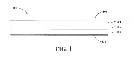
[0011] Figure 1 is a cross-sectional view of an ECB, according
to an embodiment of the present disclosure;
[0012] Figure 2 is an exploded view of different layers of the
ECB of Figure 1;
[0013] Figure 3 is an exploded view of different sheets of
materials for laminating as a bonding layer of the ECB in Figures 1
and 2;
[0014] Figure 4 is a cross-sectional view of an ECB according
to another embodiment of the present disclosure;
- 3 -
CA 03058455 2019-09-27
WO 2018/183787
PCT/US2018/025317
[0015] Figure 5 is a cross-sectional view of an ECB according
to another embodiment of the present disclosure;
[0016] Figure 6 is an exploded view of different layers of the
ECB of Figure 5;
[0017] Figure 7 is a cross-sectional view of an ECB according
to another embodiment of the present disclosure; and
[0018] Figure 8 is a flow chart illustrating a process of
constructing an ECB, according to an embodiment of the present
disclosure.
[0019] Similar reference numerals may have been used in
different figures to denote similar components.
DETAILED DE5.7271IrTION OF THE 7E77-.:FERRED EMBODIMENTS
[0020] Figure 1 illustrates an embodiment of an ECB generally
shown at 100. The ECB 100 includes a first conductive layer 102, a
first bonding layer 104, a heat insulating layer 106, a second
bonding layer 108, and a second conductive layer 110. As
illustrated in Figure 2, each of the layers 102, 104, 106, 108, and
110 has a first surface and a second surface. In the example of
Figure 2, the first surface is a top surface and the second surface is
a bottom surface. The top surface of the first bonding layer 104 is
configured to securely attach to the bottom surface of the first
conductive layer 102, the top surface of the heat insulating layer
106 is configured to securely attach to the bottom surface the first
bonding layer 104, the top surface of the second bonding layer 108
=25 is configured to securely attach to the bottom surface of the heat
insulating layer 106, and the top surface of the second conductive
layer 110 is configured to securely attach to the bottom surface of
the second bonding layer 108.
[0021] Each of the first and second conductive layers 102 and
110 conduct electricity between the electrical elements and circuits
- 4 -
CA 03058455 2019-09-27
WO 2018/183787
PCT/US2018/025317
mounted on the respective conductive layers of the ECB 100. The
first and second conductive layers 102 and 110 are made of
materials for conducting electricity. The conductive layers 102 and
110 may be made of metal. For example, the conductive layers
102 and 110 may be copper foils, such as InsulectroTM type H1.
[0022] The first and second bonding layers 104 and 108 and
the heat insulating layer 106 are interlayers between the
conductive layers 102 and 110. The term interlayer, or substrate
layer, refers to the one or more dielectric layers placed between
two conductive layers 102 and 110. An interlayer may include one
or more bonding layers, one or more heat insulating layers, or a
combination thereof. In the example of Figure 1, the first bonding
layer 104 bonds the first conductive layer 102 and the heat
insulating layer 106, and the second bonding layer 108 bonds the
heat insulating layer 106 and the second conductive layer 110.
[0023] As illustrated in Figure 3, a bonding layer 300, such as
each of the first and second bonding layers 104 and 108, is made
from a plurality of sheets of bonding materials 302. The bonding
layer 300 is made of bonding materials that can sustain a cure
temperature and pressure of a laminating process. For example,
the bonding layer 300 does not melt at the cure temperature.
Materials suitable for FR1 to FR4 composite materials may be used
as the bonding materials. For example, the bonding layer 300 may
be made of a plurality of sheets of fiberglass, pre-impregnated
with epoxy resin, also known as prepreg. The bonding layer 300
may be made of Insulectro-rm 106NF prepreg. In an example, the
bonding layer 300 is made of a plurality of sheets of InsulectroTM
106NF prepreg.
[0024] The heat insulating layer 106 includes thermal
barriers. The heat insulating layer 106 reduces heat transfer from
- 5 -
CA 03058455 2019-09-27
WO 2018/183787
PCT/US2018/025317
the electrical elements or circuits on a conductive layer to the
opposite conductive layer of an ECB, for example, from conductive
layer 102 to the conductive layer 110, or vice versa. The heat
insulating layer 106 may be made of any heat resistant material as
a thermal barrier. If the heat insulating layer 106 is laminated
with the other bonding layers 104 and 108, the heat resistant
materials of the heat insulating layer 106 must also withstand the
cure temperature and pressure required by the bonding layers 104
and 108 during the laminating process. The heat resistant
materials include, but are not limited to, natural fiber insulators,
cotton, and wool. The heat insulating layer 106 may be made of
Nomex woven fabric, tight weave. In an example, the heat
insulating layer 106 contains one sheet of 1-5 oz./yd2 Nomex
woven fabric, tight weave.
[0025] The layers 102, 104, 106, 108 and 110 may be
bonded together as the ECB 100 by a laminating process. In some
examples, the layers 102, 104, 106, 108 and 110 are stacked
together from the top to the bottom, aligned with each other as
illustrated in Figure 2, and placed on a heated press. Sufficient
pressure, such as 50 tons of pressure for an area of 18"x24", is
applied to the stack of layers 102, 104, 106, 108 and 110 to reach
a desired thickness of the ECB 100, such as 1.2mm. The
laminating process may be conducted under a vacuum condition
using a cure temperature that the bonding materials and the
insulating materials can withstand. In an example where the
bonding layers 104 and 108 are InsulectroTM 106 NF prepreg and
the heat insulating layer 106 is the Nomex woven fabric, tight
weave, the cure temperature is 360 F. Generally, a cure
temperature is recommended by the manufacturer of the relevant
materials used in the bonding layers 104 and 108 or in the heat
insulating layer 106. The cure temperature may be varied for other
types of bonding materials, such as other prepregs. The laminated
- 6 -
CA 03058455 2019-09-27
WO 2018/183787
PCT/US2018/025317
ECB 100 is cured for a period, for example, 70 minutes, as
recommended by the manufacturer of the relevant materials used
in the bonding layers 104 and 108 or in the heat insulating layer
106. In some examples, the entire laminating process is controlled
by a bonding press computer. The computer controls the process
of heating the stacked layers, the point at which to apply pressure,
and when to allow the stack to cool at a controlled rate.
[0026] By inclusion of the heat insulating layer 106 in the ECB
100 as a thermal barrier, the thermal conductivity of the ECB 100
is lower than typical FR4 ECB, and thus the heat insulating layer
106 reduces the thermal conductivity of the ECB 100 and may
improve the performance of heat sensitive electrical elements and
circuits mounted on one conductive layer of the ECB 100.
[0027] Figure 4 illustrates another embodiment of ECB 150.
As with the ECB 100, the ECB 150 includes a first conductive layer
102, a first bonding layer 104, a heat insulating layer 106, a
second bonding layer 108, and a second conductive layer 110. In
addition, in ECB 150, each of the first bonding layer 104, the heat
insulating layer 106, and the second bonding layer 108 contains a
plurality of air bubbles 112. In some examples, as illustrated in
Figure 4, the heat insulating layer 106 contains more air bubbles
than the bonding layers 104 and 108. In some examples, the air
bubbles 112 are microbubbles, the diameters of which may be in
an order of mm or pm.
[0028] The ECB 150 is made from the same laminating
process as the ECB 100 except that the stack of the layers 102,
104, 106, 108 and 110 are laminated under atmospheric pressure,
rather than under a vacuum condition. The laminating process
under atmospheric pressure generates air bubbles 112 in the
bonding layers 104 and 108 and in the heat insulating layer 106,
- 7 -
CA 03058455 2019-09-27
WO 2018/183787
PCT/US2018/025317
while the ECB 100 laminated under a vacuum condition is air
bubble free.
[0029] With the presence of air bubbles 112, the thermal
conductivity of the ECB 150 is further improved over ECB 100. Air
acts as a heat insulator, and the air bubbles 112 presented in the
bonding layers 104 and 108 and the heat insulating layer 106 in
ECB 150 serve as additional thermal barriers. As such, the ECB
150 has an improved heat insulating performance over the ECB
100.
[0030] In some examples, the heat insulating layer 106 in
ECB 150 may be omitted. In this case, the ECB 150 includes the
conductive layers 102 and 110, and at least one bonding layer 104
or 108. By laminating the layers 102, the at least one bonding
layer 104 and 108, and 110 under atmospheric pressure, air
bubbles 112 are generated in the at least one bonding layer 104
and 108 as thermal barriers. As such, the ECB 150 still has a
lower thermal conductivity than a typical FR4 ECB.
[0031] An ECB may include more than one insulating layer to
further reduce the thermal conductivity. In this regard, Figure 5
illustrates another embodiment of an ECB 200 that includes two
insulating layers. In the example of Figure 5, ECB 200 includes a
first conductive layer 202, a first bonding layer 204, a first heat
insulating layer 206, a second bonding layer 208, a second heat
insulating layer 210, a third bonding layer 212, and a second
conductive layer 214. In the example of Figure 5, the first bonding
layer 204 bonds the first conductive layer 202 and the first heat
insulating layer 206, the second bonding layer 208 bonds the first
heat insulating layer 206 and the second heat insulating layer 210
and the third bonding layer 212 bonds the second heat insulating
layer 210 and the second conductive layer 214.
-8 -
CA 03058455 2019-09-27
WO 2018/183787
PCT/US2018/025317
[0032] As illustrated in Figure 6, each of the layers 202, 204,
206, 208, 210, 212 and 214 has a first surface and a second
surface. In the example of Figure 6, the first surface is a top
surface and the second surface is a bottom surface. The top
surface of the first bonding layer 204 is configured to securely
attach to the bottom surface of the first conductive layer 202, the
top surface of the first heat insulating layer 206 is configured to
securely attach to the bottom surface the first bonding layer 204,
the top surface of the a second bonding layer 208 is configured to
securely attach to the bottom surface of the first heat insulating
layer 206, the top surface of the second heat insulating layer 210
is configured to securely attach to the bottom surface of the
second bonding layer 208, the top surface of the third bonding
layer 212 is configured to securely attach to the bottom surface of
the second heat insulating layer 210, and the top surface of the
second conductive layer 214 is configured to securely attach to the
bottom surface the third bonding layer 212.
[0033] The first and second conductive layers 202 and 214
are the same as the conductive layers 102 and 110 described
above. The first, second and third bonding layers 204, 208, and
212 are the same as the bonding layers 104 and 108 described
above. The first and second insulating layers 206 and 210 are the
same as the heat insulating layer 106 described above.
[0034] ECB 200 is different from ECB 100 in that ECB 200
includes one additional bonding layer and one additional insulation
layer between a conductive layer and a bonding layer. For
example, the first bonding layer 204 and the first heat insulating
layer 206 are added between the first conductive layer 202 and the
second bonding layer 208. Alternatively, ECB 200 includes one
additional insulating layer and one additional bonding layer
between a bonding layer and an insulating layer. For example, the
- 9 -
CA 03058455 2019-09-27
WO 2018/183787
PCT/US2018/025317
second bonding layer 208 and the second heat insulating layer 210
are added between the first insulating layer 206 and the third
bonding layer 212. An ECB may include two or more additional
bonding layers and insulation layers between a conductive layer
and a bonding layer of ECB 100, or between a bonding layer and
an insulating layer of ECB 100.
[0035] The bonding layers 204, 208, and 212 may include
various sheets of bonding materials. In an embodiment of the ECB
200, the first conductive layer 202 is an InsulectroTM type H1
copper foil; the first bonding layer 204 includes 5 sheets of
InsulectroTM 106NF prepreg; the first heat insulating layer 206
includes 1 sheet of 1-5 oz./yd2 Nomex woven fabric, tight weave;
the second bonding layer 208 includes 8 sheets of InsulectroTM
106NF prepreg; the second heat insulating layer 210 includes 1
sheet of 1-5 oz./yd2 Nomex woven fabric, tight weave; the third
bonding layer 212 includes 5 sheets of InsulectroTM 106NF prepreg;
and the second conductive layer 214 is an InsulectroTM type H1
copper foil.
[0036] In another embodiment of the ECB 200, the first
conductive layer 202 is an InsulectroTM type H1 copper foil; the
first bonding layer 204 includes 3 sheets of InsulectroTM 106NF
prepreg; the first heat insulating layer 206 includes 1 sheet of 1-5
oz./yd2 Nomex woven fabric, tight weave; the second bonding
layer 208 includes 12 sheets of InsulectroTM 106NF prepreg; the
second heat insulating layer 210 includes 1 sheet of 1-5 oz./yd2
Nomex woven fabric, tight weave; the third bonding layer 212
includes 3 sheets of InsulectroTM 106NF prepreg; and the second
conductive layer 214 is an InsulectroTM type H1 copper foil.
[0037] The layers 202, 204, 206, 208, 210, 212 and 214 may
be bonded together as an ECB 200 by a laminating process. In
- 10 -
CA 03058455 2019-09-27
WO 2018/183787
PCT/US2018/025317
some examples, the layers 202, 204, 206, 208, 210, 212 and 214
are stacked from the top to the bottom as described above and as
shown in Figure 6, and placed on a heated press. The same
laminating process described above under a vacuum condition with
respect to the ECB 100 is applied to the stacked layers. By
introducing the insulating layers 206 and 210 into the ECB 200 as
thermal barriers, the thermal conductivity of the ECB 200 is lower
than a typical FR4 ECB. Therefore, the insulating layers 206 and
210 may improve the performance of heat sensitive electrical
elements and circuits mounted on the ECB 200. As well, thermal
conductivity may be further reduced in ECB 200 over ECB 100
since one additional heat insulating layer or thermal barrier is used
in ECB 200.
[0038] Figure 7 illustrates another embodiment of an ECB
250. As with the ECB 200, the ECB 250 includes a first conductive
layer 202, a first bonding layer 204, a first heat insulating layer
206, a second bonding layer 208, a second heat insulating layer
210, a third bonding layer 212, and a second conductive layer 214.
In addition, in ECB 250, each of the first bonding layer 204, the
first heat insulating layer 206, the second bonding layer 208, the
second heat insulating layer 210, and the third bonding layer 212
contains a plurality of air bubbles 216. In some examples, as
illustrated in Figure 7, each of the insulating layers 206 and 210
contains more air bubbles than each of the bonding layers 204,
208 and 212. In some examples, the air bubbles 216 are
microbubbles, the diameters of which may be in an order of mm or
pm.
[0039] The layers 202, 204, 206, 208, 210, 212 and 214 may
be bonded together as the ECB 250 from the same laminating
process described above with respect to the ECB 200 except that
the stack of layers 202, 204, 206, 208, 210, 212 and 214 are
-11 -
CA 03058455 2019-09-27
WO 2018/183787
PCT/US2018/025317
laminated under atmospheric pressure, rather than under a
vacuum condition. The laminating process under atmospheric
pressure generates air bubbles 216 in the bonding layers 204, 208
and 212, and in the insulating layers 206 and 210, while the ECB
200 laminated under a vacuum condition is air bubble free.
[0040] With the air bubbles 216, the thermal conductivity of
the ECB 250 is further improved over ECB 200. The air bubbles
216 in each of the insulating layers 206 and 210 and the bonding
layers 204, 208 and 212 in ECB 250 serve as additional thermal
barriers. As such, the ECB 250 has an improved heat insulating
performance over ECB 200. In some examples, the ECB 250
achieves a thermal conductivity value of 0.09-0.2 W/mK.
[0041] In some examples, the insulating layers 206 and 210
in ECB 250 may be omitted. In this case, the ECB 250 includes
the conductive layers 202 and 214, and at least one bonding layer
204, 208 or 212. By laminating the layers 202, at least one
bonding layer 204, 208 and 212, and 214 under atmospheric
pressure, air bubbles 216 are generated in the at least one
bonding layer 204, 208 and 212 as thermal barriers. As such, the
ECB 250 still has a lower thermal conductivity than a typical FR4
ECB.
[0042] As well, the ECB 200 or 250 exhibits mechanical
properties permitting it to be easily machined, maintains sufficient
mechanical resistance to thermal shocks, and offers satisfactory
thermal isolation from one conductive layer of the ECB 200 or 250
to the opposite conductive layer.
[0043] Typically, the thermal conductivity value of the ECB
varies inversely with the number of bonding layers and the number
- 12-
CA 03058455 2019-09-27
WO 2018/183787
PCT/US2018/025317
of insulating layers that are included in the ECB. The ECB may be
thicker than the embodiments described above. For example, the
ECB 100, 150, 200 or 250 may include more insulating layers and
bonding layers, resulting in an ECB with a thickness of 2.5 mm
with a lower thermal connectivity value, for example, 0.05-0.2
W/mK. The number of sheets of the material forming the bonding
layer 104, 108, 204, 208 or 212 may be varied, as long as the
bonding layer securely attaches to the heat insulating layer 106,
206 or 210 and/or to the conductive layer 102, 110, 202 or 214. If
the number of the sheets of bonding materials used in forming a
bonding layer increases, the mechanical strength of the ECB may
be improved.
[0044] Embodiments of ECB 100, 150, 200 and 250 can be
used on various electrical applications, for example, on a cooling or
heating circuit of a vehicle seat.
[0045] Alternatively, embodiments of ECB 100, 150, 200 and
250 can be used in conjunction with flexible printed circuits on
which conductive traces are bonded on a flexible dielectric
substrate. For example, a flexible printed circuit may be securely
attached to a side of the ECB 100, 150, 200 and 250, and the
conductive traces of the flexible printed circuit may form a
conductive layer of ECB 100, 150, 200, and 250. In these electrical
applications, ECB 100, 150, 200 and 250 may be constructed with
two, one, or zero conductive layers 102, 110, 202 or 214. When
used with flexible printed circuits, ECB 100, 150, 200 and 250 can
serve the purpose of locally rigidizing a flexible circuit in a given
area while thermally isolating each side of the ECB. ECB 100, 150,
200 and 250 constructed with two, one, or zero conductive layers
102, 110, 202 or 214 can also be used on a cooling or heating
circuit of a vehicle seat.
- 13-
CA 03058455 2019-09-27
WO 2018/183787
PCT/US2018/025317
[0046] Figure 8 illustrates an exemplary process for
constructing an ECB. At least one interlayer, such as layer 104,
106, or 108 in the examples of Figures 1-2 and 4, or layer 204,
206, 208, 210, or 212 in the examples of Figures 5-7, is selected
and stacked between the two conductive layers on a heated press,
such as layer 102 and 110 or layers 202 and 214 in Figures 5-7
(step 802). The interlayer may include at least one sheet of
relevant materials, such as bonding materials or heat insulating
materials as described above. The conductive layers and the at
least one interlayer are arranged in an order so that both surfaces
of the at least one interlayer are bonded with a respective
conductive layer. For example, the layers are placed in a heated
press in an order as described in the laminating processes for ECB
100, ECB 150, ECB 200, and ECB 250.
[0047] The stacked layers are then bonded to construct an
ECB, such as ECB 100, ECB 150, ECB 200, or ECB 250, by applying
a laminating process (step 804). For example, as described above
in the laminating processes for ECB 100, ECB 150, ECB 200, and
ECB 250, at a cure temperature that the bonding layer and or the
heat insulating layer can withstand without melting, sufficient
pressure is applied to the loose stacked layers until a desired
thickness of the ECB is reached, such as 0.6 mm-2.5mm.
[0048] In some examples, the interlayer includes at least one
of a heat insulating layer and a bonding layer, and the laminating
process is conducted on the stacked layers under a vacuum
condition. In this case, no air bubbles are generated in the
interlayer, as described in the laminating process of ECB 100 and
200.
- 14
CA 03058455 2019-09-27
WO 2018/183787
PCT/US2018/025317
[0049] In some examples, the interlayer includes at least one
of a heat insulating layer and a bonding layer, and the laminating
process is conducted on the stacked layers under an atmospheric
pressure. In this case, air bubbles, such as air bubbles 112 in ECB
150 or air bubbles 216 in ECB 250, are generated in the interlayer
as an additional thermal barrier, for example, as described in the
laminating process of ECB 150 and 250.
[0050] The laminated ECB is cured for a period (step 806), for
example, 70 minutes. The cure period of the ECB varies based on
the interlayer materials used and generally is recommended by the
manufacturer of the interlayer materials. The cured ECB may be
further polished.
[0051] The invention has been described in an illustrative
manner, and it is to be understood that the terminology which has
been used is intended to be in the nature of words of description
rather than of limitation. Many modifications and variations of the
present invention are possible in light of the above teachings. It is,
therefore, to be understood that within the scope of the appended
claims, the invention may be practiced other than as specifically
described.
- 15-