Note: Descriptions are shown in the official language in which they were submitted.
RF CIRCULATOR
TECHNICAL FIELD OF THE INVENTION
The present invention relates in general to the field of RF circulators, and
more particularly, to a
novel optimized high frequency RF circulator.
BACKGROUND OF THE INVENTION
Without limiting the scope of the invention, its background is described in
connection with RF
circulators.
United States Patent No. 9,250,452, issued to Yap, et al., entitled ``Tunable
photonic RF circulator
for simultaneous transmit and receive", is said to teach a photonic RF
circulator that provides
greater than 40 db of isolation between a Received RF signal and a Transmitted
RF signal in a
simultaneous transmit and receive device. The photonic RF circulator is said
to use light
modulation in an optical waveguide grating where the Received RF signal co-
propagates with the
light and the Transmitted RF signal counter-propagates with the light. In
addition, it is said to
describe variations that provide for broadening the bandwidth of the T/R
isolation and rejection of
various noise sources.
United States Patent No. 7,362,195, issued to Chui, entitled -Ferro magnetic
metal-insulator
multilayer radio frequency circulator", is said to teach a directional RF
circulator that directs radio
frequency signals without an external biasing magnetic field. The directional
RF circulator
includes layers of ferromagnetic materials and insulating materials that form
a laminated nano-
structure. The layers of ferromagnetic materials and insulating materials are
selected to have a
thickness smaller than the wavelength of the radio frequency signals, and
smaller than the skin
depth of the signals in the material. The ferromagnetic materials and
insulators form a resonant
cavity having a resonant frequency near the operating frequency for the
signal, and a plurality of
connectors can be located around the periphery of the laminated ferromagnetic
material to provide
input and output ports for the device. This RF circulator is also said to be
compatible with
semiconductor thin-film processing, and may be integrated onto a monolithic
integrated circuit. A
method of forming a directional RF circulator is also said to be disclosed.
SUMMARY OF THE INVENTION
The circulator/isolator devices of the present invention can be used for
devices and arrays in glass
ceramic substrates for electronic, microwave and radiofrequency in general. In
one embodiment,
the present invention includes a circulator/isolator device comprising: a
substrate comprising one or
more conductive coils, wherein the substrate is a photosensitive glass ceramic
composite substrate
1
Date Recue/Date Received 2021-03-12
comprising at least silica, lithium oxide, aluminum oxide, and cerium oxide,
and wherein the one
or more conductive coils are formed in, on, or about the substrate; an opening
in the substrate
comprising an iron core, wherein the iron core is formed in the substrate
after the formation of the
one or more conductive coils, wherein the iron core is positioned and shaped
to create a
circulator/isolator in the substrate; and one or more connectors, vias,
resistors, capacitors, or other
integrated circuits of devices connected to the circulator/isolator. In one
aspect, the device further
comprises a passivation or coating on the device to protect the device from
the environment. In
another aspect, the iron core is formed in situ after formation of the one or
more conductive coils.
In another aspect, the conductive coils comprise copper. In another aspect,
the circulator/isolator
device has a reduced signal loss when compared to existing circulator/isolator
devices. In another
aspect, the circulator/isolator device has a loss of less than 50, 40, 30, 25,
20, 15, or 10% of the
signal input versus a signal output. In another aspect, the iron core
comprises melted or sintered
iron particles, microparticles, or nanoparticles.
In another aspect, geometry of the
circulator/isolator device is substantially circular. In another aspect, the
substrate is glass. In
another aspect, the substrate is a glass substrate comprising a composition
of: 60 - 76 weight %
silica; at least 3 weight % K20 with 6 weight % - 16 weight % of a combination
of K20 and Na2O;
0.003-1 weight % of at least one oxide selected from the group consisting of
Ag2O and Au20;
0.003-2 weight % Cu2O; 0.75 weight % - 7 weight % B203, and 6 - 7 weight %
Al2O3; with the
combination of B203; and Al2O3 not exceeding 13 weight %; 8-15 weight % Li2O;
and 0.001 ¨ 0.1
weight % Ce02. In another aspect, the substrate is a glass substrate
comprising a composition of:
35 - 76 weight % silica, 3- 16 weight % K20, 0.003-1 weight % Ag2O, 0.75-13
weight % B203, 8-
15 weight % Li2O, and 0.001 ¨ 0.1 weight % Ce02. In another aspect, the the
substrate is at least
one of: a photo-definable glass substrate comprises at least 0.3 weight %
Sb203 or As203; a photo-
definable glass substrate comprises 0.003-1 weight % Au20; a photo-definable
glass substrate
comprises 1-18 weight % of an oxide selected from the group consisting of CaO,
ZnO, Pb0, MgO
and BaO; and optionally has an anisotropic-etch ratio of exposed portion to
said unexposed portion
is at least one of 10-20:1; 21-29:1; 30-45:1; 20-40:1; 41-45:1; and 30-50:1.
In another aspect, the
substrate is a photosensitive glass ceramic composite substrate comprising at
least silica, lithium
oxide, aluminum oxide, and cerium oxide.
In another embodiment, the present invention also includes a method for making
a
circulator/isolator device, the method comprising: forming on a substrate one
or more conductive
coils, wherein the substrate is a photosensitive glass ceramic composite
substrate comprising at
least silica, lithium oxide, aluminum oxide, and cerium oxide, and wherein the
one or more
conductive coils are formed in, on, or about the substrate; etching an opening
in the substrate;
depositing iron particles in the opening; melting or sintering the iron
particles into an iron core,
2
Date Recue/Date Received 2021-03-12
wherein the iron core is formed in the substrate after the formation of the
one or more conductive
coils, wherein the iron core is positioned and shaped to create a
circulator/isolator in the substrate;
and connecting the conductive coils of the circulator/isolator to one or more
connectors, vias,
resistors, capacitors, or other integrated circuits of devices connected to
the circulator/isolator
device. In one aspect, the method further comprises coating or depositing a
passivation or coating
on the circulator/isolator device to protect the circulator/isolator device
from the environment. In
another aspect, the method further comprises forming iron core in situ after
the step of forming the
one or more conductive coils. In another aspect, the method further comprises
forming iron core in
situ after the step of forming the one or more conductive coils in the
presence of a noble gas. In
another aspect, the conductive coils comprise copper. In another aspect, the
circulator/isolator
device has a reduced signal loss when compared to existing circulator/isolator
devices. In another
aspect, the circulator/isolator device has a loss of less than 50, 40, 30, 25,
20, 15, or 10% of the
signal input versus an signal output. In another aspect, the iron core
comprises melted or sintered
iron particles, microparticles, or nanoparticles.
In another aspect, a geometry of the
circulator/isolator device is substantially circular. In another aspect, the
substrate is a glass
substrate comprising a composition of: 60 - 76 weight % silica; at least 3
weight % K20 with 6
weight % - 16 weight % of a combination of K20 and Na2O; 0.003-1 weight % of
at least one
oxide selected from the group consisting of Ag2O and Au20; 0.003-2 weight %
Cu2O; 0.75 weight
% - 7 weight % B203, and 6 - 7 weight % Al2O3; with the combination of B203;
and Al2O3 not
exceeding 13 weight %; 8-15 weight % Li2O; and 0.001 ¨ 0.1 weight % Ce02. In
another aspect,
the substrate is a glass substrate comprising a composition of: 35 - 76 weight
% silica, 3- 16 weight
% K20, 0.003-1 weight % Ag2O, 0.75-13 weight % B203, 8-15 weight % Li2O, and
0.001 ¨ 0.1
weight % Ce02. In another aspect, the substrate is at least one of: a photo-
definable glass substrate
comprises at least 0.3 weight % Sb203 or As203; a photo-definable glass
substrate comprises 0.003-
1 weight % Au20; a photo-definable glass substrate comprises 1-18 weight % of
an oxide selected
from the group consisting of CaO, ZnO, Pb0, MgO and BaO; and optionally has an
anisotropic-
etch ratio of exposed portion to said unexposed portion is at least one of 10-
20:1; 21-29:1; 30-45:1;
20-40:1; 41-45:1; and 30-50:1. In another aspect, the substrate is a
photosensitive glass ceramic
composite substrate comprising at least silica, lithium oxide, aluminum oxide,
and cerium oxide.
In another embodiment, an RF circulator/isolator device is made by a method
comprising: forming
on a substrate one or more conductive coils, wherein the substrate is a
photosensitive glass ceramic
composite substrate comprising at least silica, lithium oxide, aluminum oxide,
and cerium oxide,
and wherein the one or more conductive coils are formed in, on, or about the
substrate; etching an
opening in the substrate; depositing iron particles in the opening; melting or
sintering the iron
particles into an iron core, wherein the iron core is formed in the substrate
after the formation of the
3
Date Recue/Date Received 2021-03-12
one or more conductive coils, wherein the iron core is positioned and shaped
to create a
circulator/isolator in the substrate; and connecting the conductive coils of
the circulator/isolator to,
e.g., an amplifier, an antenna, a resistor, a capacitor, etc.
BRIEF DESCRIPTION OF THE DRAWINGS
For a more complete understanding of the features and advantages of the
present invention,
reference is now made to the detailed description of the invention along with
the accompanying
figures and in which:
FIG. 1 shows an RF circulator/isolator devices of the present invention.
FIG. 2 shows the results from the RF circulator/isolator device of the present
invention.
DETAILED DESCRIPTION OF THE INVENTION
While the making and using of various embodiments of the present invention are
discussed in
detail below, it should be appreciated that the present invention provides
many applicable inventive
concepts that can be embodied in a wide variety of specific contexts. The
specific embodiments
discussed herein are merely illustrative of specific ways to make and use the
invention and do not
delimit the scope of the invention.
To facilitate the understanding of this invention, a number of terms are
defined below. Terms
defined herein have meanings as commonly understood by a person of ordinary
skill in the areas
relevant to the present invention. Terms such as "a-, "an- and "the- are not
intended to refer to
only a singular entity, but include the general class of which a specific
example may be used for
illustration. The terminology herein is used to describe specific embodiments
of the invention, but
their usage does not limit the invention, except as outlined in the claims.
The circulator/isolator devices of the present invention can be used for
devices and arrays in glass
ceramic substrates for electronic, microwave and radiofrequency in general.
This invention
provides creates a cost effective glass ceramic inductive individual or array
device. Where glass
ceramic substrate has demonstrated capability to form such structures through
the processing of
both the vertical as well as horizontal planes either separately or at the
same time to form
circulator/isolator devices that can be used in a wide variety of
telecommunications and other
platforms. The novel circulator/isolator glass ceramic devices can be made as
stand-alone devices
to add to other devices, can be built into a substrate directly and then
connected to other electronic
components using vias, wire or ball bonding, etc.
In one embodiment, the present invention is a RF circulator/isolator built for
an integrated passive
device (IPD) that has a decreased size versus currently available options. The
present invention
4
Date Recue/Date Received 2021-03-12
can be made by optimizating an Iron Core Material in a Test Vehicle. The test
vehicle can include,
e.g., one or more types of glass made and formulated as described hereinbelow
obtained from, e.g.,
3DGS, USA, with methods and parts for improved by iron core filling. First, a
standard cavity
depth will be used to ensure consistent measurement. Next, components that are
formed, added or
connected to form a circuit are connected to the circulator/isolator and are
then evaluated as testing
proceeds and specific volumes are necessary for accurate calculations.
FIG. 1 shows an RF circulator/isolator devices of the present invention. The
present invention
includes a method of fabrication a RF circulator/isolator device made by
preparing a photosensitive
glass ceramic composite substrate comprising at least silica, lithium oxide,
aluminum oxide, and
cerium oxide, masking a design layout comprising one or more, two or three
dimensional inductive
device in the photosensitive glass substrate, exposing at least one portion of
the photosensitive
glass substrate to an activating energy source, exposing the photosensitive
glass substrate to a
heating phase of at least ten minutes above its glass transition temperature,
cooling the
photosensitive glass substrate to transform at least part of the exposed glass
to a crystalline material
to form a glass-crystalline substrate and etching the glass-crystalline
substrate with an etchant
solution to form one or more angled channels or through holes that are then
used in the RF
circulator/isolator.
The RF circulator/isolator can be built in, on, our about a glass ceramic
(APEX O Glass ceramiem,
3DGS, USA) as a novel packaging and substrate material for semiconductors, RF
electronics,
microwave electronics, and optical imaging. APEX Glass ceramic is processed
using first
generation semiconductor equipment in a simple three step process and the
final material can be
fashioned into either glass, ceramic, or contain regions of both glass and
ceramic. The APEX
Glass ceramic possesses several benefits over current materials, including:
easily fabricated high
density vias, demonstrated microfluidic capability, micro-lens or micro-lens
array, high Young's
modulus for stiffer packages, halogen free manufacturing, and economical
manufacturing.
Photoetchable glasses have several advantages for the fabrication of a wide
variety of
microsystems components. Microstructures have been produced relatively
inexpensively with these
glasses using conventional semiconductor processing equipment. In general,
glasses have high
temperature stability, good mechanical and electrically properties, and have
better chemical
.. resistance than plastics and many metals. One example of a glass ceramic
for making the RF
circulator/isolator of the present invention includes, for example, silicon
oxide (5i02) of 75-85% by
weight, lithium oxide (Li2O) of 7-11% by weight, aluminum oxide (A1203) of 3-
6% by weight,
sodium oxide (Na2O) of 1-2% by weight, 0.2-0.5% by weight antimonium trioxide
(513203) or
arsenic oxide (As203), silver oxide (Ag2O) of 0.05-0.15% by weight, and cerium
oxide (Ce02)
of 0.01- 0.04% by weight As used herein the terms "APEX R Glass ceramic",
"APEX R glass" or
5
Date Recue/Date Received 2021-03-12
simply -APEX" are used to denote one embodiment of the glass ceramic
composition for
making the RF circulator/isolator of the present invention.
The APEXTM glass can be filled with metal, alloys, composites, glass or other
magnetic media, by
a number of methods including plating or vapor phase deposition. The magnetic
permittivity of the
media combined with the dimensions and number of structures (loops, turns or
other inductive
element) in the device provide the inductance of devices. Depending on the
frequency of operation
the RF circulator/isolator device design will require different magnetic
permittivity materials. At
low frequencies, less than 100 MHz devices can use ferrites or other high
different magnetic
permittivity materials. At higher frequencies >100MHz high different magnetic
permittivity
.. materials can generate eddy currents creating large electrical losses. So
at higher frequency
operations material such as copper or other similar material is the media of
choice for RF
circulator/isolator devices. Once the RF circulator/isolator device has been
generated the
supporting APEX:TM glass can be left in place or removed to create a free-
standing structure such
as the RF circulator/isolator of the present invention.
To avoid the problems with making devices in glass ceramics, the present
invention uses glass
ceramics with an average etch aspect ratio greater than 50:1. This allows
users to create smaller
and deeper features. Additionally, the manufacturing process taught herein
enables product
yields of greater than 90% (legacy glass yields are closer to 50%). Lastly, in
legacy glass
ceramics, approximately only 30% of the glass is converted into the ceramic
state, whereas
with APEXTM Glass ceramic this conversion is closer to 70%.
The present invention includes a method for fabricating a RF
circulator/isolator in a glass ceramic
structure for use in forming RF circulator/isolator structures used in
electromagnetic transmission,
transformers, filtering and other applications.
The present invention includes an RF
circulator/isolator structure created in the multiple planes of a glass-
ceramic substrate, such process
employing the (a) exposure to excitation energy such that the exposure occurs
at various angles by
either altering the orientation of the substrate or of the energy source, (b)
a bake step and (c) an
etch step. Angle sizes can be either acute or obtuse. The curved and digital
structures are difficult,
if not infeasible to create in most glass, ceramic or silicon substrates. The
present invention has
created the capability to create such RF circulator/isolator structures in
both the vertical as well as
horizontal plane for glass-ceramic substrates. The present invention includes
a method for
fabricating of a RF circulator/isolator structure on or in a glass ceramic.
Ceramicization of the glass is accomplished by exposing the entire glass
substrate to approximately
20J/cm2 of 310nm light. When trying to create glass spaces within the ceramic,
users expose all
of the material, except where the glass is to remain glass. In one embodiment,
the present
6
Date Recue/Date Received 2021-03-12
invention can use, e.g., a quartz/chrome mask containing the various
components of the RF
circulator/isolator, e.g., the coil(s), connectors or electrical conductor(s),
capacitor(s), resistor(s),
ferrous and/or ferromagnetic component(s), etc.
The present invention includes a method for fabricating a RF
circulator/isolator device in or on
glass ceramic structure electrical microwave and radio frequency applications.
The glass ceramic
substrate may be a photosensitive glass substrate having a wide number of
compositional variations
including but not limited to: 60 - 76 weight % silica; at least 3 weight % K20
with 6 weight % - 16
weight % of a combination of K20 and Na2O; 0.003-1 weight % of at least one
oxide selected from
the group consisting of Ag2O and Au20; 0.003-2 weight % Cu2O; 0.75 weight % -
7 weight %
B203, and 6 - 7 weight % Al2O3; with the combination of B203; and A1203 not
exceeding 13 weight
%; 8-15 weight % Li2O; and 0.001 ¨ 0.1 weight % Ce02. This and other varied
compositions are
generally referred to as the APEXTM glass.
Any exposed portion may be transformed into a crystalline material by heating
the glass substrate
to a temperature near the glass transformation temperature. When etching the
glass substrate in an
etchant such as hydrofluoric acid, the anisotropic-etch ratio of the exposed
portion to the
unexposed portion is at least 30:1 when the glass is exposed to a broad
spectrum mid-ultraviolet
(about 308-312 nm) flood lamp to provide a shaped glass structure that have an
aspect ratio of at
least 30:1, and to create an inductive structure. The mask for the exposure
can be of a halftone
mask that provides a continuous grey scale to the exposure to form a curved
structure for the
.. creation of an inductive structure/device. A digital mask can also be used
with the flood exposure
and can be used to produce for the creation an inductive structure/device. The
exposed glass is
then baked typically in a two-step process. Temperature range heated between
of 420 C-520 C for
between 10 minutes to 2 hours, for the coalescing of silver ions into silver
nanoparticles and
temperature range heated between 520 C-620 C for between 10 minutes and 2
hours allowing the
lithium oxide to form around the silver nanoparticles. The glass plate is then
etched. The glass
substrate is etched in an etchant, of HF solution, typically 5% to 10% by
volume, wherein the etch
ratio of exposed portion to that of the unexposed portion is at least 30:1
when exposed with a broad
spectrum mid-ultraviolet flood light, and greater than 30:1 when exposed with
a laser, to provide a
shaped glass structure with an anisotropic-etch ratio of at least 30:1. In
certain cases, the material
surrounding the RF circulator/isolator device is converted to ceramic before
metal filling to make
the RF circulator/isolator of the present invention.
Some of the optimization parameters include, but are not limited to: (1)
independent variables to be
manipulated will be: a) iron content b) epoxy content c) bake time d) bake
temp e) type of iron 0
cavity height g) vacuum pulling to degas iron core; (2) optimization of the
iron core material will
7
Date Recue/Date Received 2021-03-12
be achieved when an iron ratio is determined that maintains structural
integrity and original
electrical parameters through reliability testing; and/or (3) identification
of an ideal material that
can be used consistently from one part to the next and follows or uses a
standardized set of
parameters that can be used by the customer for specific customer part
optimization.
Next, one or more validation Steps can be followed, including, but not limited
to: (1) Visual
inspection will include a measurement of cavity depth before filling with iron
and a recess
measurement performed after iron fill. Quality of iron dispersion throughout
hybrid material will be
inspected; (2) Conductance will be measured prior to iron fill, after iron
fill and again after
reliability testing; (3) Reliability will be primarily measured with a set
number of thermocycler
rotations. Visual inspection and conductance will be performed an additional
time after
thermocyling. If necessary, parts will be pulled from the thermocycler,
tested, and then placed back
into the thermocycler for a greater number of cycles to create a time study
for the amount of
temperature cycling a part can withstand while maintaining consistent
parameters; and/or (4)
Inductance measurements will be performed before iron fill and then will also
be taken before and
after reliability to determine the overall improvement of adding the iron core
and then the
consistency of the iron core over time and with temperature cycling.
Moreover, the Iron Hybrid Material can also be optimized or identified. To do
so, one or more
core measurements are obtained or determined. Non-limiting examples of core
measurements can
include: (1) a quantifiable value or range of values for magnetic and
electrical character of the iron
hybrid material. (2) temperature ranges and a timeframe that the material can
be expected to
withstand for the selected ratio of iron present in the final hybrid material.
(3) The material can be
evaluated using thermocycler testing at given number of cycle and repeating.
(4) In addition, the
zeta, stereoscope and other microscopes will be used to analyze surface grain,
recess and
qualitative assessment for iron hybrid dispersion and packing. (5)
Permittivity values will be
theoretically achieved using conductance (representing imaginary values) and
capacitative vs.
inductive effect (representing real values). The ratio of real and imaginary
(if determined to be a
finite value) will then be used to provide a value for the phase lag between
electrical and magnetic
properties in the material.
As regards the Permittivity values, these can include using: (1) a cavity
resonator (aka RF
resonator) can be used to calculate the permittivity in an experimental
setting. Define: Cavity
resonator = a sealed container that can run electromagnetic waves back and
forth across the cavity.
It will be interrupted by the iron hybrid substrate which can be compared to a
calibrated standard
for the empty container. (2) The development and use of a separate toroidal
inductor (manually
wound wire) could also yield potential for measurement of inductance for
permittivity calculations.
8
Date Recue/Date Received 2021-03-12
(3) Drafting of a code to assess further parameters of relative permittivity
(dielectric constant) as
well as complex permittivity (interaction of electric and magnetic waves).
As regards permeability of the iron hybrid, this can be determined by
implementing the particle
size of the iron and an evaluation of grain structure and this will lead to
more information on the
magnetization of the iron as well as the magnetic field itself. The
measurements can also include
scanning electron microscopy (SEM)/ Energy Dispersive X-Ray (EDX) to determine
the
arrangement and spacing between iron aggregated particles. Zeta images can be
used to evaluate
grain structure patterns present on the surface of the material. This can also
be used to assess
differences between different iron materials because grain structure will
vary. Further, resistance
measurements can be measured on Rohde & Schwarz as well as existing using
existing toolsets and
can be translated into the current present in the inductor. The absolute
permeability can be
determined with the inductor resistance, frequency, and/or input voltage.
Additionally, absolute can
be compared to theoretical using the number of turns on the given inductor.
As regards Frequency values, these can also be measured along with
permeability to determine
how the permeability will affect the frequency at which the customer component
should be
evaluated. This will help to further define the appropriate ratio in the iron
hybrid material.
Furthermore, this will define ranges that are real or complex and will aid in
the determination of
loss tangent. For example, a Rohde & Schwarz toolset as well as other
available tools can be used
to measure frequency values for individual parts. This falls in line with the
existing techniques used
to evaluate for frequency. Thus, overall knowledge of iron hybrid material
will lead into next steps
to determine how to apply power to circulator and result in correct direction
of flow and the correct
cancellation of signals to avoid part damage or malfunction. Also,
Permittivity is a very important
value in this determination because it must be correctly polarized to run in
the correct direction.
The RF circulator/isolator can also be evaluated using a model Circulator in
Software. Software
sourcing can include: (1) NI AWR +Analyst (National Instruments, USA), which
has a custom
material section which includes areas to input permeability and complex
permittivity, and also
includes the opportunity to define permanent magnetics. First order software
can be used for EM
simulation. (2) COMSOL software (or similar physics-based simulation software
such as EMPro).
COMSOL, with the AC/DC module, is capable of adding in permanent magnets into
the simulation
environment. Additionally, the software is flexible to include custom
equations for the definition
that would be derived to define the magnetic core material. Several device
architectures and
product splits can also be modeled and transferred into 2D flat models with
defined layer
definitions for production. Finally, product build specifications (e.g.
substrate thickness, metal line
widths, etc.) and tolerances are determined.
9
Date Recue/Date Received 2021-03-12
Production of devices. Upon the completion of EM modeling, the design is
transferred from the
2D flat models into production lithography masks, which are then used to make
wafers with the RF
circulator/isolator in glass or ceramic.
Test and validation of the RF circulator/isolator. The product design will
incorporate both SMT
and probe-launched circulator structures. The RF circulator/isolator can be
made with surface
mount technologies (SMT) devices that can be soldered directly onto a printed
circuit board (PCB),
or something similar, test board that will be capable of 3-port testing of the
RF performance of the
circulator and de-embedding the connectors and test boards to validate the de-
embedded
performance of the circulator. The present inventors have developed a set of
low-loss SMT
launches and board-level calibration standards which will be leveraged for
this portion of the work.
A probe-launch circulator device with probe launch design and on-wafer
calibration structures can
be validated as low-loss test and calibration structures from 0.5 - 40GHz. For
example, a 250um
pitch ground-signal-ground (GSG) probes enable on wafer 3-port measurement of
the circulator as
an integrated passive device, which is designed and laid out as described
herein.
Product wafers can also include a variety of statistical process control (SPC)
monitors die (5
locations per wafer) for on-wafer production control. This includes the
following: (1) Standard
SPC monitoring, e.g., via resistance, surface metal line resistance
monitoring, layer-to-layer
alignment validation, and/or feature size validation. Also, standard RF SPC
monitoring can
include, inductor validation, capacitor validation, microstrip transmission
line performance
validation. Finally, advanced RF SPC monitoring for this product definition
can include: magnetic
core validation structure to ensure consistent magnetic core performance
and/or permanent magnet
validation structure to validate performance and alignment.
One non-limiting example of a substrate for use with the circulator/isolator
device present
invention includes, e.g., a glass micromachined with etch ratios of 30:1 or
more using a mid-
.. ultraviolet flood exposure system and potentially 40:1 or more (preferably
50:1 or more) using a
laser-based exposure system, to produce high-precision structures. Thus, for
example, with nearly
vertical wall slopes on both the inside and outside diameters of hollow
photostructured
microneedles only minor wall-thickness variation from tip to base would occur.
In addition,
microposts, which are non-hollow microneedles, may be micromachined to possess
a low wall
slope, enabling a decrease in the overall micropost diameter. Likewise, micro-
lenses can be shaped
with precisely controlled horizontal variations and have only minor vertical
variation.
Furthermore, the precision shape of a glass structure with an anisotropic-etch
ratio of 40:1 or more
can be used to determine the shape of a non-glass material in the negative
mold. A mold material
can be: (1) deposited onto a shaped glass structure with a high-anisotropic-
etch ratio to provide a
Date Recue/Date Received 2021-03-12
negative mold; (2) the negative mold removed from the glass device; (3) a non-
glass material cast
into the negative mold; (4) the material in the negative mold is solidified;
(5) the solidified non-
glass material removed from the negative mold to provide a precision (e.g.
anisotropic-etch ratio of
40:1 to 50:1) casting of a non-glass material. Furthermore, unlike expensive
dry-etching processes
used in silicon-semiconductor-type processes, this process can produce very
high anisotropic-etch
ratios with relatively inexpensive wet etching.
The circulator/isolator device of the present invention can be fabricated in a
shaped glass structure
with a high-anisotropic-etch ratio, using a photosensitive glass substrate
having a composition of:
60 - 76 weight % silica; at least 3 weight % K20 with 6 weight % - 16 weight %
of a combination
of K20 and Na2O; 0.003-1 weight % of at least one oxide selected from the
group consisting of
Ag2O and Au20; 0.003-2 weight % Cu2O; 0.75 weight % - 7 weight %B203, and 6 -
7 weight %
Al2O3; with the combination of B203; and Al2O3 not exceeding 13 weight %; 8-15
weight % Li2O;
and 0.001 ¨ 0.1 weight % Ce02. This varied composition is generally referred
to as the APEX. At
least one portion of the photosensitive glass substrate is exposed to
ultraviolet light, while leaving
.. at least a second portion of said glass substrate unexposed; the glass
substrate is heated to a
temperature near the glass transformation temperature to transform at least
part of the exposed
glass to a crystalline material; and the glass substrate is etched in an
etchant, wherein the etch ratio
of exposed portion to that of the unexposed portion is at least 30:1 when
exposed with a broad
spectrum mid-ultraviolet flood light, and greater than 30:1 when exposed with
a laser , to provide a
shaped glass structure with an anisotropic-etch ratio of at least 30:1.
Percentages herein are in
weight percent of the constituents.
The circulator/isolator device of the present invention can be fabricated in a
photosensitive, shaped
glass structure with a high-anisotropic-etch ratio, can be composed of: 35 -
76 weight % silica, 3-
16 weight % K20, 0.003-1 weight % Ag2O, 0.75-13 weight % B203, 8-15 weight %
Li2O, and
0.001 ¨ 0.1 weight % Ce02. This photosensitive glass is processed using at
least on of the
following steps: At least one portion of the photosensitive glass substrate is
exposed to ultraviolet
light, while leaving at least a second portion of said glass substrate
unexposed; the glass substrate is
heated to a temperature near the glass transformation temperature to transform
at least part of the
exposed glass to a crystalline material; and the glass substrate is etched in
an etchant, wherein the
etch ratio of exposed portion to that of the unexposed portion is at least
30:1 when exposed with a
broad spectrum mid-ultraviolet flood light, and greater than 30:1 when exposed
with a laser, to
provide a shaped glass structure with an anisotropic-etch ratio of at least
30:1.
The circulator/isolator device of the present invention can be fabricated
using a method to fabricate
a shaped glass structure with a high-anisotropic-etch ratio, using a
photosensitive glass substrate
11
Date Recue/Date Received 2021-03-12
having a composition of: 46 - 76 weight % silica, 3- 16 weight % K20, 0.003-1
weight % Ag2O,
0.75-13 weight % B203, 6 - 7 weight % Al2O3, 11-15 weight % Li2O, and 0.001 ¨
0.1 weight %
Ce02. The photosensitive glass is processed using at least one of the
following steps: At least one
portion of the photosensitive glass substrate is exposed to ultraviolet light,
while leaving at least a
second portion of said glass substrate unexposed; the glass substrate is
heated to a temperature near
the glass transformation temperature to transform at least part of the exposed
glass to a crystalline
material; and the glass substrate is etched in an etchant, wherein the etch
ratio of exposed portion to
that of the unexposed portion is at least 30:1 when exposed with a broad
spectrum mid-ultraviolet
flood light, and greater than 30:1 when exposed with a laser , to provide a
shaped glass structure
with an anisotropic-etch ratio of at least 30:1. Our analysis indicates that
the formation of smaller
crystalline LiAlSi206 during the processing may be an important factor in the
observed sensitivity
to ultraviolet light exposure and etch rate.
In one embodiment, the circulator/isolator device of the present invention is
essentially
germanium-free. In some embodiments, Sb203 or As203 is added (e.g. at least
0.3 weight % Sb203
or As203) to help control the oxidation state of the composition. In some
preferred embodiments, at
least 0.75 weight % B203 is included, and in others at least 1.25 weight %
B203 is included. In
some preferred embodiments, at least 0.003% Au20 is included in addition to at
least 0.003 weight
% Ag20. In some embodiments, a combination of CaO and/or ZnO is added up to 18
weight %. In
some embodiments, up to 10 weight % MgO is added. In some embodiments, up to
18 weight %
lead oxide is added. Up to 5 weight %, Fe2O3, may be added to make the
material paramagnetic
and iron (II) and iron (III) may be added as a quenching agent to reduce
autofluorescence of the
glass.
Preferably, the glass substrate is heated to a temperature of 420-520 C for
between 10 minutes and
2 hours and then heated to a temperature range heated to 520-620 C for between
10 minutes and 2
hours.
In some embodiments, the etchant is HF, in some embodiments the etchant is a
combination of HF
and additional ingredients, such as hydrochloric acid or nitric acid. The
preferred wavelength of the
ultraviolet light used for exposure is approximately 308-312 nm.
In one embodiment, the circulator/isolator device of the present invention is
present invention is in
a shaped glass structure with a high anisotropic-etch ratio having a
photosensitive glass substrate
with a glass transformation temperature. The photosensitive glass substrate
may have one or more
patterned structure and a glass composition of about 60 ¨ 76 weight % silica,
6 weight % - 16
weight % of a combination of K20 and Na2O with at least 3 weight % K20, 0.001-
1 weight %
12
Date Recue/Date Received 2021-03-12
Ag2O, 0.75 weight % - 7 weight % B203, and 5 - 8 weight % A1203, with the
combination of B203,
and A1203 not exceeding 13 weight %, 8-15 weight % Li2O, and 0.04 ¨ 0.1 weight
% Ce02.
The patterned structure may have at least one portion exposed to an activating
energy source such
as ultraviolet light and at least a second portion of the glass substrate not
exposed to the ultraviolet
light. Part of this exposed portion may be transformed into a crystalline
material by heating the
glass substrate to a temperature near the glass transformation temperature.
When etching the glass
substrate in an etchant such as hydrofluoric acid, the anisotropic-etch ratio
of the exposed portion
to the unexposed portion is at least 30:1 when the glass is exposed to a broad
spectrum mid-
ultraviolet (about 308-312nm) flood lamp to provide a shaped glass structure
with an aspect ratio of
at least 30:1, and to provide shaped glass structures with an aspect ratio
much greater than 30:1
when the glass is exposed using a high powered energy source, such as a laser.
Preferably, the shaped glass structure contains at least one of; a micro-optic
lens, a micro-optic
micro-post, a micro-channel, or micro-ridge micro-optic waveguide. The micro-
ridge, optical
waveguide may be formed by etching away exposed glass to leave a glass micro-
ridge such that
light is guided by the micro-ridge. The micro-ridge may be formed using a
layer of photosensitive
glass overlying a layer of non-photosensitive glass of lower index of
refraction than the
photosensitive glass, to substantially prevent micro-ridge-guided light from
leaving the bottom of
the micro-ridge in at least one portion of the micro-ridge (e.g. bottom vias
may be etched in the
non-photosensitive glass to allow light coupling to a light guide on a lower
level).
In this embodiment, the circulator/isolator device of the present invention is
formed in a
composition of shaped glass structure that is essentially be germanium-free,
contain at least 0.5
weight % B203 or contain at least 1.25 weight % B203, contain at least 0.3
weight % Sb203 or
As203, contain 0.003-1 weight % of at least one of Au20 and Ag2O, contains 1-
18 weight % of an
oxide such as of CaO, ZnO, Pb0, MgO and BaO, contain 0-5 weight %, iron
(Fe2O3) to make the
composition paramagnetic and/or to use iron (II) and iron (III) to quench
intrinsic autofluorescence,
and contain up to 2 weight % Copper Oxide. The shaped glass structure may also
have an
anisotropic-etch ratio of about 30-45:1.
In another embodiment, the circulator/isolator device of the present invention
is a shaped glass
structure with a high anisotropic-etch ratio having a photosensitive glass
substrate with a glass
transformation temperature. The photosensitive glass substrate may have one or
more patterned
structure, and a glass composition of about 35 - 76 weight % silica, 3-16
weight % K20, 0.001-1
weight % of at least one oxide such asAg20 and Au20, 0.75-13 weight % B203, 8-
15 weight %
Li2O, and 0.0014 ¨ 0.1 weight % Ce02.
13
Date Recue/Date Received 2021-03-12
In this embodiment, the patterned structure may have at least one portion
exposed to an activating
energy source such as ultraviolet light and at least a second portion of the
glass substrate not
exposed to the ultraviolet light. Part of this exposed portion may be
transformed into a crystalline
material by heating the glass substrate to a temperature near the glass
transformation temperature.
When etching the glass substrate in an etchant such as hydrofluoric acid, the
anisotropic-etch ratio
of the exposed portion to the unexposed portion is at least 30:1 when the
glass is exposed to a
broad spectrum mid-ultraviolet (about 308-312 nm) flood lamp to provide a
shaped glass structure
with an aspect ratio of at least 30:1, and to provide shaped glass structures
with an aspect ratio
much greater than 30:1 when the glass is exposed using a high powered energy
source, such as a
laser. In addition, the composition of the shaped glass structure may
essentially be germanium-free,
contain at least 0.5 weight % B203 or at least 1.25 weight % B203.
In another embodiment, the present invention is a shaped glass structure with
a high anisotropic-
etch ratio having a photosensitive glass substrate with a glass transformation
temperature. The
photosensitive glass substrate may have one or more patterned structure, and a
glass composition of
about 46-76 weight % silica, 3-16 weight % K20, 0.001-1 weight % Ag2O, 0.5-13
weight % B203,
8-15 weight % Li2O, and 0.001 ¨ 0.1% Ce02. For example, the photosensitive
glass substrate may
have one or more patterned structure, and a glass composition of about 45, 50,
55, 60, 70, 75 or 76
weight % silica; 3, 5, 7, 8, 10, 12 or 16 weight % K20; 0.001, 0.01, 0.1,
0.25, 0.5, 0.75 or 1 weight
% Ag20; 0.5, 1, 2.5, 5, 7.5, 10, 12.5 or 13 weight % B203; 8, 7, 9, 10, 12.5
or 15 weight % Li2O;
and 0.001, 0.01, 0.05 or 0.1% Ce02.
In this embodiment, the patterned structure may have at least one portion
exposed to an activating
energy source such as ultraviolet light and at least a second portion of the
glass substrate not
exposed to the ultraviolet light. Part of this exposed portion may be
transformed into a crystalline
material by heating the glass substrate to a temperature near the glass
transformation temperature.
When etching the glass substrate in an etchant such as hydrofluoric acid, the
anisotropic-etch ratio
of the exposed portion to the unexposed portion is at least 30:1 when the
glass is exposed to a
broad spectrum mid-ultraviolet (about 308-312 nm) flood lamp to provide a
shaped glass structure
with an aspect ratio of at least 30:1, and to provide shaped glass structures
with an aspect ratio
much greater than 30:1 when the glass is exposed using a high powered energy
source, such as a
laser.
The glass structure for the circulator/isolator device of the present
invention is may be patterned to
create exposed regions of higher index of refraction surrounded by areas of
lower index of
refraction, such that light is substantially contained within the higher index
of refraction material.
Conversely, the patterned glass structure may be patterned to create exposed
regions of higher
14
Date Recue/Date Received 2021-03-12
index of refraction surrounding areas of lower index of refraction, such that
light is substantially
contained within the lower index of refraction material. Either way, exposing
our glass with such
ultraviolet light can raise index of refraction of the glass and the changed
index of refraction may
used to direct, manipulate, or process photons. Thus in some cases, etching of
the glass is not
.. necessary to direct light within such a patterned glass structure.
In some embodiments, the patterned glass structure is heated to above its
glass transition
temperature for between 10 minutes and 2 hours to allow the noble metal to
coalesce and act as
nuclei for devitrification in the exposed portion of the photosensitive glass
substrate, and then the
glass substrate is heated above its glass-ceramic transition temperature (at
least 25C above its glass
transition temperature) for between 10 minutes and 2 hours. This provides for
transformation of the
exposed portion of the photosensitive glass substrate into a glass-ceramic
during a subsequent
cooling of the glass substrate. The glass substrate can then be etched in an
HF-containing etchant
solution, to give an etch ratio of exposed-portion to unexposed-portion of at
least 30:1 in a shaped
glass structure.
In some embodiments, a surface-smoothing acid containing at least one of
nitric acid is used to
dissolve surface metallic silver and/or hydrochloric acid is used to dissolve
surface cerium metal is
used during or after the HF etch, to reduce surface roughness of at least one
micro-optic device in
the shaped glass structure, such that light transmission through surfaces of a
micro-optic device is
increased. The final patterned glass structure may also be annealed near its
glass transition
temperature to smooth out etched side walls.
Patterned glass structures that may be formed include micro-optic lenses,
micro-optic micro-posts,
and micro-optic waveguides such as micro-channels, micro-ridges (exposed glass
is etched away to
leave a glass micro-ridge), and index of refraction guides formed by patterned
exposure of the
glass.
.. In some embodiments, the patterned glass structure is processed by flood
exposing to 300-320nm
light and heated to a temperature near its glass transformation temperature to
allow at least part of
the reduced noble metal to coalesce to provide a patterned glass structure is
used to form larger
clusters for at least one plasmon analytical technique, e.g. surface enhanced
fluorescence, surface
enhanced Raman spectroscopy, and surface plasmon resonance.
In some embodiments, the circulator/isolator device of the present invention
is patterned in a glass
structure forms at least part of a multilayer optical printed circuit board.
This may also be a method
to make a micro-optical interconnection apparatus, comprising: preparing a
first photosensitive
glass layer having a first glass transformation temperature and having a
composition comprising:
less than 76% silica, at least 0.0008% of at least one of a noble metal oxide
and/or a copper oxide,
Date Recue/Date Received 2021-03-12
at least 11% Li2O, and at least 0.0014% Ce02; exposing a first set of paths in
the first
photosensitive glass layer with ultraviolet light 240 to 360 nm light or a
directed source of protons,
while leaving at least a second portion of the first glass layer unexposed;
depositing an ultraviolet-
light reflecting-or-absorbing layer on the first layer; depositing a layer of
non-photosensitive glass
on the ultraviolet-light reflecting-or-absorbing layer; patterning and etching
vias in the ultraviolet-
light reflecting-or-absorbing layer and the non-photosensitive glass layer to
provide light-coupling
vias; depositing a second photosensitive glass layer on the patterned and
etched non-photosensitive
glass, the second photosensitive glass layer having a second glass
transformation temperature and
having a composition comprising, less than 72% silica, at least 0.008% of at
least one of a noble
metal oxide and a copper oxide, at least 11% Li2O, at least 0.75% B203, and at
least 0.0014% Ce02,
wherein the second photosensitive glass layer has a higher index of refraction
than the non-
photosensitive glass; exposing a second set of paths in the second
photosensitive glass layer with
ultraviolet light 300 to 320 nm light or a directed source of protons, while
leaving at least a second
portion of the second photosensitive glass layer unexposed; and heating the
photosensitive glass
layers to above their glass transformation temperatures to raise the index of
refraction of the first
and second sets of paths to render the sets of paths light-guiding.
This may also be a method to make a micro-optical interconnection apparatus,
comprising:
preparing a first photosensitive glass layer having a first glass
transformation temperature;
exposing a first set of paths in the first photosensitive glass layer with
ultraviolet light 240 to 360
nm light or a directed source of protons, while leaving at least a second
portion of the first glass
layer unexposed; depositing an ultraviolet-light reflecting-or-absorbing layer
on the first layer;
depositing a layer of non-photosensitive glass on the ultraviolet-light
reflecting-or-absorbing layer;
patterning and etching vias in the ultraviolet-light reflecting-or-absorbing
layer and the non-
photosensitive glass layer to provide light-coupling vias; depositing a second
photosensitive glass
layer on the patterned and etched non-photosensitive glass, the second
photosensitive glass layer
having a second glass transformation temperature and having a composition
comprising, less than
72% silica, at least 0.008% of at least one of a noble metal oxide and a
copper oxide, at least 11%
Li2O, at least 0.75% B203, and at least 0.0014% Ce02, wherein the second
photosensitive glass
layer has a higher index of refraction than the non-photosensitive glass;
exposing a second set of
paths in the second photosensitive glass layer with ultraviolet light 300 to
320 nm light or a
directed source of protons, while leaving at least a second portion of the
second photosensitive
glass layer unexposed; and heating the photosensitive glass layers to above
their glass
transformation temperatures to raise the index of refraction of the first and
second sets of paths to
render the sets of paths light-guiding.
16
Date Recue/Date Received 2021-03-12
In some embodiments, the circulator/isolator device of the present invention
is formed in a
photosensitive glass substrate comprising at least silica, lithium oxide,
aluminum oxide, and cerium
oxide; forming one or more metal vias in the photosensitive glass substrate;
masking a design
layout comprising an inlet and an outlet connected by one or more paths
oriented within the
photosensitive glass substrate; exposing at least one portion of the
photosensitive glass substrate to
an activating energy source; exposing the photosensitive glass substrate to a
heating phase of at
least ten minutes above its glass transition temperature; cooling the
photosensitive glass substrate
to transform at least part of the exposed glass to a crystalline material to
form a glass-crystalline
substrate; and etching the glass-crystalline substrate with an etchant
solution to form an etched
design layout comprising the one or more paths in optical communication with
the one or more
metal vias to transport and reflect the light in the substrate.
A photo-definable glass substrate for the circulator/isolator device of the
present invention
comprises at least 0.3 weight % Sb203 or As203. The photo-definable glass
substrate comprises
0.003-1 weight % Au20. The photo-definable glass substrate comprises 1-18
weight % of an oxide
selected from the group consisting of CaO, ZnO, Pb0, MgO and BaO. The
anisotropic-etch ratio
of exposed portion to said unexposed portion is at least one of 10-20:1; 21-
29:1; 30-45:1; 20-40:1;
41-45:1; and 30-50:1. The etchant may be hydrofluoric acid. The activating
energy source may be
an ultraviolet light having a wavelength of about 308-312 nm.
Another photo-definable glass ceramic substrate for the circulator/isolator
device of the present
invention is a photosensitive glass substrate having a wide number of
compositional variations
including but not limited to: SiO2; K20; Na2O; Ag2O; Au20; Cu2O; B203; Al2O3
Li2O; and/or
Ce02. Different commercially available forms of photo-definable glass include
APEX Glass and
FOTURANTM. APEX Glass is a registered trademark to 3D Glass Solutions, Inc.
and
FOTURANTm is a trademark to Schott, Inc.
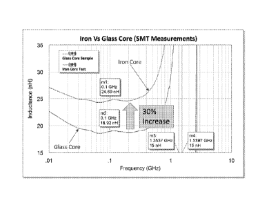
FIG. 2 is a graph that shows the results from using an RF circulator/isolator
device of the present
invention. Briefly, the inductor is a critical element in an RF circulator.
The inductance
determines the efficiency and size of the RF circulator. The iron core
inductor has enhanced
performance relative a glass or hollow core inductor reducing the size and
losses of an RF
Circulator or other RF devices including filters and isolators.
It is contemplated that any embodiment discussed in this specification can be
implemented with
respect to any method, kit, reagent, or composition of the invention, and vice
versa. Furthermore,
compositions of the invention can be used to achieve methods of the invention.
It will be understood that particular embodiments described herein are shown
by way of illustration
and not as limitations of the invention. The principal features of this
invention can be employed in
17
Date Recue/Date Received 2021-03-12
various embodiments without departing from the scope of the invention. Those
skilled in the art
will recognize, or be able to ascertain using no more than routine
experimentation, numerous
equivalents to the specific procedures described herein. Such equivalents are
considered to be
within the scope of this invention and are covered by the claims.
All publications and patent applications mentioned in the specification are
indicative of the level of
skill of those skilled in the art to which this invention pertains.
The use of the word -a" or -an" when used in conjunction with the term -
comprising" in the claims
and/or the specification may mean -one," but it is also consistent with the
meaning of -one or
more," -at least one," and -one or more than one." The use of the term -or" in
the claims is used to
mean -and/or" unless explicitly indicated to refer to alternatives only or the
alternatives are
mutually exclusive, although the disclosure supports a definition that refers
to only alternatives and
-and/or." Throughout this application, the term -about" is used to indicate
that a value includes the
inherent variation of error for the device, the method being employed to
determine the value, or the
variation that exists among the study subjects.
As used in this specification and claim(s), the words -comprising" (and any
form of comprising,
such as -comprise" and -comprises"), -having" (and any form of having, such as
-have" and
-has"), -including" (and any form of including, such as -includes" and -
include") or -containing"
(and any form of containing, such as -contains" and -contain") are inclusive
or open-ended and do
not exclude additional, unrecited elements or method steps. In embodiments of
any of the
compositions and methods provided herein, -comprising" may be replaced with -
consisting
essentially of' or -consisting of'. As used herein, the phrase -consisting
essentially of' requires
the specified integer(s) or steps as well as those that do not materially
affect the character or
function of the claimed invention. As used herein, the term -consisting" is
used to indicate the
presence of the recited integer (e.g., a feature, an element, a
characteristic, a property, a
method/process step or a limitation) or group of integers (e.g., feature(s),
element(s),
characteristic(s), property(ies), method/process steps or limitation(s)) only.
The term -or combinations thereof' as used herein refers to all permutations
and combinations of
the listed items preceding the term. For example, -A, B, C, or combinations
thereof' is intended to
include at least one of: A, B, C, AB, AC, BC, or ABC, and if order is
important in a particular
context, also BA, CA, CB, CBA, BCA, ACB, BAC, or CAB. Continuing with this
example,
expressly included are combinations that contain repeats of one or more item
or term, such as BB,
AAA, AB, BBC, AAABCCCC, CBBAAA, CABABB, and so forth. The skilled artisan will
understand that typically there is no limit on the number of items or terms in
any combination,
unless otherwise apparent from the context.
18
Date Recue/Date Received 2021-03-12
As used herein, words of approximation such as, without limitation, -about",
"substantial" or
"substantially" refers to a condition that when so modified is understood to
not necessarily be
absolute or perfect but would be considered close enough to those of ordinary
skill in the art to
warrant designating the condition as being present. The extent to which the
description may vary
.. will depend on how great a change can be instituted and still have one of
ordinary skilled in the art
recognize the modified feature as still having the required characteristics
and capabilities of the
unmodified feature. In general, but subject to the preceding discussion, a
numerical value herein
that is modified by a word of approximation such as -about" may vary from the
stated value by at
least 1, 2, 3, 4, 5, 6, 7, 10, 12 or 15%.
.. All of the compositions and/or methods disclosed and claimed herein can be
made and executed
without undue experimentation in light of the present disclosure. While the
compositions and
methods of this invention have been described in terms of preferred
embodiments, it will be
apparent to those of skill in the art that variations may be applied to the
compositions and/or
methods and in the steps or in the sequence of steps of the method described
herein without
departing from the scope of the invention. All such similar substitutes and
modifications apparent
to those skilled in the art are deemed to be within the scope of the invention
as defined by the
appended claims.
For each of the claims, each dependent claim can depend both from the
independent claim and
from each of the prior dependent claims for each and every claim so long as
the prior claim
provides a proper antecedent basis for a claim term or element.
19
Date Recue/Date Received 2021-03-12