Note: Descriptions are shown in the official language in which they were submitted.
CA 03059415 2019-10-08
WO 2018/191104 PCT/US2018/026337
METHOD OF WAFER BONDING OF DISSIMILAR THICKNESS DIE
BACKGROUND
1. Technical Field
[001] The present disclosure relates generally to fabrication of integrated
circuits (ICs),
semiconductor devices and other miniaturized devices, and more particularly,
to optimizing the
yield of die-to-wafer bonding processes involving dies with dissimilar
heights.
2. Discussion of Related Art
[002] A trend in IC fabrication has been the interconnection of ICs different
sizes, fabricated on
different size wafers, and offering different functions (i.e., analog,
digital, optical) and materials.
The ICs can be tested before stacking to allow Known Good Die (KGD) to be
combined to
improve yield. The economic success of this vertical stacking and vertical
interconnect approach
depends on the yield and cost of the stacking and interconnection being
favorable compared to
the yield and cost associated with the increased IC or system on a chip area.
A manufacturing
method for realizing this approach is to vertically stack ICs using direct
bond hybridization
(DBH), to form a covalent bond between wafers.
[003] One version of vertical stacking and vertical interconnection is where
ICs (on a substrate)
are bonded in a die-to-wafer (D2W) format where die are bonded IC-side down,
to a common
wafer IC-side up to allow the stacking of Known Good Die to improve yield. In
order to make
the cost of manufacturing an IC as small as possible, many instances of a
compound
semiconductor device (GaAs, InP, GaN, etc.) may be fabricated at one time on a
small
semiconductor wafer, typically 100mm in diameter. Typical foundry ICs are
fabricated on
200mm diameter silicon wafers. To utilize DBH wafer bonding with devices from
small wafers,
the devices need to be singulated into die, and then bonded to a 200mm wafer.
Chip dicing is the
process of dividing a wafer into multiple individual die, and typically
involves the use of a saw
blade, chemicals, a laser, or their combination to cut through and along kerf
regions that run
between multiple devices arranged on the wafer. Chip dicing can leave
aberrations that may
translate into yield lowering voids in following bonding processes. D2W
bonding is typically
very low yield, due to such particles generated during singulation and an
inability to re-polish
(e.g., CMP) the bond surface of the die due to handling limitations (i.e., in
order to handle a
wafer without breaking it, the wafer should have a thickness of at least 700
um). In addition,
1
CA 03059415 2019-10-08
WO 2018/191104 PCT/US2018/026337
manufacturers of multi-chip modules containing more than one die are becoming
very popular
because of their compactness and processing power. Manufacturers of such
packages are always
looking for ways to reduce the size or thickness of such packages. One way of
reducing the
thickness of such packages is to use die that are as thin as possible.
[004] While many methods exist for thinning an entire wafer, which is then
used in its entirety,
few methods exist for thinning individual die. Thus, what is needed is a D2W
manufacturing
process that accommodates use of dissimilarly sized, singulated die that
overcomes current
limitations.
SUMMARY
[005] In accordance with certain embodiments, a technique is provided for
bonding a plurality
of die that may have dissimilar thicknesses to a common wafer (e.g., having a
diameter of about
200 mm). The die may comprise direct bond hybridization (DBH) device
structures fabricated
and singulated from distinct device wafers (e.g., having diameters of about
100 mm) and a
planarized oxide layer. Each singulated die has a face side, a substrate
material back side, and a
thickness. Each die face side includes the planarized oxide layer, which
protects one or more
metallized post structures connecting to a device structure formed in the die.
[006] Each of a plurality of die may be bonded face side (circuit side) down
to a front side of a
first handle wafer, such that the metallized post structures associated with
each of the die lie in a
common plane. The plurality of die may be precisely aligned in the x-y
directions with a pick
and place instrument. The material substrate back sides of the bonded
plurality of die may be
thinned to a uniform thickness (e.g., through backgrinding and/or CMP, etc.),
and a silicon
dioxide layer may be deposit bonded on the thinned die back sides and on
exposed surfaces of
the first handle wafer. The back sides of the uniformly thinned plurality of
die may then be
bonded to a front side of a second handle wafer. The first handle may then be
removed, and the
planarized oxide layers may be removed from each face side of the plurality of
uniformly
thinned die to reveal the one or more metallized post structures.
[007] In certain embodiments, one or more of the die may exhibit a region of
potential
aberrations that could lead to yield-lowering voids in bonding steps, where
the regions result
from the dicing of the die from their respective device wafer(s). The regions
are generally
disposed in a plane adjacent the one or more metallized post structures in
each die (and between
the post structures and the die-bonded first handle front face in the interim
wafer assembly
2
CA 03059415 2019-10-08
WO 2018/191104
PCT/US2018/026337
structure.) The regions do not negatively impact the bonding of the face sides
of the die to the
first handle and, advantageously, the regions will be removed with the
protective planarized
oxide layer associated with each die. This significantly increases yield of
the process, wherein
Known Good Die may be bonded in the final composite wafer structure.
[008] In one embodiment, the process further includes fabrication of the die
device structures
on distinct device wafers, protecting each of the die device structures with
associated oxide
layers, and singulating the die. At least one of the device die may be a
compound semiconductor
device (e.g., GaAs, InP, GaN, etc.). The first and/or second handles may be
bonded to the die by
application of a low temperature oxide bonding process (such as the bonding
described in U.S.
Patent 8,053,329, the contents of which are incorporated by reference), by DBH
bonding, or by
application of an adhesive between the uniformly thinned die back sides and
first and second
handle front sides. The first and/or second handles may be remove by thinning,
resulting for the
second handle in exposure of the device die.
[009] In another embodiment, uniform thinning of the back sides of the die may
optionally be
preceded by filling in gaps between each of the die bonded to the first handle
with a strength
enhancing polymeric material prior to thinning to help maintain the relative
positioning of the die
during, for example, CMP processing. Then, the polymeric fill material may be
removed after
thinning, either prior to deposit bonding the SiO2 layer or after removing the
first handle wafer.
BRIEF DESCRIPTION OF THE FIGURES
[0010]
Various aspects of at least one embodiment of the present disclosure are
discussed
below with reference to the accompanying figures. It will be appreciated that
for simplicity and
clarity of illustration, elements shown in the drawings have not necessarily
been drawn
accurately or to scale. For example, the dimensions of some of the elements
may be exaggerated
relative to other elements for clarity or several physical components may be
included in one
illustrated element. Further, where considered appropriate, reference numerals
may be repeated
among the drawings to indicate corresponding or analogous steps or components.
For purposes
of clarity, not every component may be labeled in every drawing. The figures
are provided for
the purposes of illustration and explanation and are not intended as a
definition of the limits of
the invention. In the figures:
3
CA 03059415 2019-10-08
WO 2018/191104 PCT/US2018/026337
[0011] FIG. 1 is a flowchart of a method for die to wafer bonding of
dissimilar thickness die,
according to illustrative embodiments.
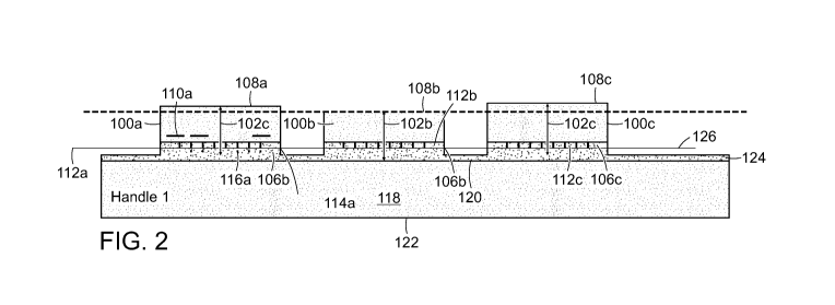
[0012] FIG. 2 schematically illustrates a step of bonding (or tacking) die
of dissimilar heights
to a first handle wafer;
[0013] FIG. 3 schematically illustrates a step of filling gaps between die
with a polymeric
material;
[0014] FIG. 4 schematically illustrates a step of backgrinding and/or CMP
to set all die
thicknesses to a uniform level;
[0015] FIG. 5 schematically illustrates a step of bonding (or tacking) a
second handle wafer to
the back sides of the die;
[0016] FIG. 6 schematically illustrates a step of flipping the wafer
structure to a preferred
orientation and removal of the first handle wafer; and
[0017] FIG. 7 schematically illustrates a step of removing a protective
planarized oxide layer
and potential debris regions form the die, and revealing the device die post
structures.
DETAILED DESCRIPTION
[0018] In the following detailed description, numerous specific details are
set forth in order
to provide a thorough understanding of the aspects of the present disclosure.
It will be
understood by those of ordinary skill in the art that these may be practiced
without independently
some of these specific details. In other instances, well-known methods,
procedures, components
and structures may not have been described in detail so as not to obscure the
embodiments. The
following descriptions of preferred embodiments are merely exemplary in nature
and is in no
way intended to limit the disclosure, its application, or uses. Also, it is to
be understood that the
phraseology and terminology employed herein are for the purpose of description
only and should
not be regarded as limiting. It is appreciated that certain features, are, for
clarity, described in
the context of separate embodiments but may also be provided in combination in
a single
embodiment. Conversely, various features are, for brevity, described in the
context of a single
embodiment but may also be provided separately or in any suitable sub-
combination.
[0019] No element, act, or instruction used herein should be construed as
critical or essential
unless explicitly described as such. Also, as used herein, the articles "a"
and "an" are intended to
include one or more items, and may be used interchangeably with "one or more."
Further, the
4
CA 03059415 2019-10-08
WO 2018/191104 PCT/US2018/026337
phrase "based on" is intended to mean "based, at least in part, on" unless
explicitly stated
otherwise. It will be further understood that the terms "comprise" (and any
form of comprise,
such as "comprises" and "comprising"), "have" (and any form of have, such as
"has", and
"having"), "include" (and any form of include, such as "includes" and
"including"), and
"contain" (and any form of contain, such as "contains" and "containing") are
open-ended linking
verbs. As a result, a method, structure or device that "comprises," "has,"
"includes," or
"contains" one or more steps or elements possesses those one or more steps or
elements, but is
not limited to possessing only those one or more steps or elements.
Furthermore, a device or
structure that is configured in a certain way is configured in at least that
way, but may also be
configured in ways that are not listed.
[0020] For purposes of the description hereinafter, the terms "upper",
"lower", "vertical",
"horizontal", "front side", "back side" and derivatives thereof shall relate
to the disclosed
structures and methods, as oriented in the drawing figures. The terms "on
top", "adjacent",
"positioned on" or "positioned atop" mean that a first element, such as a
first structure, is present
on or in proximity to a second element, such as a second structure, wherein
intervening elements,
such as an interface structure may be present between the first element and
the second element.
The term "direct contact" means that a first element, such as a first
structure, and a second
element, such as a second structure, are connected without any intermediary
conducting,
insulating or semiconductor layers at the interface of the two elements.
[0021] Referring to FIG. 1, there is illustrated an exemplary bonding
process 10 for
mounting a plurality of known good die with dissimilar thicknesses to a handle
wafer into a 3D
stack and then correcting wafer thickness variations by thinning back sides of
the die in a single
wafer level uniform thickness thinning process. As used herein, the term "die"
is used to refer to
a small piece of semiconducting material which has been fabricated (e.g., DBH
bond processing,
etc.) with a circuit. The term "base technology wafer" is used to refer to
integrated circuits,
semiconductor devices, and other miniaturized devices, including but not
limited to CMOS,
optoelectronics, infrared detectors, MEMS, and the like, which typically have
diameters of
approximately of 200 mm. The term "device wafer" is used to refer to a thin
slice of
semiconductor material used in the fabrication of integrated circuits,
semiconductor devices, and
other miniaturized devices, which have diameters smaller than the diameter of
base technology
wafers, typically on the order of 100mm. The term "handle wafer" is used to
refer to a wafer
CA 03059415 2019-10-08
WO 2018/191104 PCT/US2018/026337
that provides mechanical support to other components (e.g., singulated die)
while they are
processed and thinned. In most die-to-wafer (D2W) applications, electronic
components are
built in stages on one or more device wafers and on a base technology wafer.
For dissimilar size
device wafers and/or different materials, device wafers are diced, and the
singulated die are
aligned and bonded onto die sites of a receiving base technology wafer.
Conventional
techniques are very low yielding, due to the fact that singulated die pick up
debris from dicing
and handling and cannot be cleaned or prepped for bonding, since the die
cannot be loaded onto
a CMP tool for final polish. The disclosed techniques overcome such obstacles,
by thinning the
die after bonding to a silicon handle wafer that can be cleaned and polished,
and removing wafer
regions where such debris may be contained.
[0022] A composite structure comprising a (e.g., silicon) handle wafer
populated with
uniformly thinned KGD may be fabricated by bonding method 10 that may begin
with optional
steps 20 of fabricating a device wafer and a first and a second silicon handle
wafer and step 25 of
singulating the die. Then, method 10 continues with step 30 of temporarily
bonding the die to a
front side the first silicon handle wafer such that device post structures of
the die are aligned in a
common plane, step 35 of uniformly thinning the back sides of the bonded die,
which may
include an optional step 40 of filling gaps between the bonded die with a
mechanical stability
reinforcing polymeric material (e.g., BCB, polyimide, PR, etc.), step 45 of
deposit bonding a
silicon dioxide layer to the backside (back sides of thinned dies and exposed
surface areas of the
front side of first handle wafer, step 50 of bonding the back sides of the
thinned dies to a front
side of the second handle wafer, step 55 of removing the first handle wafer,
and step 60 of
revealing the device post structures of the die, where the process for
revealing the device post
structures includes removal of regions of potential singulation aberrations
that may contain
singulation and handling debris. These individual steps are described in
greater detail with
reference to FIGS. 2-7 hereinafter. In addition, optional further wafer
bonding per standard
processing may be performed after the final composite structure fabrication
step 65, for example,
to a base technology wafer.
[0023] FIGS. 2-7 schematically show a method or process for producing a
composite
structure comprising a (e.g., silicon) handle wafer populated with uniformly
thinned known good
die in accordance with method 10. FIGS. 2-7 may be considered successive
individual process
6
CA 03059415 2019-10-08
WO 2018/191104 PCT/US2018/026337
steps generally corresponding to the steps set forth in method 10 of FIG. 1,
for ease of
discussion.
[0024] As shown in in FIG. 2, one or more die 100a-100c having variable
(e.g., greater than 5
p.m) thicknesses 102a-102c may have been previously fabricated in a manner
known in the art on
one or more device wafers and singulated. Representative die 100a includes a
face (circuit) side
106a, a substrate material back side 108a, an integrated device structure 110a
(e.g., a DBH
structure), one or more metallized post structures 112a providing
interconnection to the
integrated device structure, and a protective planarized oxide layer 114a
covering the post
structures 112a. Within the planarized oxide layer 114a may be a region 116a
of potential
singulation and/or handling debris that, but for its subsequent removal by the
presently disclose
method 10, would otherwise lead to bonding voids and die to die variability in
bonding strength
due to an inability to properly CM' the composite die structure. A first
silicon handle 118
including a front side 120, a back side 122, and an oxide layer 124 at the
front side 120 may have
also been previously fabricated. The face sides 106a-106c of the die 100a-100c
and the front
side 120 of the first handle wafer 118 may be prepared and temporarily bonded,
such that the
respective post structures 112a-112c are aligned in a common plane 126. The
die 100a-110c
may be precisely aligned in the X-Y plane 126 using a pick and place
instrument, and may have
been previously tested to be known good die. Final Z-axis alignment of the die
back sides 108a-
108c will be achieved by grinding and CM'. The die 100a-100c may be bonded to
the front side
120 of first handle wafer 118 may be achieved through a low temperature oxide
bonding process
(e.g., ZiBond bonding offered by Tessera Technologies of San Jose,
California), by application
of a temporary adhesive (and appropriate heat and force) between the face
sides 106a-106c and
first wafer front side 120, allowing tacking thereto, or by similar
techniques. The temporary
adhesive may comprise sacrificial adhesives, thermoplastic, thermal cure, and
UV cure
adhesives, and may be applied by spin coating, or other known techniques.
[0025] Temporarily bonding the die 100a-100c to the first handle wafer 118
provides
necessary support in order to allow for thinning and processing of the die
back sides 108a-108c
without breaking, warping or folding of the die. With reference to FIG. 3,
optionally a polymeric
material 130 may be used to temporarily fill gaps 132 between the die 100a-
100c to a level 134
approximately equal to a final desired height of the die 100a-100c, if
additional mechanical
reinforcement is needed. This step may require annealing (e.g., 150 C) to
hold the location of
7
CA 03059415 2019-10-08
WO 2018/191104 PCT/US2018/026337
the material 130. As can be seen in FIG. 4, backgrinding and CMP may be
applied to the back
sides 108a-108c to thin the die 100a-100c to the final desired height 136. The
grinding and
thinning removes the substrate material from the back sides 108a-108c of the
die 100a-100c until
a desired thickness (e.g., 40 p.m) is achieved. The die thicknesses are
preferably controlled to
within 1 p.m to enable high yield bonding. If a polymeric fill material 130
has been employed, it
may be removed from the wafer assembly (e.g., through heat activation).
[0026] With reference to FIG. 5, the thinned back sides 108-108c of die
100a-100c and
exposed surfaces 136 of the front side 120 of the first handle wafer 118 may
be prepared with a
protective conformal coating 140, such as a silicon dioxide coating layer for
a silicon wafer. A
second handle wafer 142 may then be temporarily bonded to the prepared,
planarized back sides
108a-108c of die 100a-100c. Similar bonding processes as used to bond the
first wafer handle
118 to the die 100a-100c may be employed.
[0027] As shown in FIG. 6, an intermediate wafer assembly 144 may be
flipped to a preferred
orientation to allow processing on the first wafer handle 118. Backgrinding
and CMP may then
be applied to remove the first handle wafer 118 from the assembly, resulting
in exposure of the
protective planarized oxide layers 114a-114c covering the post structures 112a-
112c. As noted,
within the planarized oxide layers 114a-114c may be regions 116a-116c of
potential singulation
and/or handling debris. With reference to FIG. 7, if necessary another
polymeric fill 150 may be
applied to the gaps 132 prior to backgrinding and CMP of the protective
planarized oxide layers
114a-114c on face sides 106a-106c of the die in order to remove the planarized
oxide layers
114a-114c and the regions 116a-116c of potential debris, and to reveal the
metalized post
structures 112a-112c in common plane 126. If a polymer fill 150 was used, it
may be removed,
resulting in a final composite wafer structure that is ready for use in
subsequent standard wafer to
wafer bonding processes.
[0028] The method embodiments described above may employ existing tooling
and materials,
and provide advantages over currently used bonding methods including, but not
limited to, the
ability to integrate device dies of dissimilar thicknesses from different
technologies, e.g., CMOS,
optoelectronics, MEMS, and other microelectronic devices. In addition, the
yield of the resulting
devices may be increased by incorporating only known-good die into the devices
and the
elimination of potential die singulation and handling debris, thereby
significantly improving
yield. Furthermore, the ability to bond thin dies allows for the stacking of
multiple device layers,
8
CA 03059415 2019-10-08
WO 2018/191104
PCT/US2018/026337
including those from different technologies, connected vertically while
maintaining a low-profile
package.
[0029] It
will be understood that the architectural and operational embodiments
described
herein are exemplary of a plurality of possible arrangements to provide the
same general
features, characteristics, and general system operation. Modifications and
alterations will occur
to others upon a reading and understanding of the preceding detailed
description. It is intended
that the disclosure be construed as including all such modifications and
alterations. Thus, the
breadth and scope of the present disclosure should not be limited by any of
the above-described
exemplary embodiments, but should be defined only in accordance with the
following claims
appended hereto and their equivalents.
9