Note: Descriptions are shown in the official language in which they were submitted.
CA 03059508 2019-10-09
WO 2018/189205 PCT/EP2018/059205
Nanostructure
This invention concerns a process for growing semiconductor nanostructures
epitaxially on 13-Ga203 substrates, e.g. using molecular beam epitaxy or metal
organic vapour phase epitaxy (MOVPE) techniques to grow nanostructures
epitaxially on 0 -Ga203 substrates. The resulting nanostructures form a
further
aspect of the invention. The nanostructures are preferably semiconductor
materials
and have wide ranging applications in, for example, the electronics industry
or in
solar cell applications. The use of the composition in light-emitting diodes
(LEDs)
and photodetectors are especially preferred.
Background
Wide band-gap GaN and related ternary and quarternary 111-N
semiconductor compounds have been recognized to be among the most important
semiconductors for electronics and optoelectronic devices due to their
remarkable
optical, electrical and physical properties. Nevertheless, the
commercialization of
GaN-based devices is hampered by limited substrate availability. Si and
sapphire
(A1203) have been traditionally employed for their low-cost and good thermal
conductivity but these materials have a relatively large lattice- and thermal
expansion-mismatch with GaN.
13-Ga203 substrates have recently emerged as a substrate for III-nitride LED
and power devices due to their high transparency to light into the deep UV
(band
gap ¨4.8 eV (260 nm)) as well as being highly n-type conductive. 13-Ga203 may
therefore represent an alternative to sapphire (A1203) substrates that are
used for
most of today's III-nitride LEDs and power devices. Recently, E. G. Villora et
al,
proposes 13-Ga203 as a substrate for heteroepitaxial deposition of GaN and the
application of these materials in LEDs and power devices (Proc. SPIE 8987
89871U
(2014)). The GaN is here deposited as a thin-film.
However the lattice mismatch of 13-Ga203 on the (001) and (-201)-planes of
13-Ga203 with GaN is 2.6 % and 4.7%, respectively. Such lattice mismatch is a
major problem for III-nitride thin film growth. To solve this problem,
advanced
CA 03059508 2019-10-09
WO 2018/189205 PCT/EP2018/059205
- 2 -
buffer layers have to be used. Even then, the dislocation density can still be
as high
as 5 x 107 cm-2 for an InGaN epilayer grown on the (-201) plane of13-Ga203 (M.
M.
Muhammed, et al, High-quality III-nitride films on conductive, transparent (-
201)-
oriented 13-Ga203 using a GaN buffer layer, Scientific Reports 6, 27947,
(2016).
There remains a need therefore to develop alternative compositions that
solve the problem of lattice mismatch without the use of complex buffer
layers. One
solution is to use a substrate which is formed from the same material as the
semi-
conductor, e.g. a GaN substrate for a GaN semiconductor. Such substrates are
however very expensive and would limit the transparency to the near UV (band
gap
3.4 eV (365 nm)).
In order to overcome these problems this invention concerns the epitaxial
growth of semiconductor nanostructures, especially III-nitride nanostructures,
on 13-
Ga203 substrates and electronic devices such as LEDs comprising the
composition.
Rather than epitaxial growth of a thin film of semi-conductor group III-V
material
therefore, we propose a nanostructure, e.g. a nanowire or nanopyramid.
The bottom-up growth of nanostructures offers new opportunities to obtain
high quality heteroepitaxial group III-nitride materials on 13-Ga203. Unlike
in the
thin film solutions above, the inventors have appreciated that the lattice
mismatch
can be accommodated via the small cross-sectional area which the nanostructure
has
on the substrate. This induces elastic rather than plastic strain relaxation
at the free
surface extending into the nanostructure volume. The generated strain and
possible
misfit dislocations are confined to the nanostructure/substrate interface and
do not
affect the nanostructure itself. Thus, the crystal quality of the epitaxial
material is
nearly independent of the crystalline characteristics of the underlying
substrate. As a
consequence of its large aspect ratio, possible dislocation lines for
nanostructure
whose diameter exceeds its critical diameter tend to find its minimum energy
by
shortening its length in such a way that it bends towards the nanostructure
sidewalls
instead of propagating vertically in the [111] (for zinc blende III-V
semiconductor
nanostructures) or [0001] (for wurtzite III-V semiconductor nanostructures)
direction. This allows the upper part of the nanostructure to be free from
structural
defects.
CA 03059508 2019-10-09
WO 2018/189205 PCT/EP2018/059205
- 3 -
Since the crystal structure of13-Ga203 is monoclinic, with space group C2/m,
the symmetry is very low and very different from other common semiconductor
substrates that usually have a cubic or hexagonal crystal structures, which is
one of
the reasons it has not been considered as useful substrate until very
recently.
However on the (100) and (-201) planes of13-Ga203, the atomic arrangement is
close
to hexagonal and an epitaxial relation with the hexagonal atomic arrangement
of the
[111]-oriented zinc blende and [00011-oriented wurtzite semiconductor crystals
is
possible. Whilst the lattice-mismatch is still too large for high quality thin
film
growth, the use of nanostructures offers a way of growing virtually
dislocation-free
semiconductor devices based on the 13-Ga203 substrate
Nanostructures can accommodate much more lattice mismatch than thin
films due to their small footprint. Therefore, the growth of high quality,
dislocation-
free semiconductors nanostructures on the (100) and (-201) planes of13-Ga203
is
proposed. This can be achieved without the need for any advanced buffer
layers.
This is particularly attractive for the growth of III-nitride nanostructures,
where the
13-Ga203 substrate can be used as a transparent and conductive electrode for
LEDs,
such as vertical flip-chip LEDs, in particular UV LEDs emitting as short as at
¨ 280
nm.
Summary of Invention
Thus, viewed from one aspect the invention provides a composition of matter
comprising at least one nanostructure grown epitaxially on an optionally doped
0-
Ga203 substrate,
wherein said nanostructure comprises at least one group III-V compound.
Viewed from another aspect the invention provides a composition of matter
comprising:
at least one core semiconductor nanostructure grown epitaxially on an
optionally doped 13-Ga203 substrate wherein said nanostructure comprises at
least
one group III-V compound;
a semiconductor shell surrounding said core nanostructure, said shell
comprising at least one group III-V compound;
CA 03059508 2019-10-09
WO 2018/189205 PCT/EP2018/059205
- 4 -
said core semiconductor nanostructure being doped to form a n-type or p-
type semiconductor; and
said shell being doped to form a p-type or an a n-type semiconductor
opposite to said core; and
an outer conducting coating surrounding at least part of said shell which
forms an electrode contact.
Viewed from another aspect the invention provides a composition of matter
comprising:
at least one semiconductor nanostructure grown epitaxially on an optionally
doped 13-Ga203 substrate wherein said nanostructure comprises at least one
group
III-V compound;
said semiconductor nanostructure being doped such that the nanostructure
contains axial n-type and p-type semiconductor regions.
Viewed from another aspect the invention provides a process for preparing at
least one nanostructure grown epitaxially on an optionally doped 13-Ga203
substrate
comprising the steps of:
(I) providing group III-V elements to the surface of an optionally doped
13-Ga203 substrate; and
(II) epitaxially growing at least one nanostructure from the surface of the
13-Ga203 substrate.
Viewed from another aspect the invention provides a device, such as an
electronic device, comprising a composition as hereinbefore defined, e.g. a
solar cell
or LED.
Viewed from another aspect the invention provides a LED device
comprising:
a plurality of nanostructures grown epitaxially on a doped 13-Ga203 substrate,
said nanostructures having a p-n or p-i-n junction,
a first electrode in electrical contact with said doped 13-Ga203 substrate;
a second electrode in contact with the top of at least a portion of said
nanostructures optionally in the form of a light reflective layer;
wherein said nanostructures comprise at least one group III-V compound
semiconductor. In use, light is preferably emitted through the doped 13-Ga203
CA 03059508 2019-10-09
WO 2018/189205 PCT/EP2018/059205
- 5 -
substrate in a direction substantially parallel to but opposite from the
growth
direction of the nanostructures.
Viewed from another aspect, the invention provides a light emitting diode
device comprising:
a plurality of nanostructures grown epitaxially on a doped 13-Ga203 substrate,
preferably through the holes of an optional hole-patterned mask on said doped
0-
Ga203 substrate, said nanostructures having a p-n or p-i-n junction,
a first electrode in electrical contact with said doped 13-Ga203 substrate;
a light reflective layer in contact with the top of at least a portion of said
nanostructures or in contact with a second electrode in electrical contact
with the top
of at least a portion of said nanostructures, said light reflective layer
optionally
acting as the second electrode;
a second electrode in electrical contact with the top of at least a portion of
said nanostructures, said second electrode being essential where said light
reflective
layer does not act as an electrode;
wherein said nanostructures comprise at least one group III-V compound
semiconductor; and wherein in use light is emitted from said device through
the
doped 13-Ga203 substrate in a direction substantially opposite to said light
reflective
layer.
Viewed from another aspect, the invention provides a light emitting diode
device comprising:
a plurality of nanostructures grown epitaxially on a doped 13-Ga203 substrate,
preferably through the holes of an optional hole-patterned mask on said
substrate,
said nanostructures having a p-n or p-i-n junction,
a first electrode in electrical contact with said substrate;
a light reflective layer in contact with the top of at least a portion of said
nanostructures, said light reflective layer optionally acting as the second
electrode;
a second electrode in electrical contact with the top of at least a portion of
said nanostructures, said second electrode being essential where said light
reflective
layer does not act as an electrode;
wherein said nanostructures comprise at least one group III-V compound
semiconductor; and wherein in use light is emitted through the doped 13-Ga203
CA 03059508 2019-10-09
WO 2018/189205 PCT/EP2018/059205
- 6 -
substrate from said device in a direction substantially opposite to said light
reflective
layer.
Viewed from another aspect, the invention provides a nanostructured LED
comprising a plurality of group III-V compound semiconductor nanostructures
grown epitaxially on a doped 13-Ga203 substrate; wherein
each of the nanostructures protrudes from the substrate and each
nanostructure comprises a p-n or p-i-n-junction;
the top part of at least a portion of said nanostructures is covered with a
light-reflecting or transparent contact layer to form at least one contact to
group of
nanostructures;
an electrode is in electrical contact with said doped 13-Ga203 substrate;
the light-reflecting or transparent contact layer is in electrical contact
with
the first electrode via said nanostructures.
Viewed from another aspect, the invention provides use of an LED device as
hereinbefore defined as a LED, in particular in the UV region of the spectrum.
In a further embodiment, the invention relates to a photodetector. Rather
than emitting light, the device of the invention can be adapted to absorb
light and
subsequently generate a photocurrent and hence detect light.
Thus, viewed from another aspect the invention provides a photodetector
device comprising:
a plurality of nanostructures grown epitaxially on a doped 13-Ga203 substrate,
said nanostructures having a p-n or p-i-n junction,
a first electrode in electrical contact with said doped 13-Ga203 substrate;
a second electrode in contact with the top of at least a portion of said
nanostructures optionally in the form of a light reflective layer;
wherein said nanostructures comprise at least one group III-V compound
semiconductor; and wherein in use light is absorbed in said device.
Viewed from another aspect the invention provides a photodetector device,
such as a UV photodetector device, comprising:
a plurality of nanostructures grown epitaxially on an n(p)-doped 13-Ga203
substrate, said nanostructures being p(n)-doped;
a first electrode in electrical contact with said doped 13-Ga203 substrate;
CA 03059508 2019-10-09
WO 2018/189205
PCT/EP2018/059205
- 7 -
a second electrode in contact with the top of at least a portion of said
nanostructures optionally in the form of a light reflective layer;
wherein said nanostructures comprise at least one group III-N compound
semiconductor; and wherein in use light is absorbed in said device.
Viewed from another aspect the invention provides a nanostructured
photodetector comprising a plurality of group III-V compound semiconductor
nanostructures grown epitaxially on a doped 13-Ga203 substrate; wherein
each of the plurality of nanostructures protrudes from the substrate and each
nanostructure comprises a p-n- or p-i-n-junction;
a top portion of each nanostructure or at least one group of nanostructures
from the plurality of nanostructures is covered with a transparent contact
layer to
form at least one contact to group of nanostructures;
an electrode is in electrical contact with said doped 13-Ga203 substrate;
the transparent contact layer is in electrical contact with the first
electrode
via the p-n or p-i-n-junction in said nanostructures.
Viewed from another aspect, the invention provides use of a photodetector
device as hereinbefore defined as a photodetector, in particular in the deep
UV
region of the spectrum (a so called solar blind photodetector).
Definitions
By a group III-V compound is meant one comprising at least one ion from
group III and at least one ion from group V. There may be more than one
element
present from each group, e.g. AlGaN (i.e. a ternary compound), AlInGaN (i.e. a
quaternary compound), and so on. The designation Al(In)GaN implies either
AlGaN or AlInGaN, i.e. that the presence of In is optional. Any element
indicated
in brackets may or may not be present.
The term nanostructure is used to apply to a nanowire or a nanopyramid.
The term nanowire is used herein to describe a solid, wire-like structure of
nanometer dimensions. Nanowires preferably have an even diameter throughout
the
majority of the nanowire, e.g. at least 75% of its length. The term nanowire
is
intended to cover the use of nanorods, nanopillars, nanocolumns or
nanowhiskers
CA 03059508 2019-10-09
WO 2018/189205 PCT/EP2018/059205
- 8 -
some of which may have tapered structures. The nanowires can be said to be in
essentially in one-dimensional form with nanometer dimensions in their width
or
diameter and their length typically in the range of a few 100 nm to a few pm.
Ideally the nanowire diameter is between 50 and 500 nm, however, the diameter
can
exceed few microns (called microwires).
Ideally, the diameter at the base of the nanowire and at the top of the
nanowire should remain about the same (e.g. within 20% of each other).
The term nanopyramid refers to a solid pyramidal type structure. The term
pyramidal is used herein to define a structure with a base whose sides taper
to a
single point generally above the centre of the base. It will be appreciated
that the
single vertex point may appear chamferred. The nanopyramids may have multiple
faces, such as 3 to 8 faces, or 4 to 7 faces. Thus, the base of the
nanopyramids
might be a square, pentagonal, hexagonal, heptagonal, octagonal and so on. The
pyramid is formed as the faces taper from the base to a central point (forming
therefore triangular faces). The triangular faces are normally terminated with
(1-
101) or (1-102) planes. The triangular side surfaces with (1-101) facets could
either
converge to a single point at the tip or could form a new facets ((1-102)
planes)
before converging at the tip. In some cases, the nanopyramids are truncated
with its
top terminated with {0001} planes. The base itself may comprise a portion of
even
cross-section before tapering to form a pyramidal structure begins. The
thickness of
the base may therefore be up to 200 nm, such as 50 nm.
The base of the nanopyramids can be 50 and 500 nm in diameter across its
widest point. The height of the nanopyramids may be 200 nm to a few microns,
such as 400 nm to 1 micron in length.
It will be appreciated that the substrate preferably comprises a plurality of
nanostructures. This may be called an array of nanostructures.
The term epitaxy comes from the Greek roots epi, meaning "above", and
taxis, meaning "in ordered manner". The atomic arrangement of the nanowire is
based on the crystallographic structure of the substrate. It is a term well
used in this
art. Epitaxially growth means herein the growth on the substrate of a nanowire
that
mimics the orientation of the substrate.
CA 03059508 2019-10-09
WO 2018/189205
PCT/EP2018/059205
- 9 -
Epitaxial growth will preferably occur when the growth occurs from the (-
201) or (100) plane of the 13-Ga203 substrate.
Nanostructures can be grown using a catalyst if desired, e.g. via a vapour-
metal catalyst assisted liquid-solid (VLS) method. It is preferred however if
no
catalyst is used. Selective area growth (SAG) is the most promising method for
growing positioned nanostructures. This method is different from the metal
catalyst
assisted vapour-liquid-solid (VLS) method, in which metal catalyst act as
nucleation
sites for the growth of nanowires or nanopyramids. Other catalyst-free methods
to
grow nanostructures are self-assembly growth, spontaneous growth, and so on,
where nanostructures are nucleated in random positions on the 13-Ga203
substrate.
These methods yield fluctuations in the length and diameter of the
nanostructures.
The SAG method typically requires a mask with nano-hole patterns on the
substrate. The nanostructures nucleate in the holes of the patterned mask on
the
substrate. This yields uniform size and pre-defined position of the
nanostructures.
The term mask refers to the mask material that is directly deposited on the
substrate. The mask material should ideally not absorb emitted light (which
could be
visible, UV-A, UV-B or UV-C) in the case of an LED or not absorb the entering
light of interest in the case of a photodetector. The mask should also be
electrically
non-conductive. The mask could contain one or more than one material, which
include A1203, 5i02, Si3N4, TiO2, W203, and so on. Subsequently, the hole
patterns
in the mask material can be prepared using electron beam lithography or
nanoimprint lithography and dry or wet etching.
MBE is a method of forming depositions on crystalline substrates. The MBE
process is performed by heating a crystalline substrate in a vacuum so as to
energize
the substrate's lattice structure. Then, an atomic or molecular mass beam(s)
is
directed onto the substrate's surface. The term element used above is intended
to
cover application of atoms, molecules or ions of that element. When the
directed
atoms or molecules arrive at the substrate's surface, the directed atoms or
molecules
encounter the substrate's energized lattice structure as described in detail
below.
Over time, the incoming atoms form a nanostructure.
MOVPE also called as metal organic chemical vapour deposition (MOCVD)
is an alternative method to MBE for forming depositions on crystalline
substrates.
CA 03059508 2019-10-09
WO 2018/189205
PCT/EP2018/059205
- 1 0 -
In case of MOVPE, the deposition material is supplied in the form of metal
organic
precursors, which on reaching the high temperature substrate decompose leaving
atoms on the substrate surface. In addition, this method requires a carrier
gas
(typically H2 and/or N2) to transport deposition materials (atoms/molecules)
across
the substrate surface. These atoms reacting with other atoms form an epitaxial
layer
on the substrate surface. Choosing the deposition parameters carefully results
in the
formation of a nanowire or nanopyramid.
The notation n(p)-type doping implies n type or in the alternative p type
doping. Where nanostructures comprise a p-n- or p-i-n-junction, the order of
the
junction is not specified. For example, a p-i-n junction can be present in a
nanowire
irrespective of whether the p or n doping region is nearest the substrate. In
other
words the terms p-n or p-i-n and n-p or n-i-p are the same.
Detailed Description of Invention
This invention concerns the epitaxial growth of nanostructures on a 13-Ga203
substrate, especially a doped 13-Ga203 substrate. The composition of the
invention
comprises both the substrate and the nanostructures grown epitaxially thereon.
Having a nanostructure grown epitaxially provides homogeneity to the
formed material which may enhance various end properties, e.g. mechanical,
optical
or electrical properties.
Epitaxial nanostructures may be grown from gaseous or liquid precursors.
Because the substrate acts as a seed crystal, the deposited nanowire can take
on a
lattice structure and orientation identical to those of the substrate. This is
different
from thin-film deposition methods which deposit polycrystalline or amorphous
films, even on single-crystal substrates.
Substrate
The substrate for nanostructure growth is 13-Ga203. The crystal structure is
depicted in figure 5. Figure 6 also provides details of this material. These
substrates
CA 03059508 2019-10-09
WO 2018/189205 PCT/EP2018/059205
- 11 -
can be purchased in wafer sizes of 2" from commercial suppliers. The wafers
are
sufficiently thick that they are self-supporting and no separate support is
required.
In order to prepare nanostructures of commercial importance, it is essential
that these grow epitaxially on the substrate and without the formation of
dislocations
due to lattice mismatch. It is also ideal if growth occurs perpendicular to
the
substrate and ideally therefore in the [111] direction for zinc blende III-V
semiconductor nanostructures or [0001] direction for wurtzite III-V
semiconductor
nanostructures. It is especially preferred if the nanostructures are grown
from the (-
201) plane of the 13-Ga203 substrate.
There is no guarantee that growth is possible with a particular substrate
where that substrate material is different from the nanostructure being grown.
The
present inventors have determined, however, that epitaxial growth is possible
by
determining a possible lattice match between the atoms in the semiconductor
nanostructure and the atoms in the substrate. In particular, for GaN and13-
Ga203
substrate with surface (100) or (-201) plane the lattice mismatch is 2.6 % and
4.7 %,
respectively. It is preferred therefore if the lattice mismatch is less than 5
%.
In order to initiate the III-nitride nanostructure growth, e.g. on the (100)-
plane of13-Ga203, a nitridation step may be employed. This will substitute the
oxygen atoms at the surface of the substrate with nitrogen so that the
hexagonal
arrangement of the underlying Ga atoms is exposed and a first nano-epitaxial
GaN
monolayer can be formed. Nitridation can be achieved using ammonia (NH3)
(using
MOVPE or MBE growth methods) or nitrogen plasma source (using MBE growth
methods). Temperatures above 800 C and pressures of 102 Pa or more can be
employed for the nitridation in ammonia (NH3)-based MBE.
In the case of III-nitride nanostructures grown on the (-201)-plane of 0-
Ga203, a nitridation step might not be needed since the surface oxygen atoms
already form the hexagonal arrangement needed to induce the first nano-
epitaxial
III-nitride monolayer.
When MBE is used, the III-nitride nanostructure can be grown after the
optional nitridation step, at a typical temperature of around 800 C using
nitrogen
plasma source under N-rich conditions (similar growth conditions to typical
III-
nitride nanostructure growth on sapphire or silicon substrates). When MOVPE is
CA 03059508 2019-10-09
WO 2018/189205 PCT/EP2018/059205
- 12 -
used, a few nm thin GaN buffer may first be grown at 450- 550 C in a nitrogen
ambient, to prevent a chemical reaction of the fl-Ga203 substrate with
hydrogen
above 600 C. Temperatures typically around 1000 C, and a flow rate of
ammonia
(NH3) of around 5-100 sccm, in a hydrogen and/or nitrogen ambient can be used
for
the subsequent III-nitride nanostructure growth (similar growth conditions to
typical
III-nitride nanostructure growth on sapphire or silicon substrates).
Viewed from one aspect therefore, the invention allows for the substrate to
be treated with a nitridation step before growth of the nanostructures. A
nitridation
step typically introduces a nitride layer a few nm thick, e.g. up to 5 nm
thick, onto
the substrate.
In an alternative to the nitridation process, a buffer/nucleation layer can be
transferred, or grown on the substrate, e.g. a GaN buffer layer can be grown
on top
of the Ga203 at temperature around 550 C to provide a surface on which
nanowire
growth is initiated. Buffer layers of interest are based on group III-V
compounds,
such as GaN. The thickness of the grown buffer layer can vary from one atomic
thickness to even millimetre scale, such as 10 nm to 500 nm. The buffer layer
can be
applied by direct epitaxial growth or the buffer layer can be transferred on
top of the
13-Ga203 substrate, e.g. via a transfer method to place a GaN buffer layer on
top of 0-
Ga203 substrate. The buffer layer is preferably a nitride. The buffer layer is
preferably a binary nitride.
In one embodiment, a hole patterned mask layer is used on top of the
substrate. Where such a mask layer is used, the buffer may be located on top
of the
substrate and within the holes of the hole patterned mask.
Viewed from one aspect therefore, the invention provides a composition of
matter comprising at least one nanostructure grown epitaxially on a substrate
comprising a group III-V compound buffer layer, such as a GaN buffer layer,
and an
optionally doped 13-Ga203 layer,
wherein said nanostructure comprises at least one group III-V compound.
Viewed from another aspect the invention provides a composition of matter
comprising at least one nanostructure grown epitaxially on a substrate
comprising an
optionally doped 13-Ga203 layer, said substrate carrying a hole patterned mask
layer
through which said nanostructures are grown,
CA 03059508 2019-10-09
WO 2018/189205 PCT/EP2018/059205
- 13 -
wherein said nanostructure comprises at least one group III-V compound and
wherein the bottom of the holes of the hole patterned mask layer adjacent the
substrate are coated in a group III-V compound buffer, such as a GaN buffer.
Viewed from another aspect, the invention provides a process for preparing
at least one nanostructure grown epitaxially on an optionally doped 13-Ga203
substrate comprising the steps of:
(I) providing group III-V elements to the surface of a 13-Ga203 substrate
having a group III-V compound buffer layer applied thereto; and
(II) epitaxially growing at least one nanostructure from the surface of the
substrate.
Alternatively, viewed, it could be considered that a buffer present within the
holes of the mask forms part of the nanostructure.
Any buffer layer that is used preferably grows epitaxially on the substrate.
It
is possible to dope the buffer layer using doping techniques as herein
described for
other layers of the composition of matter, e.g. n-type dope the buffer layer.
Doping
of the buffer layer and/or corresponding doping of the 13-Ga203 substrate can
allow
the formation of p-n or p-i-n junctions in the substrate/buffer layer
structure and the
nanostructures. It will be appreciated that the nanostructures are grown from
the
buffer layer surface of the substrate, i.e. the buffer layer provides a
surface from
which nanostructures can grow.
Before growing any buffer layer it is preferred if the substrate is thermally
cleaned.
It is especially preferred if an epitaxial (Al, In)GaN buffer layer is used,
especially an n-type epitaxial (Al, In)GaN buffer layer.
It will be appreciated that the 13-Ga203 substrate is preferably doped. For
most devices, the substrate will be doped, e.g. n-doped. This can be achieved
by
doping with Sn or Si by the substrate producer.
Growth of Nanostructures
In order to prepare nanostructures of commercial importance, it is preferred
that these grow epitaxially on the substrate. It is also ideal if growth
occurs
CA 03059508 2019-10-09
WO 2018/189205 PCT/EP2018/059205
- 1 4 -
epitaxially and perpendicular to the substrate and ideally therefore in the
[111]-
direction for zinc blende III-V semiconductors or [0001]-direction for
wurtzite III-V
semiconductor crystals.
The present inventors have determined that high-quality epitaxial III-V
semiconductor nanostructure growth on the 13-Ga203 substrate is possible due
to the
small lattice match between the atoms in the semiconductor and the atoms in
the
substrate and the small footprint of the nanostructure on the substrate.
In a growing nanopyramid, the triangular faces are normally terminated with
(1-101) or (1-102) planes. The triangular side surfaces with (1-101) facets
could
either converge to a single point at the tip or could form a new facets ((1-
102)
planes) before converging at the tip. In some cases, the nanopyramids are
truncated
with its top terminated with {0001} planes.
Whilst it is ideal that there is no lattice mismatch between a growing
nanostructure and the substrate, nanostructures can accommodate much more
lattice
mismatch than thin films. The nanowires or nanopyramids of the invention may
have a lattice mismatch of up to about 10 % with the substrate and epitaxial
growth
is still possible. Ideally, lattice mismatches should be 7.5% or less, e.g. 5%
or less.
For some semiconductors like GaN (a = 3.189 A) and AN (a = 3.111 A), the
lattice mismatch is so small (<5%) that excellent growth of these
semiconductor
nanowires or nanopyramids can be expected on the (100) and (-201) planes of f3-
Ga203.
Growth of nanostructures can be controlled through flux ratios. Group III-
nitride nanopyramids are encouraged, for example if high N flux is employed.
The nanowires grown in the present invention may be from 250 nm to
several microns in length, e.g. up to 5 gm, such as 2 gm. Preferably the
nanowires
are at least 1 gm in length. Where a plurality of nanowires are grown, it is
preferred
if they all meet these dimension requirements. Ideally, at least 90% of the
nanowires grown on a substrate will be at least 1 micron in length. Preferably
substantially all the nanowires will be at least 1 gm in length.
Nanopyramids may be 250 nm to 1 micron in height, such as 400 to 800 nm
in height, such as about 500 nm.
CA 03059508 2019-10-09
WO 2018/189205 PCT/EP2018/059205
- 15 -
Moreover, it will be preferred if the nanostructures grown have the same
dimensions, e.g. to within 10% of each other. Thus, at least 90% (preferably
substantially all) of the nanostructures on a substrate will preferably be of
the same
diameter and/or the same length (i.e. to within 10% of the diameter/length of
each
other). Essentially, therefore the skilled man is looking for homogeneity and
nanostructures that are substantially the same in terms of dimensions.
The length of the nanostructures is often controlled by the length of time for
which the growing process runs. A longer process typically leads to a (much)
longer
nanowire or nanopyramid.
The nanowires have typically a hexagonal cross sectional shape. The
nanowire may have a cross sectional diameter of 25 nm to several hundred nm
(i.e.
its thickness). Diameters typically will not exceed 400 nm, such as 200 nm. As
noted above, the diameter is ideally constant throughout the majority of the
nanowire. Nanowire diameter can be controlled by the manipulation of the ratio
of
the atoms used to make the nanowire as described further below.
Moreover, the length and diameter of the nanostructures can be affected by
the temperature at which they are formed. Higher temperatures encourage high
aspect ratios (i.e. longer and/or thinner nanowires or nanopyramids). The
diameter
can also be controlled by manipulating the nanohole opening size of the mask
layer.
The skilled man is able to manipulate the growing process to design
nanostructures
of desired dimensions.
The nanostructures of the invention are formed from at least one III-V
compound semiconductor. Preferably, the nanostructure consists of group III-V
compounds only optionally doped as discussed below. Note that there may be
more
than one different group III-V compound present but it is preferred if all
compounds
present are group III-V compounds.
Group III element options are B, Al, Ga, In, and Tl. Preferred options here
are Ga, Al and In.
Group V options are N, P, As, Sb. All are preferred, especially N.
It is of course possible to use more than one element from group III and/or
more than one element from group V. Preferred compounds for nanowire or
nanopyramid manufacture include AlAs, GaSb, GaP, BN, GaN, AN, AlGaN,
CA 03059508 2019-10-09
WO 2018/189205 PCT/EP2018/059205
- 1 6 -
AlGaInN, GaAs, InP, InN, InGaN, InGaAs, InSb, InAs, or AlGaAs. Compounds
based on Al, Ga and In in combination with N are most preferred. The use of
GaN,
AlGaN, InGaN, AlInGaN or AN is highly preferred.
It is most preferred if the nanostructures consist of Ga, Al, In and N (along
with any doping atoms as discussed below).
Whilst the use of binary materials is possible, the use of ternary nanowires
or
nanopyramids in which there are two group III cations with a group V anion are
preferred here, such as AlGaN. The ternary compounds may therefore be of
formula
XYZ wherein X is a group III element, Y is a group III different from X, and Z
is a
group V element. The X to Y molar ratio in XYZ is preferably 0.1 to 0.9, i.e.
the
formula is preferably XxYl_xZ where subscript x is 0 to 1.
Quaternary systems might also be used and may be represented by the
formula AxBi_x_yCyD where A, B and C are different group III elements and D is
a
group V element. Again subscripts x and y are typically 0 to 1. Other options
will
be clear to the skilled man.
The growth of GaN, AlGaN, InGaN and AlInGaN nanostructures is
especially preferred. The wavelength of light emitted by a device containing
these
nanostructures can be tailored by manipulating the content of Al, In and Ga.
Alternatively, the pitch and/or diameter of the nanowires or nanopyramids can
be
varied to change the nature of the light emitted.
It is further preferred if the nanowires or nanopyramids contain regions of
differing compounds. The nanowire or nanopyramid might therefore contain a
region of a first group III-V semiconductor such as GaN followed by a region
of a
different III-V semi-conductor such as AlGaN. Nanostructures can contain
multiple
regions such as two or more or three or more. These regions might be layers in
an
axially grown nanowire or shells in a radially grown nanowire or nanopyramid.
It is especially preferred if the group III-V semiconductor grows with a
[111]-oriented zinc blende or [00011-oriented wurtzite crystal structure.
Doping
CA 03059508 2019-10-09
WO 2018/189205 PCT/EP2018/059205
- 17 -
The nanostructures of the invention are preferably doped, e.g. p-type doped,
especially p-type and n-type doped, e.g. so as to contain a p-n or p-i-n
junction. It is
also possible to dope the substrate and dope the nanostructure to create a p-n
junction between the two. Devices of the invention, especially those based on
a p-i-
n junction are therefore optionally provided with an undoped intrinsic
semiconductor region between a p-type semiconductor and an n-type
semiconductor
region. The doped top part region is typically heavily doped because it is
used for an
ohmic contact. The doped 13-Ga203 substrate will normally form the other ohmic
contact in a device, which allows for a vertical device configuration.
It is therefore preferred that the nanowires or nanopyramids are doped.
Doping typically involves the introduction of impurity ions into the nanowire
or
nanopyramid, e.g. during MBE or MOVPE growth. The doping level can be
controlled from ¨ 1015/cm3to 1020/cm3. The nanowires or nanopyramids can be p-
doped or n-doped as desired. Doped semiconductors are extrinsic conductors.
The n(p)-type semiconductors have a larger electron (hole) concentration
than hole (electron) concentration by doping an intrinsic semiconductor with
donor
(acceptor) impurities. Suitable donor (acceptors) for III-V compounds,
especially
nitrides, can be Si (Mg, Be and Zn). Dopants can be introduced during the
growth
process or by ion implantation of the nanowires or nanopyramids after their
formation.
The nanostructures of the invention can be grown to have a heterostructured
form radially or axially. For example for an axial heterostructured nanowire
or
nanopyramid, p-n junction can be axially formed by growing a p-type doped core
first, and then continue with an n-doped core (or vice versa). The core of the
nanostructure should normally have the same doping type as the 13-Ga203
substrate
(that is n(p)-type core on n(p)-type substrate). An intrinsic region can be
positioned
between doped cores for a p-i-n nanowire or nanopyramid. For a radially
heterostructured nanostructure, p-n junction can be radially formed by growing
the
p-doped nanowire or nanopyramid core first, and then the n-doped
semiconducting
shell is grown (or vice versa). An intrinsic shell can be positioned between
doped
regions for a p-i-n nanowire or nanopyramid.
CA 03059508 2019-10-09
WO 2018/189205 PCT/EP2018/059205
- 18 -
It is preferred if the nanostructures are grown axially and are therefore
formed from a first section and a second section axially up the nanostructure.
The
two sections are doped differently to generate a p-n junction or p-i-n
junction. The
top or bottom section of the nanostructures is the p-doped or n-doped section.
In a p-i-n nanostructure, when charge carriers are injected into the
respective
p- and n-regions, they recombine in the i-region, and this recombination
generates
light. In a p-n junction case, recombination will occur in the space charge
region (as
there is no intrinsic region). The light is generated inside each nanowire or
nanopyramid randomly and emitted in all directions. One problem with such a
structure is that a substantial fraction of the generated light is wasted, as
only a
portion is directed in a desired direction.
The use therefore of a light reflective layer ensures that the emitted light
is
directed out from the device in a desired direction, in particular opposite to
the
reflective layer.
The nanostructures of the invention preferably grow epitaxially. They attach
to the underlying substrate through a complex mixture of quasi van der Waals,
ionic
and covalent binding with the 13-Ga203 substrate. Accordingly, at the junction
of the
substrate and the base of the nanowire or nanopyramid, crystal planes are
formed
epitaxially within the nanowire or nanopyramid. These build up, one upon
another,
in the same crystallographic direction thus allowing the epitaxial growth of
the
nanostructure. Preferably the nanowires grow vertically. The term vertically
here is
used to imply that the nanowires grow perpendicular to the substrate. It will
be
appreciated that in experimental science the growth angle may not be exactly
90
but the term vertically implies that the nanowires are within about 100 of
vertical/perpendicular, e.g. within 5 . Because of the epitaxial growth via
covalent
bonding, it is expected that there will be an intimate contact between the
nanostructures and the 13-Ga203 substrate.
It will be appreciated that the substrate comprises a plurality of
nanostructures. Preferably the nanostructures grow about parallel to each
other. It
is preferred therefore if at least 90%, e.g. at least 95%, preferably
substantially all
nanostructures grow in the same direction from the same plane of the
substrate.
CA 03059508 2019-10-09
WO 2018/189205
PCT/EP2018/059205
- 19 -
It will be appreciated that there are mainly two planes within the 13-Ga203
substrate from which epitaxial growth could occur ((100) and (-201)). It is
preferred
if substantially all nanostructures grow from the same plane. It is preferred
if that
plane is parallel to the substrate surface. Ideally the grown nanostructures
are
substantially parallel. Preferably, the nanostructures grow substantially
perpendicular to the 13-Ga203 substrate.
The nanostructures of the invention should preferably grow in the [111]-
direction for zinc blende III-V semiconductors or [0001]-direction for
wurtzite III-V
semiconductor crystals.
The nanostructures are preferably grown by MBE or MOVPE. In the MBE
method, the substrate is provided with a molecular beam of each reactant, e.g.
a
group III element and a group V element preferably supplied simultaneously. A
higher degree of control of the nucleation and growth of the nanostructures on
the
substrate might be achieved with the MBE technique by using migration-enhanced
epitaxy (MEE) or atomic-layer MBE (ALMBE) where e.g. the group III and V
elements can be supplied alternatively.
A preferred technique in case of nitrides is plasma assisted solid-source
MBE, in which very pure elements such as gallium, aluminium, and indium are
heated in separate effusion cells, until they begin to slowly evaporate. The
rf-
plasma nitrogen source is typically used to produce low energy beams of
nitrogen
atoms. The gaseous elements then condense on the substrate, where they may
react
with each other. In the example of gallium and nitrogen, single-crystal GaN is
formed. The use of the term "beam" implies that evaporated atoms (e.g.
gallium)
and nitrogen atoms from the plasma source do not interact with each other or
vacuum chamber gases until they reach the substrate. Ammonia (NH3) might be
needed for an initial nitridation step if the III-nitride nanostructures
growth is done
by MBE on the (100) plane of the 13-Ga203 substrate.
MBE takes place in ultra high vacuum, with a background pressure of
typically around 10-10 to 10-9 Torr. Nanostructures are typically grown
slowly, such
as at a speed of up to a few pm per hour. This allows nanostructures to grow
epitaxially and maximises structural performance.
CA 03059508 2019-10-09
WO 2018/189205
PCT/EP2018/059205
- 20 -
The nature of the light emitted is a function of the diameter and composition
of the nanostructures. In order to tune the band gap of the nanostructure,
temperature and fluxes can be used.
In the MOVPE method, the substrate is kept in a reactor in which the
substrate is provided with a carrier gas and a metal organic gas of each
reactant, e.g.
a metal organic precursor containing a group III element and a metal organic
precursor containing a group V element. The typical carrier gases are
hydrogen,
nitrogen, or a mixture of the two. A higher degree of control of the
nucleation and
growth of the nanostructures on the substrate might be achieved with the MOVPE
technique by using pulsed layer growth technique, where e.g. the group III and
V
elements can be supplied alternatively.
Selective area growth of nanowires or nanopyramids
The nanostructures of the invention are preferably grown by selective area
growth (SAG) method. This method may require a mask with nano-hole patterns
deposited on the fl-Ga203 substrate.
In order to prepare a more regular array of nanostructures with better
homogeneity in height and diameter of grown nanostructures, the inventors
envisage
the use of a mask on the fl-Ga203 substrate. This mask can be provided with
regular
holes, where nanostructures can grow homogeneously in size in a regular array
across the substrate. The hole patterns in the mask can be easily fabricated
using
conventional photo/e-beam lithography or nanoimprinting. Thus a mask can be
applied to the substrate and etched with holes exposing the substrate surface,
optionally in a regular pattern. Moreover, the size and the pitch of the holes
can be
carefully controlled. By arranging the holes regularly, a regular pattern of
nanostructures can be grown.
Moreover, the size of the holes can be controlled to ensure that only one
nanostructure can grow in each hole. Finally, the holes can be made of a size
where
the hole is sufficiently large to allow nanostructure growth. In this way, a
regular
array of nanostructures can be grown.
CA 03059508 2019-10-09
WO 2018/189205 PCT/EP2018/059205
-21 -
By varying the size of the holes, one could control the size of the
nanostructure. By varying the pitch of the holes, one could optimize the light
extraction of light from the nanostructures.
The mask material can be any material which does not damage the
underlying substrate when deposited. The mask should also be transparent to
the
emitted light (LED) and entering light (photodetector). The minimum hole size
might be 50 nm, preferably at least 100-200 nm. The thickness of the mask can
be
to 100 nm, such as 10 to 40 nm.
The mask itself can be made of an inert compound, such as silicon dioxide or
10 silicon nitride. In particular, the hole-patterned mask comprises at
least one
insulating material such as SiO2, Si3N4, Hf02, TiO2 or A1203 e.g. deposited by
e-
beam evaporation, CVD, PE-CVD, sputtering, or ALD. The mask can therefore be
provided on the substrate surface by any convenient technique such as by
electron
beam deposition, CVD, plasma enhanced-CVD, sputtering, and atomic layer
deposition (ALD).
The use of a Ti mask that is either nitridated/oxidized before the nanowire
growth, is particularly preferred as such a mask has been found to allow
growth of
uniform nanostructures.
In a further embodiment, the invention may involve the transfer of a hole-
patterned mask of graphene/SiO2 or graphene/Si3N4 where graphene is closest to
the
Ga203 substrate. That is a mask with holes through both the graphene and the
second layer (e.g. SiO2 or Si3N4). Growth would happen through the holes from
Ga203 and the mask would protect the rest of the Ga203 during growth.
The selective area growth method yields nanostructures of uniform length,
and diameter at predefined positions. The nanostructures can also be grown
without
mask with nano-hole patterns. In such case, the nanostructures will have non-
uniform sizes (length and diameter), and located at random positions.
For the nanostructure growth, the substrate temperature can then be set to a
temperature suitable for the growth of the nanostructure in question. The
growth
temperature may be in the range 300 to 1000 C. The temperature employed is,
however, specific to the nature of the material in the nanowire or nanopyramid
and
the used method (MBE vs. MOVPE). For example in MBE, a preferred temperature
CA 03059508 2019-10-09
WO 2018/189205 PCT/EP2018/059205
- 22 -
for GaN nanostructure growth is 700 to 950 C, e.g. 700 to 850 C, such as 765
C.
For AlGaN the range is slightly higher, for example 800 to 980 C, such as 830
to
950 C, e.g. 850 C.
It will be appreciated therefore that the nanostructures can comprise
different
group III-V semiconductors within the nanostructure, e.g. starting with a GaN
stem
followed by an AlGaN component or AlGaInN component and so on.
For III-nitride nanostructure growth by MBE, it can be initiated by opening
the shutter of the Ga effusion cell, the nitrogen plasma cell, and the dopant
cell
simultaneously initiating the growth of doped GaN nanowires or nanopyramids,
hereby called as stem. The length of the GaN stem can be kept between 10 nm to
several 100s of nanometers. Subsequently, one could increase the substrate
temperature if needed, and open the Al shutter to initiate the growth of AlGaN
nanostructures. One could initiate the growth of AlGaN nanostructures on the
substrate without the growth of GaN stem. n- and p- doped nanostructures can
be
obtained by opening the shutter of the n-dopant cell and p-dopant cell,
respectively,
during the nanostructure growth. For example, Si dopant cell for n-doping of
nanostructures, and Mg dopant cell for p-doping of nanostructures.
The temperature of the effusion cells can be used to control growth rate in
MBE. Convenient growth rates, as measured during conventional planar (layer by
layer) growth, are 0.05 to 2 pm per hour, e.g. 0.1 pm per hour. The ratio of
Al/Ga
can be varied by changing the temperature of the effusion cells.
The pressure of the molecular beams can also be adjusted depending on the
nature of the nanowire or nanopyramid being grown. Suitable levels for beam
equivalent pressures are between 1 x 10⁻⁷ and 1 x 10⁻⁴ Torr.
The beam flux ratio between reactants (e.g. group III atoms and group V
molecules) can be varied, the preferred flux ratio being dependent on other
growth
parameters and on the nature of the nanowire or nanopyramid being grown. In
the
case of nitrides, nanowires or nanopyramids are always grown under nitrogen
rich
conditions.
The nanostructures of the invention preferably comprise n-p or n-i-p
Al(In)GaN or AlGaN nanowires or nanopyramids. The active layer (i-region)
could
consist of AlxiGayiN/A1x2Gay2N (xl > x2 and xl+yl = x2+y2 =1) multiple quantum
CA 03059508 2019-10-09
WO 2018/189205 PCT/EP2018/059205
- 23 -
wells or superlattice structure. The p-region could include/comprise an
electron
blocking layer (single or multiple quantum barrier layers) to prevent the
overflow of
minority carriers (electrons) into the p-region.
It is thus a preferred embodiment if the nanostructure is provided with a
multiple quantum well. It is thus a preferred embodiment if the nanostructure
is
provided with an electron blocking layer. Ideally, the nanostructure is
provided with
both an electron blocking layer and a multiple quantum well.
It is thus an embodiment of the invention to employ a multistep, such as two
step growth procedure, e.g. to separately optimize the nanostructure
nucleation and
nanostructure growth on the 13-Ga203 substrate.
A significant benefit of MBE is that the growing nanostructure can be
analysed in situ, for instance by using reflection high-energy electron
diffraction
(RHEED). RHEED is a technique typically used to characterize the surface of
crystalline materials. This technology cannot be applied so readily where
nanostructures are formed by other techniques such as MOVPE.
A significant benefit of MOVPE is that the nanostructures can be grown at a
much faster growth rate. This method favours the growth of radial
heterostructure
nanostructures and microwires, for example: n-doped GaN core with shell
consisting
of intrinsic A1N/A1(In)GaN multiple quantum wells (MQW), AlGaN electron
blocking layer (EBL), and p-doped (A1)GaN shell. This method also allows the
growth of axial heterostructured nanostructure using techniques such as pulsed
growth technique or continuous growth mode with modified growth parameters for
e.g., lower V/III molar ratio and higher substrate temperature. Nanostructures
of the
invention preferably comprise a radial or axial heterostructure.
In more detail, the MOVPE reactor must be evacuated after placing the
sample, and is purged with N2 to remove oxygen and water in the reactor. This
is to
avoid any damage to the 13-Ga203 substrate at the growth temperatures, and to
avoid
unwanted reactions of oxygen and water with the precursors. The total pressure
is
set to be between 50 and 400 Torr. The substrate temperature can then be set
to a
temperature suitable for the growth of the nanowire or nanopyramid in
question. In
the initial growth step, a few nm-thin GaN buffer may be grown at 450- 550 C
in a
nitrogen ambient, to prevent a chemical reaction of the fl-Ga203 substrate
with
CA 03059508 2019-10-09
WO 2018/189205 PCT/EP2018/059205
- 24 -
hydrogen above 600 C. After the optional buffer layer the III-nitride
nanostructure
growth temperature may be in the range 700 to 1200 C. The temperature employed
is, however, specific to the nature of the material in the nanostructure. For
GaN, a
preferred temperature is 800 to 1150 C, e.g. 900 to 1100 C, such as 1100 C.
For
AlGaN the range is slightly higher, for example 900 to 1250 C, such as 1050 to
1250 C, e.g. 1250 C.
The metal organic precursors can be either trimethylgallium (TMGa), or
triethylgallium (TEGa) for Ga, trimethylalumnium (TMA1) or triethylalumnium
(TEA1) for Al, and trimethylindium (TMIn) or triethylindium (TEIn) for In. The
precursors for dopants can be SiH4 for silicon and
bis(cyclopentadienyl)magnesium
(Cp2Mg) or bis(methylcyclopentadienyl)magnesium ((MeCp)2Mg) for Mg. The flow
rate of TMGa, TMA1 and TMIn can be maintained between 5 and 100 sccm. The
NH3 flow rate can be varied between 5 and 150 sccm.
In particular, the simple use of vapour-solid growth may enable
nanostructure growth. Thus, in the context of MBE, simple application of the
reactants, e.g. In and N, to the substrate without any catalyst can result in
the
formation of a nanostructure. This forms a further aspect of the invention
which
therefore provides the direct growth of a semiconductor nanostructure formed
from
the elements described above on a 13-Ga203 substrate. The term direct implies
therefore the absence of a catalyst to enable growth.
Viewed from another aspect the invention provides a composition of matter
comprising a plurality of group III-V nanostructures grown epitaxially on a
doped 0-
Ga203 substrate, preferably through the holes of a hole-patterned mask on said
doped 13-Ga203 substrate, said nanostructures comprising:
an n-doped region and a p-doped region optionally separated by an intrinsic
region.
Said regions can be represented by layers within a nanostructure or shells on
a core to create the nanostructure. Thus, the invention further provides a
plurality of
radial group III-V nanostructures grown epitaxially on a doped 13-Ga203
substrate
comprising, in this order, an n-doped core with shell comprising an intrinsic
multiple
quantum well, an electron blocking shell (EBL), and p-doped shell. The core of
the
nanostructure should normally have the same doping type as the 13-Ga203
substrate
CA 03059508 2019-10-09
WO 2018/189205 PCT/EP2018/059205
- 25 -
(that is 11(p)-type core on n(p)-type substrate). The n-region could
include/comprise
a hole blocking layer (single or multiple quantum barrier layers) to prevent
the
overflow of minority carriers (holes) into the n-region.
Reflective layer/Electrode
It is preferred if the composition of the invention is used in an LED,
preferably in flip chip arrangement. In order to create a device, the top of
the
nanostructures needs to comprise a top electrode and, for the LED embodiment
preferably a reflective layer. In some embodiments, these layers can be one in
the
same.
The device is provided with two electrodes. A first electrode is placed in
contact with the doped13-Ga203 substrate. That electrode might be based on a
metal
element such as Ni, Au, Ti, or Al or a mixture thereof or a stack thereof,
such as a
stack Ti/Al/Ni/Au. Often the first electrode will be the n electrode deposited
on the
n-doped13-Ga203 substrate. The electrode may be on either surface of the
substrate,
preferably on the opposite surface as the grown nanostructures to allow for a
vertical
device configuration.
A second electrode is placed as a top contact on top of the grown
nanostructures. This electrode will often be the p-electrode. Suitable
electrode
materials include Ni, Ag, Pd and Cu. In particular, a Ni/Au stack could be
used.
This electrode might also act as a heat sink. As discussed below in further
detail, the
LED device of the invention is preferably in the form of a flip chip. The top
contact
electrode therefore sits at the bottom of the flip chip assembly. It is
therefore
preferred if the electrode either reflects light or is provided with a light
reflective
layer. The light reflective layer is ideally metallic. The light-reflecting
contact layer
can be formed in several ways, although using a PVD (Physical Vapour
Deposition)
method and well-known mask techniques is the preferred method. The reflector
is
preferably made of aluminum or silver, but other metals or metal alloys may
also be
used. The purpose of the light-reflecting layer is to prevent light from
leaving the
structure in a direction other than the preferred direction, and to focus the
emitted
light to one single direction. Additionally, the light-reflecting layer may
function as
CA 03059508 2019-10-09
WO 2018/189205 PCT/EP2018/059205
- 26 -
a top contact electrode to the nanowires or nanopyramids. The light emitted by
the
LED is channeled in a direction opposite to the reflective layer, i.e. out the
top of the
flip-chip.
The reflective layer needs to reflect light and may also act as a heat sink.
Suitable thickness are 20 to 400 nm, such as 50 to 200 nm.
In the photodetector embodiment, there is no need to use a reflective layer
but such a layer could be used, perhaps to reflect incoming light onto the
nanostructures to enhance photodetection.
In a preferred embodiment, the photodector is a UV photodetector. A so
called solar-blind UVC photodetector could be useful for e.g. flame detection,
UV
radiation calibration and monitoring, chemical and biological analysis, and
astronomical studies, etc. In particular, the photodetector device comprises:
a plurality of group III-N nanostructures grown epitaxially on an n(p)-doped
13-Ga203 substrate, said nanostructures being p(n)-doped.
A first electrode may be in electrical contact with said doped13-Ga203
substrate, typically opposite to the nanostructures.
Preferably, this photodetector would be based on a lightly n-type doped (n-)
13-Ga203 substrate with a heavily p-type (p++) doped GaN nanostructure grown
on
it. In this case the light absorbing region will be mainly in the 13-
Ga203substrate, and
with a band gap corresponding to 260 nm, it would only be sensitive to UVC
(shorter wavelength than ¨ 260 nm). The role of the p-GaN nanostructure is to
make
a high-quality epitaxial heterojunction with the 13-Ga203 substrate so that
the holes
created in the n-type13-Ga203 depletion region after UVC light absorption can
be
transported efficiently out through the p-GaN nanostructure and into the p-
electrode.
The electrons created in the n-type 13-Ga203 depletion region after UVC light
absorption will be transported out through the n-type13-Ga203 substrate and
into the
n-electrode. Due to the low n-doping in the 13-Ga203 substrate and the high
doping in
the p-GaN nanostructure almost all of the depletion region (photocurrent
generating
region) is in 13-Ga203 with a very thin depletion region in the p-GaN
nanostructure
next to the substrate/p-GaN interface. Due to the very thin p-GaN depletion
region,
there should be very small photo-current generation in p-GaN (giving some
minimal
photocurrent "noise" from light absorption in UVA and UVB). Since it is very
CA 03059508 2019-10-09
WO 2018/189205 PCT/EP2018/059205
- 27 -
difficult to p-type dope 13-Ga203 and thin-film p-GaN growth on13-Ga203
substrates
have a very high defect density at the heterointerface, such device is not
efficient
today.
Filler
It is within the scope of the invention to use a filler to surround the flip
chip
assembly as long as the filler is transparent, e.g. to UV light. Filler may be
present
in the space between nanowires or nanopyramids and/or around the assembly as a
whole. Different fillers might be used in the spaces between the nanowires or
nanopyramids than in the assembly as a whole.
Applications
The invention primarily relates to LEDs, in particular UV LEDs and
especially UV¨A, UV-B, or UV-C LEDs. The LEDs are preferred designed as a so
called "flip chip" where the chip is inverted compared to a normal device.
The whole LED arrangement can be provided with contact pads for flip-chip
bonding distributed and separated to reduce the average series resistance.
Such a
nanostructured LED can be placed on a carrier having contact pads
corresponding to
the position of p-contact pads on the nanowire or nanopyramid and n-contact
pads to
the 13-Ga203 substrate of the LED chip and attached using soldering,
ultrasonic
welding, bonding or by the use of electrically conductive glue. The contact
pads on
the carrier can be electrically connected to the appropriate power supply lead
of the
LED package.
Nanowire-based LED devices as such, are usually mounted on a carrier that
provides mechanical support and electrical connections. One preferred way to
construct a LED with improved efficiency is to make a flip-chip device. A
light
reflective layer with high reflectivity is formed on top of the nanowires or
nanopyramids. Emitted light directed towards the top of the nanowires or
nanopyramids is reflected when it encounters the reflective layer, thus
creating a
clearly dominating direction for the light leaving the structure. This way of
CA 03059508 2019-10-09
WO 2018/189205 PCT/EP2018/059205
- 28 -
producing the structure allows for a much larger fraction of the emitted light
to be
guided in a desired direction, increasing the efficiency of the LED. The
invention
therefore enables the preparation of visible LEDs and UV LEDs.
The invention also relates to photodetectors in which the device absorbs light
and generates a photocurrent. The light reflective layer may reflect light
entering
the device back on to the nanowires or nanopyramids for enhanced light
detection.
Other applications include solar cells and laser diodes.
The invention will now be further discussed in relation to the following non
limiting examples and figures.
Brief Description of the Figures
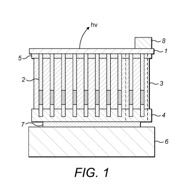
The figures are not to scale. Figure 1 shows a possible flip chip design. In
use therefore, light is emitted through the top of the device (marked ho).
Layer 1 is
the 13-Ga203 substrate.
Nanowires 2 are grown from substrate 1 epitaxially. Ideally, the 13-Ga203
substrate is n-type doped and the nanowires are formed from Al(In)GaN, AN or
GaN and are doped to create n-i-p or n-p junctions.
A filler 3 can be positioned between grown nanowires. A top electrode/light
reflecting layer 4 is positioned on top of nanowires 2. The light reflecting
layer may
also be provided with a p-electrode comprising Ni or Au. In use, this layer
reflects
any light emitted by the device to ensure that the light is emitted through
the top of
the device opposite the reflective layer. This is the so called flip-chip
arrangement
as the device is upside down compared to a conventional LED.
The n-electrode 8 is positioned on the substrate 1. That electrode might
comprise Ti, Al, Ni or/and Au. The substrate may be provided with a mask 5 to
allow growth of the nanowires in definitive positions on the substrate.
The whole device may be soldered to a submount 6 via solder layer 7.
When a forward current is passed vertically across the device, visible or UV
light, dependent on composition of matter, is generated in the nanowires and
is
emitted, possibly after reflecting off the reflective layer out the top of the
device.
When a reverse current is passed across the device and when the device is
exposed to visible or UV light, the nanowires absorb the visible or UV light,
CA 03059508 2019-10-09
WO 2018/189205 PCT/EP2018/059205
- 29 -
dependent on composition of matter, and converts it into current, working as a
photodetector.
Figure 2 shows a potential nanowire of the invention. The nanowire is
provided with different components in an axial direction by variation of the
elements
being supplied during the growing phase. Initially, an n-type doped GaN
material is
deposited on the n-type doped13-Ga203 substrate, followed by n-A1N or n-
(A1)GaN.
In the central section of the nanowire as shown are a series of multiple
quantum
wells formed from (In)(A1)GaN. There follows the p-type doped region based on
GaN, AlGaN or (A1)GaN, and an electron blocking layer based on p-Al(Ga)N and
finally a highly doped p-GaN layer for ohmic contacting to a p-electrode.
Figure 3 shows an alternative chip design in which the nanowires are grown
radially creating core shell structures. In use therefore, light is emitted
through the
top of the device (marked ho).
Layer 1 is the 13-Ga203 substrate. Nanowires 2 are grown from substrate layer
1 epitaxially. Ideally, 13-Ga203 substrate is n-type doped and the nanowires
formed
from Al(In)GaN, AN or GaN and are doped to create n-i-p or n-p junctions. The
substrate 1 can be provided with a mask layer 5.
A filler 3 can be positioned between grown nanowires. A top electrode/light
reflecting layer 4 is positioned on top of nanowires 2. The light reflecting
layer
may also be provided with a p-electrode comprising Ni or/and Au. In use, this
layer
reflects any light emitted by the device to ensure that the light is emitted
through the
top of the device opposite the reflective layer. This is the so called flip
chip
arrangement as the device is upside down compared to a conventional LED.
An n-electrode 8 is positioned on the n-doped substrate 1. When a forward
current is passed vertically across the device, visible or UV light, dependent
on
composition of matter, is generated in the nanowires and is emitted, possibly
after
reflecting off the reflective layer out the top of the device.
The whole device may be soldered to a submount 6 via solder layer 7.
When a reverse current is passed across the device and when the device is
exposed to visible or UV light, the nanowires absorb the visible or UV light,
dependent on composition of matter, and converts it into current, working as a
photodetector.
CA 03059508 2019-10-09
WO 2018/189205
PCT/EP2018/059205
- 30 -
Figure 4 shows a nanowire grown radially but having the same components
as those of figure 2 in a shell arrangement. The nanowire is provided with
different
components in a radial direction by variation of the elements being supplied
during
the growing phase. Initially, an n-type doped GaN core material is deposited,
followed by n-A1N or n-(A1)GaN. In the central shell of the nanowire as shown
are
a series of multiple quantum wells formed from (In)(A1)GaN. There follows the
p-
type doped region based on Al(Ga)N, and an electron blocking shell based on p-
Al(Ga)N and finally a highly doped p-GaN shell for ohmic contacting of the p-
electrode.
Figure 5 shows the fl-Ga203 unit cell with the (100), (-201), and (010),
crystallographic planes shown in red, blue, and green, respectively. Oxygen
atoms
are shown in red and Ga atoms in green.
Figure 6 show the fl-Ga203 unit cell with the (-201) and (010)
crystallographic planes as well as some physical properties of the 13-Ga203
substrate.
Oxygen atoms are shown in red and Ga atoms in green.
Fig. 7 shows the examples of (Al, In)GaN nanowires grown in the [0001]
direction on a 13-Ga203 substrate with (-201) surface orientation. Due to the
very
small lattice mismatch between13-Ga203 and (A1)GaN, i.e. [-201]/[0001], high-
quality vertical (Al, In)GaN nanowires can be epitaxially grown on the (-201)
surface of the 13-Ga203 substrate. For specific applications, solar-blind
photodetectors can be made from p-type (Al, In)GaN nanowires/n-type13-Ga203
substrate and LEDs can be fabricated from n-i-p (Al, In)GaN nanowires on top
of
the n-type 13-Ga203 substrate.
The (Al, In)GaN nanowires can be directly grown on top of13-Ga203 with (-
201) surface orientation without (Fig. 7 (a)) or with (Fig. 7 (b)) a thin
epitaxial III-V
buffer layer. The buffer layer can be made of, e.g. (Al, In)GaN, as shown in
figure 7
(b).
Figure 7 (c), shows the scanning electron microscopy (SEM) image of
vertical n-type doped GaN nanowires grown on top of a (-201)13-Ga203 substrate
with an n-type doped GaN buffer layer. The GaN nanowires and GaN buffer layer
were grown with nitrogen plasma-assisted MBE as described in the Experimental
Procedure section.
CA 03059508 2019-10-09
WO 2018/189205 PCT/EP2018/059205
- 31 -
Figure 8 (a) and (c), show p-type (Al, In)GaN nanowires epitaxially grown
on an n-type 13-Ga203 substrate without (a) and with (c) a p-type epitaxial
(Al,
In)GaN buffer layer, respectively. This forms p-n junctions between the n-
doped
Ga203 substrate and p-type (Al, In)GaN nanowires, which can be used as
material
for solar-blind photodiode detector.
In figure 8 (b) and (d), n-i-p doped (Al, In)GaN nanowires are epitaxially
grown on n-type13-Ga203 substrates without (b) and with (d) an epitaxial n-
type (Al,
In)GaN buffer layer, respectively. The Ga203 substrate can here e.g. act as a
transparent (for photons with an energy up to the Ga203 bandgap ¨4.8 eV) and
conductive electrode for vertical current injection (Al, In)GaN nanowire LEDs.
Example 1
N-type doped GaN nanowires have been grown on the (-201) plane of an n-doped 0-
Ga203 substrate under N-rich conditions in a Veeco GEN 930 molecular beam
epitaxy system with a radio-frequency nitrogen plasma source (PA-MBE, equipped
with an isolation gate valve). Prior to loading to the growth chamber, the
substrate is
thermally cleaned at 500 C for 1 hour in a preparation chamber. An n-type
doped
GaN buffer layer was grown at 550 C with Ga flux of 0.1 ML/s and N2 flow of
2.5
sccm at 495 W for 60 min. The buffer growth was initiated by opening the Ga
shutter and N2 gate valve and shutter simultaneously. After the successful
growth of
the buffer layer, the substrate temperature was ramped up to 765 C. The
nanowire
growth was then initiated by opening the Ga shutter and N2 gate valve and
shutter
simultaneously, and nanowire growth proceeded under a Ga flux of 0.5 ML/s and
N2
flow of 2.5 sccm at 495 W for 4 hours. The GaN buffer layer and nanowires are
n-
type doped with Si using a Si cell temperature of 1100 C.
Example 2
N-doped GaN nanowires are grown on the (-201) plane of an n-doped 13-Ga203
substrate using PA-MBE under N-rich conditions. A standard Knudsen effusion
cell
is used to supply Ga and Si atoms, while atomic nitrogen is generated from a
radio-
frequency plasma source that operates at 450 W. Prior to loading to the growth
CA 03059508 2019-10-09
WO 2018/189205 PCT/EP2018/059205
- 32 -
chamber, the substrate is thermally cleaned at 350 C for 1 hour in a
preparation
chamber. Catalyst-free, self-assembled n-doped GaN nanowires are then grown
directly on the n-doped 13-Ga203 substrate, without any intermediate buffer
layer.
The growth process is initiated by opening the Ga and N2 shutters
simultaneously,
i.e. no intentional nitridation takes place on the surface of the substrate.
The GaN
nanowires are n-type doped with Si using a cell temperature of 800 C and a
growth
time of 90 minutes.