Note: Descriptions are shown in the official language in which they were submitted.
MULTI-EMBEDDED RADIO FREQUENCY BOARD AND MOBILE DEVICE
INCLUDING THE SAME
BACKGROUND
1. Field
The exemplary embodiments generally relate to printed circuit boards and in
particular to
multi-embedded radio frequency boards and devices incorporating the same multi-
embedded
radio frequency boards.
2. Brief Description of Related Developments
Generally, to increase processing and other capabilities of printed circuit
boards, surface
mount components are coupled to both the front and back sides of the printed
circuit boards.
However, each printed circuit board has a finite size (e.g., surface area to
which the surface
mount components may be coupled). With respect to communications, such as
through
antenna arrays, phased array antennas may have a high element count such as
when the
antenna elements are spaced apart by a distance that is less than the
wavelength of the
frequency being transmitted or received (e.g., a sub-frequency or wavelength
spacing). This
close packed lattice of antenna elements forces the surface mount components
to be highly
integrated and are typically packaged as a radio frequency integrated circuit
(RFIC), and the
degree of signal processing is therefore performance limited to what can be
packed on the
surface mount parts within the finite surface area of the printed circuit
board.
In other aspects, multiple circuit boards are coupled to each other using
cables, such as
between radio frequency modules and antenna arrays. The use of cables works
well when the
number of interconnects are low; however, where the number of interconnects
are high (such
1
CA 3059703 2019-10-23
as with high antenna element count phased arrays with sub-frequency spacing),
the use of
cable becomes impractical and increases the area needed to house the circuit
boards.
SUMMARY
The following is a non-exhaustive list of examples, which may or may not be
claimed, of the
subject matter according to the present disclosure.
One example of the subject matter according to the present disclosure relates
to a multi-
embedded radio frequency board comprising: at least one radio frequency signal
generating
printed circuit board; at least one embedded radio frequency module printed
circuit board
communicably coupled to the at least one radio frequency signal generating
printed circuit
board; and at least one communication printed circuit board communicably
coupled to one or
more of the at least one radio frequency signal generating printed circuit
board or the at least
one embedded radio frequency module printed circuit board; wherein the at
least one radio
frequency signal generating printed circuit board, the at least one embedded
radio frequency
module printed circuit board, and the at least one communication printed
circuit board are
stacked one board on top of the others, and adjacent boards of the at least
one radio frequency
signal generating printed circuit board, the at least one embedded radio
frequency module
printed circuit board, and the at least one communication printed circuit
board are coupled by
a respective interconnection join layer so as to form an integrated printed
circuit board
module.
Another example of the subject matter according to the present disclosure
relates to a multi-
embedded radio frequency board comprising: a plurality of printed circuit
boards stacked one
on the others, at least one of the printed circuit boards of the plurality of
printed circuit boards
being configured so as to have a different processing function than another
processing
function of another printed circuit board of the plurality of printed circuit
boards; and an
2
CA 3059703 2019-10-23
interconnection join layer disposed between adjacent printed circuit boards of
the plurality of
printed circuit boards so as to physically and electrically couple the
adjacent printed circuit
boards to each other so as to form an integrated printed circuit board module
having a
predetermined radio frequency communication characteristic.
Still another example of the subject matter according to the present
disclosure relates to a
mobile device including a multi-embedded radio frequency board, comprising: a
frame; and
the multi-embedded radio frequency board being coupled to the frame, the multi-
embedded
radio frequency board including a plurality of printed circuit boards stacked
one on the other,
at least one of the printed circuit boards of the plurality of printed circuit
boards being
configured so as to have a different processing function than another
processing function of
another printed circuit board of the plurality of printed circuit boards; and
an interconnection
join layer disposed between adjacent printed circuit boards of the plurality
of printed circuit
boards so as to physically and electrically couple the adjacent printed
circuit boards to each
other so as to form an integrated printed circuit board module having a
predetermined radio
frequency communication characteristic.
Further still another example of the subject matter according to the present
disclosure relates
to a radio frequency signal repeater comprising: a first communication printed
circuit board; a
second communication printed circuit board; at least one embedded radio
frequency module
printed circuit board disposed between and communicably coupled to both the
first
communication printed circuit board and the second communication printed
circuit board;
and wherein the at least one embedded radio frequency module printed circuit
board, the first
communication printed circuit board, and the second communication printed
circuit board are
stacked one board on top of the others, and adjacent boards of the at least
one embedded
radio frequency module printed circuit board, the first communication printed
circuit board,
3
CA 3059703 2019-10-23
and the second communication printed circuit board are coupled by a respective
interconnection join layer so as to form an integrated printed circuit board
module.
Yet another example of the subject matter according to the present disclosure
relates to a radio
frequency signal lens comprising: a first communication printed circuit board;
a second
communication printed circuit board; at least one embedded radio frequency
module printed
circuit board disposed between and communicably coupled to both the first
communication
printed circuit board and the second communication printed circuit board; and
wherein the at
least one embedded radio frequency module printed circuit board, the first
communication
printed circuit board, and the second communication printed circuit board are
stacked one
board on top of the others, and adjacent boards of the at least one embedded
radio frequency
module printed circuit board, the first communication printed circuit board,
and the second
communication printed circuit board are coupled by a respective
interconnection join layer so
as to form an integrated printed circuit board module.
Yet another example of the subject matter according to the present disclosure
relates to a multi-
embedded radio frequency board comprising: a plurality of printed circuit
boards, at least one
of the printed circuit boards of the plurality of printed circuit boards being
configured so as to
have a different processing function than another processing function of
another printed circuit
board of the plurality of printed circuit boards; and an interconnection join
layer disposed
between adjacent printed circuit boards of the plurality of printed circuit
boards so as to
physically and electrically couple the adjacent printed circuit boards to each
other so as to form
an integrated printed circuit board module having a predeteimined radio
frequency
communication characteristic, wherein the plurality of printed circuit boards
form a stack of
printed circuit boards having a first end and a second end, the first end
being formed at least
in part by a surface of a first end printed circuit board and the second end
being foimed
4
Date recue/Date received 2023-04-10
at least in part by a surface of a second end printed circuit board, and
wherein at least one of
the first end printed circuit board and the second end printed circuit board
comprises a radio
frequency signal output printed circuit board including an array of antenna
horns coupled
thereto and founing a phased array antenna.
Yet another example of the subject matter according to the present disclosure
relates to a multi-
embedded radio frequency board comprising: at least one radio frequency signal
generating
printed circuit board; at least one embedded radio frequency module printed
circuit board
communicably coupled to the at least one radio frequency signal generating
printed circuit
board; and at least one communication printed circuit board communicably
coupled to one or
more of the at least one radio frequency signal generating printed circuit
board and the at least
one embedded radio frequency module printed circuit board, wherein adjacent
boards of the at
least one radio frequency signal generating printed circuit board, the at
least one embedded
radio frequency module printed circuit board, and the at least one
communication printed
circuit board are coupled by a respective interconnection join layer so as to
foini an integrated
printed circuit board module, wherein the at least one radio frequency signal
generating printed
circuit board, the at least one embedded radio frequency module printed
circuit board, and the
at least one communication printed circuit board form a stack of printed
circuit boards having
a first end fonned at least in part by a surface of the at least one radio
frequency signal
generating printed circuit board and a second end formed at least in part by a
surface of the at
least one communication printed circuit board, and wherein the at least one
communication
printed circuit board comprises a radio frequency signal output printed
circuit board including
an array of antenna horns coupled thereto and forming a phased array antenna.
4a
Date recue/Date received 2023-04-10
Yet another example of the subject matter according to the present disclosure
relates to a radio
frequency signal repeater comprising: a first communication printed circuit
board; a second
communication printed circuit board; and at least one embedded radio frequency
module
printed circuit board disposed between and communicably coupled to both the
first
communication printed circuit board and the second communication printed
circuit board,
wherein the at least one embedded radio frequency module printed circuit
board, the first
communication printed circuit board, and the second communication printed
circuit board are
stacked one board on top of the others, and adjacent boards of the at least
one embedded radio
frequency module printed circuit board, the first communication printed
circuit board, and the
second communication printed circuit board are coupled by a respective
interconnection join
layer so as to form an integrated printed circuit board module, and wherein
one of the first
communication printed circuit board and the second communication printed
circuit board
comprises a radio frequency signal output printed circuit board including an
array of antenna
horns coupled thereto and forming a phased array antenna.
Yet another example of the subject matter according to the present disclosure
relates to a radio
frequency signal lens comprising: a first communication printed circuit board;
a second
communication printed circuit board; and at least one embedded radio frequency
module
printed circuit board disposed between and communicably coupled to both the
first
communication printed circuit board and the second communication printed
circuit board,
wherein the at least one embedded radio frequency module printed circuit
board, the first
communication printed circuit board, and the second communication printed
circuit board are
stacked one board on top of the others, and adjacent boards of the at least
one embedded radio
frequency module printed circuit board, the first communication printed
circuit board, and the
second communication printed circuit board are coupled by a respective
interconnection join
layer so as to form an integrated printed circuit board module, and wherein
one of the first
4b
Date recue/Date received 2023-04-10
communication printed circuit board and the second communication printed
circuit board
comprises a radio frequency signal output printed circuit board including an
array of antenna
horns coupled thereto and forming a phased array antenna.
BRIEF DESCRIPTION OF THE DRAWINGS
Having thus described examples of the present disclosure in general teuns,
reference will now
be made to the accompanying drawings, which are not necessarily drawn to
scale, and wherein
like references characters designate the same or similar parts throughout the
several views, and
wherein:
Figs. 1A and 1B (collectively referred to herein as Fig. 1) are a schematic
block diagram of a
multi-embedded radio frequency board in accordance with aspects of the present
disclosure;
Fig. 2 is a schematic block diagram of a mobile device including a multi-
embedded radio
frequency board in accordance with aspects of the present disclosure;
4c
Date recue/Date received 2023-04-10
Fig. 3 is a schematic block diagram of a radio frequency signal repeater
including a multi-
embedded radio frequency board in accordance with aspects of the present
disclosure;
Fig. 4 is a schematic block diagram of a radio frequency signal lens including
a multi-
embedded radio frequency board in accordance with aspects of the present
disclosure;
Fig. 5 is an exemplary schematic diagram of a multi-embedded radio frequency
board in
accordance with aspects of the present disclosure;
Fig. 6 is an exemplary schematic diagram of a multi-embedded radio frequency
board in
accordance with aspects of the present disclosure;
Fig. 7 is an exemplary schematic diagram of a multi-embedded radio frequency
board in
accordance with aspects of the present disclosure;
Fig. 8 is an exemplary schematic diagram of a multi-embedded radio frequency
board in
accordance with aspects of the present disclosure;
Fig. 9 is an exemplary schematic diagram of a multi-embedded radio frequency
board in the
form of a radio frequency receiver in accordance with aspects of the present
disclosure;
Fig. 10 is an exemplary schematic diagram of an antenna array of a multi-
embedded radio
frequency board in accordance with aspects of the present disclosure;
Fig. 11 is an exemplary schematic cross-sectional diagram of a portion of a
multi-embedded
radio frequency board in accordance with aspects of the present disclosure;
Fig. 12 is an exemplary schematic diagram the radio frequency signal repeater
of Fig. 3 in
accordance with aspects of the present disclosure;
CA 3059703 2019-10-23
Fig. 13 is an exemplary schematic diagram the radio frequency signal lens of
Fig. 4 in
accordance with aspects of the present disclosure; and
Figs. 14A and 14B are exemplary schematic illustrations respectively of the
mobile device of
Fig. 2 and a portion thereof.
DETAILED DESCRIPTION
Illustrative, non-exhaustive examples, which may or may not be claimed, of the
subject
matter according to the present disclosure are provided below. It is noted
that the expression
"radio frequency" may be referred to in this text and drawings by the acronym
"RF".
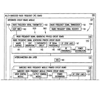
Referring to Fig. 1, the aspects of the present disclosure provide for a multi-
embedded radio
frequency board 100 having an integrated circuit board module 101 that
combines embedded
radio frequency module printed circuit board(s) 120 with radio frequency
signal generating
printed circuit board(s) 140 and communication printed circuit board(s) 130 in
a single
integrated assembly. The multi-embedded radio frequency board 100 provides an
increased
surface area for mounting surface mount components or printed components (such
as
antennas) where the increase in surface area is effected through embedding
components
within the multi-embedded radio frequency board 100. For example, the
integrated circuit
board module 101 having multiple circuit boards stacked one board on top of
the other boards
so that components that would otherwise occupy the surface area of the multi-
embedded
radio frequency board 100 can be embedded within the circuit boards of the
stack of printed
circuit boards 104. The increased surface area provides for a larger array of
antenna horns
110 to be coupled to the multi-embedded radio frequency board 100. The aspects
of the
present disclosure also provide increased capabilities (e.g., signal
generation, signal
processing, signal transmission, signal reception, signal routing, power
routing, etc. as
described herein) within the integrated circuit board module 101 of the multi-
embedded radio
6
CA 3059703 2019-10-23
frequency board 100. The integrated circuit board module 101 includes multiple
circuit
boards stacked one board on top of the other boards where adjacent circuit
boards are coupled
to each other by a respective interconnection join layer 102 that provides for
the
interconnection (e.g., radio frequency, power, control signals, etc.) and
coupling of adjacent
circuit boards through vias 103.
The stacked interconnection and coupling of the adjacent circuit boards of the
integrated
circuit board module 101 mitigate radio frequency signal loss that would
otherwise occur as a
result of transmission of the radio frequency signal through cables and would
otherwise
directly translate into a radio frequency power loss for a transmitter or a
degradation to noise
for a receiver. For example, an embedded radio frequency processing component
(such as
those described herein) may be placed substantially directly at feeds 111 of
the array of
antenna horns 110 in accordance with the aspects of the present disclosure.
The aspects of the present disclosure substantially eliminate human error in
the assembly of
the multi-embedded radio frequency board 100 and provide for low-cost-highly
repeatable,
and high performance phased array antenna systems, radio frequency repeater
systems,
and/or radio frequency lens systems. For example, any embedded components are
disposed
within a respective circuit board as that circuit board is formed and
inspected in an automated
machine process. Any surface mount components of the multi-embedded radio
frequency
board 100 are also coupled to the multi-embedded radio frequency board 100 and
inspected
in an automated machine process. Humans merely move subassemblies of the multi-
embedded radio frequency board 100 from one automated machine process to
another
automated machine process.
7
CA 3059703 2019-10-23
The multi-embedded radio frequency board 100, in accordance with the aspects
of the present
disclosure, may be employed in receive and/or transmit phased array
communications
terminals. For example, the multi-embedded radio frequency board 100 of the
present
disclosure may be used to facilitate, as non-limiting examples, air-to-space
communications,
air-to-ground communications, air-to-air communications, ground-to-space
communications,
ground-to-ground communications, mobile-to-mobile space-to-ground
communications, and
space-to-space communications. The multi-embedded radio frequency board 100,
in
accordance with aspects of the present disclosure, may also be employed to
receive and/or
transmit actively scanned radars in, as non-limiting examples, airborne, land-
based, sea, and
space applications. The multi-embedded radio frequency board 100 may also be
employed as
a radio frequency signal repeater 300 (Fig. 3) or a radio frequency signal
lens 400 (Fig. 4).
The multi-embedded radio frequency board 100 may also provide for a steerable
antenna for
mobile applications (such as in a mobile device 200 (Fig. 2)). The aspects of
the present
disclosure may operate in any suitable frequency range(s) including, but not
limited to,
microwave frequency, millimeter frequencies, and 5G applications (and above).
Referring to Figs. 1 and 5, the multi-embedded radio frequency board 100
includes a plurality
of printed circuit boards 105 stacked one on the others so as to form stack of
printed circuit
boards 104. At least one of the printed circuit boards of the plurality of
printed circuit boards
105 is configured so as to have a different processing function than another
processing
function of another printed circuit board of the plurality of printed circuit
boards 105. For
example, the different processing function comprises one or more of radio
frequency signal
generation, radio frequency transmission, radio frequency reception, heat
dissipation, power
distribution, radio frequency signal processing (e.g., amplification,
conditioning), radio
frequency transitions, and radio frequency signal routing. The another
processing function
(i.e., the different processing function) comprises a different one or more of
radio frequency
8
CA 3059703 2019-10-23
signal generation, radio frequency transmission, radio frequency reception,
heat dissipation,
power distribution, radio frequency signal processing (e.g., amplification,
conditioning),
radio frequency transitions, and radio frequency signal routing. In other
aspects, two or more
of the printed circuit boards of the plurality of printed circuit boards may
have the same or a
common processing function.
The plurality of printed circuit boards 105 includes at least one radio
frequency signal
generating printed circuit board 140, at least one embedded radio frequency
module printed
circuit board 120 communicably coupled to the at least one radio frequency
signal generating
printed circuit board 140, and at least one communication printed circuit
board 130
communicably coupled to one or more of the at least one radio frequency signal
generating
printed circuit board 140 and/or the at least one embedded radio frequency
module printed
circuit board 120. The at least one radio frequency signal generating printed
circuit board
140, the at least one embedded radio frequency module printed circuit board
120, and the at
least one communication printed circuit board 130 are stacked one board on top
of the others
so as to form the stack of printed circuit boards 104. Adjacent boards of the
at least one radio
frequency signal generating printed circuit board 140, the at least one
embedded radio
frequency module printed circuit board 120, and the at least one communication
printed
circuit board 130 are coupled by a respective interconnection join layer 102
so as to form the
integrated printed circuit board module 101. The interconnection join layer
102 is disposed
between adjacent printed circuit boards of the plurality of printed circuit
boards 105 so as to
physically and electrically couple the adjacent printed circuit boards to each
other so as to
form the integrated printed circuit board module 101 having the predetermined
radio
frequency communication characteristic. The predetermined radio frequency
communication
characteristic may be one or more of radio frequency signal reception and
transmission, radio
frequency lensing, and radio frequency repetition.
9
CA 3059703 2019-10-23
The integrated printed circuit board module 101 and the interconnection join
layers 102
thereof may provide for substantially lossless radio frequency signal
couplings, substantially
lossless power couplings, and substantially lossless control signal couplings
between the
adjacent boards. The stack of printed circuit boards 104 includes a first end
500 formed at
least in part by a major surface 141 of at least one of the first end printed
circuit board 560
(Fig. 5) (e.g., such as for example, the at least one radio frequency signal
generating printed
circuit board 140) and a second end 501 formed at least in part by a major
surface 134 of at
least one second end printed circuit board 561 (e.g., such as for example, the
at least one
communication printed circuit board 130). In one aspect, at least one of the
first end printed
circuit board 560 and the second end printed circuit board 561 (Fig. 5)
comprises a radio
frequency signal output printed circuit board 131 (Fig. 1). In one aspect, at
least one of the
first end printed circuit board 560 and the second end printed circuit board
561 comprises a
radio frequency signal input printed circuit board 132 (Fig. 1). In another
aspect, at least one
of the first end printed circuit board 560 and the second end printed circuit
board 561
comprises a radio frequency signal transceiver printed circuit board 133.
While the at least
one radio frequency signal generating printed circuit board 140 may be
referred to as the first
end printed circuit board and the at least one communication printed circuit
board 130 may be
referred to as the second end printed circuit board 561 in some aspects, in
other aspects of the
present disclosure each of the first end 500 and the second end 501 may
include a
communication printed circuit board 130.
Referring to Figs. 1, 5, and 10, the integrated printed circuit board module
101 is configured
as a radio frequency signal transmitter 152. For example, the at least one
communication
printed circuit board 130 comprises a radio frequency signal output printed
circuit board 131.
In one aspect, the radio frequency signal output printed circuit board 131
includes an array of
antenna horns 110 coupled thereto. In one aspect, the array of antenna horns
110 have a sub-
CA 3059703 2019-10-23
frequency spacing, while in other aspects, the array of antenna horns 110 have
a spacing that
is a multiple of a frequency wavelength output by the radio frequency signal
output printed
circuit board 131. The array of antenna horns 110 may form a phased array
antenna 1010
(Fig. 10). The array of antenna horns 110 include two or more antennas 1000
printed on the
major surface 134 of the at least one communication printed circuit board 130;
while in other
aspects a single antenna 1000 may be printed on the major surface 134. In
another aspect, the
radio frequency signal output printed circuit board 131 includes a radio
frequency connector
112 in addition to or in lieu of the array of antenna horns 110. The radio
frequency connector
112 may provide for wired signal transmission from the radio frequency signal
output printed
circuit board 131.
In another aspect, the integrated printed circuit board module 101 is
configured as a radio
frequency signal receiver 151. For example, the at least one communication
printed circuit
board 130 (which may be one of the first end printed circuit board 560 (Fig.
5) and the
second end printed circuit board 561 (Fig. 5)) includes a radio frequency
signal input printed
circuit board 132. The radio frequency signal input printed circuit board 132
includes an
array of antenna horns 110 coupled thereto. In one aspect, the radio frequency
signal input
printed circuit board 132 includes at least one integrated circuit 177
configured to receive a
radio frequency signal; while in other aspects the radio frequency signal may
be received by
an integrated circuit within any one of the boards in the stack of printed
circuit boards 104.
In one aspect, the array of antenna horns 110 have a sub-frequency spacing,
while in other
aspects, the array of antenna horns 110 have a spacing that is a multiple of a
frequency
wavelength input to the radio frequency signal input printed circuit board
132. The array of
antenna horns 110 may form a phased array antenna 1010 (Fig. 10). The array of
antenna
horns 110 include two or more antennas 1000 printed on the major surface 134
of the at least
one communication printed circuit board 130; while in other aspects a single
antenna 1000
11
CA 3059703 2019-10-23
may be printed on the major surface 134. In another aspect, the radio
frequency signal input
printed circuit board 132 includes a radio frequency connector 112 in addition
to or in lieu of
the array of antenna horns 110. The radio frequency connector 112 may provide
for wired
signal transmission to the radio frequency signal input printed circuit board
132.
In still another aspect, the integrated printed circuit board module 101 is
configured as a radio
frequency signal transceiver 150. For example, the at least one communication
printed
circuit board 130 comprises a radio frequency signal transceiver printed
circuit board 133. In
one aspect, the radio frequency signal transceiver printed circuit board 133
includes an array
of antenna horns 110 coupled thereto. In one aspect, the array of antenna
horns 110 have a
sub-frequency spacing, while in other aspects, the array of antenna horns 110
have a spacing
that is a multiple of a frequency wavelength input to the radio frequency
signal input printed
circuit board 132. The array of antenna horns 110 may form a phased array
antenna 1010
(Fig. 10). The array of antenna horns 110 include two or more antennas 1000
printed on the
major surface 134 of the at least one communication printed circuit board 130;
while in other
aspects a single antenna 1000 may be printed on the major surface 134. In
another aspect, the
radio frequency signal transceiver printed circuit board 133 includes a radio
frequency
connector 112 in addition to or in lieu of the array of antenna horns 110. The
radio frequency
connector 112 may provide for wired signal transmission to and from the radio
frequency
signal transceiver printed circuit board 133.
The at least one communication printed circuit board 130 includes radio
frequency strip lines
137 configured to route radio frequency signals to and from adjacent printed
circuit boards
(such as to one or more of the at least one embedded radio frequency module
printed circuit
board 120 and the at least one radio frequency signal generating printed
circuit board 140).
In one aspect, the at least one communication printed circuit board 130
includes heat
12
CA 3059703 2019-10-23
dissipation 139, such as conductive traces coupled to any suitable heat sink
161 coupled to
the at least one communication printed circuit board 130.
Referring to Figs. 1 and 5, the at least one radio frequency signal generating
printed circuit
board 140 (which is may be one of the first end printed circuit board 560
(Fig. 5) and the
second end printed circuit board 561 (Fig. 5)) includes at least one
integrated circuit 142
configured to generate a radio frequency signal. The integrated circuit 142
may be surface
mounted to the major surface 141 of the at least one radio frequency signal
generating printed
circuit board 140 or the integrated circuit may be embedded within the at
least one radio
frequency signal generating printed circuit board 140. The at least one radio
frequency signal
generating printed circuit board 140 includes one or more of heat dissipation
143 (such as
conductive traces coupled to any suitable heat sink 160 coupled to the at
least one radio
frequency signal generating printed circuit board 140), power distribution
144, radio
frequency signal processing 145 (e.g., amplification, conditioning), and radio
frequency
transitions 146. The at least one radio frequency signal generating printed
circuit board 140
includes radio frequency strip lines 147 configured to route radio frequency
signals to and
from adjacent printed circuit boards (such as to one or more of the at least
one embedded
radio frequency module printed circuit board 120 and the at least one
communication printed
circuit board 130).
Referring to Figs. 1 and 5, the at least one embedded radio frequency module
printed circuit
board 120 is disposed between the at least one radio frequency signal
generating printed
circuit board 140 and the at least one communication printed circuit board
130. The a least
one embedded radio frequency module printed circuit board 120 forms at least
one
intermediate printed circuit board 510 (see Fig. 5) disposed in the stack of
printed circuit
boards 104 between a first end printed circuit board 560 (such as in one
aspect, e.g., the at
13
CA 3059703 2019-10-23
least one radio frequency signal generating printed circuit board 140) and a
second end
printed circuit board 561 (such as in one aspect, e.g., the at least one
communication printed
circuit board 130). As an intermediate printed circuit board 510, the at least
one embedded
radio frequency module printed circuit board 120 includes radio frequency
strip lines 121
configured to route radio frequency signals at least between adjacent printed
circuit boards.
The at least one embedded radio frequency module printed circuit board 120
includes power
distribution 122 routing to one or more adjacent printed circuit boards. The
at least one
embedded radio frequency module printed circuit board 120 includes one or more
of an input
control module 123 and output control module 124 embedded within the at least
one
embedded radio frequency module printed circuit board 120, where the input
control module
123 and output control module 124 may send control signals to the integrated
circuits 142 of
the at least one radio frequency signal generating printed circuit board 140
or other suitable
modules (e.g., power distribution modules, signal processing modules, etc.)
embedded in one
or more of the at least one embedded radio frequency module printed circuit
board 120, the at
least one of the radio frequency signal generating printed circuit board 140,
and the at least
one communication printed circuit board 130.
Referring to Figs. 1, 5 and 11, in one aspect, the at least one embedded radio
frequency
module printed circuit board 120 includes a radio frequency signal processing
device 125
embedded within the at least one embedded radio frequency module printed
circuit board
120. The a radio frequency signal processing device 125 may be substantially
similar to a
radio frequency signal processing device 148 that effects radio frequency
signal processing
145 in the at least one radio frequency signal generating printed circuit
board 140. The radio
frequency signal processing device 125 is an integrated circuit 126, a radio
frequency signal
amplifier 127, a radio frequency signal conditioner 128, or a combination
thereof.
14
CA 3059703 2019-10-23
Referring to Figs. 1, 5, and 11, the at least one embedded radio frequency
module printed
circuit board comprises radio frequency strip lines 121 configured to route
radio frequency
signals at least between adjacent printed circuit boards of the stack of
printed circuit boards
104. The at least one embedded radio frequency module printed circuit board
120 also
includes power distribution 122 routing to one or more adjacent printed
circuit boards of the
stack of printed circuit boards 104. In one aspect, the power distribution 122
of the at least
one embedded radio frequency module printed circuit board 120 may include at
least one
capacitor 1100 (Fig. 11) embedded within the at least one embedded radio
frequency module
printed circuit board 120; while in other aspects any suitable power source
may be provided.
The at least one embedded radio frequency module printed circuit board 120 may
include at
least one direct current filtering device 129 embedded within the at least one
intermediate
printed circuit board 510 (see Fig. 5). In one aspect, the at least one direct
current filtering
device 129 may be part of the power distribution 122, while in other aspects,
the at least one
direct current filtering device 129 may be coupled to the power distribution
122 in any
suitable manner. The at least one direct current filtering device 129 may
provide regulated
power to one or more of the embedded modules described herein. Fig. 11 is
illustrative of the
manner in which embedded modules are embedded into the one or more of the at
least one
embedded radio frequency module printed circuit board 120. Fig. 11 is also
illustrative of the
radio frequency strip lines 121, radio frequency transitions 146, and power
distribution 122 of
the embedded radio frequency module printed circuit board 120.
In some aspects of the present disclosure one or more of the at least one
radio frequency
signal generating printed circuit board 140 and the at least one communication
printed circuit
board 130 include embedded modules, such as those described herein and with
respect to the
at least one embedded radio frequency module printed circuit board 120. As
such, in these
aspects Fig. 11 is also illustrative of the manner in which the embedded
modules are
CA 3059703 2019-10-23
embedded into the one or more of the at least one radio frequency signal
generating printed
circuit board 140 and the at least one communication printed circuit board
130. Fig. 11 is
also illustrative of the radio frequency strip lines 137, 147, radio frequency
transitions 146,
and power distribution 138, 144 (which are substantially similar to the radio
frequency strip
lines 121 and power distribution 122) of the at least one radio frequency
signal generating
printed circuit board 140 and the at least one communication printed circuit
board 130.
Referring to Figs. 1 and 6-8 the multi-embedded radio frequency board 100 may
include any
suitable number of printed circuit boards within the stack of printed circuit
boards 104, where
each board is coupled to an adjacent board by a respective interconnection
join layer. For
example, Fig. 6 illustrates an example where the multi-embedded radio
frequency board 100
includes three printed circuit boards, e.g., a radio frequency signal
generating printed circuit
board 140 (disposed at either the first end 500 or the second end 501), an
embedded radio
frequency module printed circuit board 120, and a communication printed
circuit board
(disposed at the other of the first end 500 or the second end 501).
Fig. 7 illustrates an example where the multi-embedded radio frequency board
100 includes
four printed circuit boards, e.g., a radio frequency signal generating printed
circuit board 140
(disposed at either the first end 500 or the second end 501), two embedded
radio frequency
module printed circuit boards 120, and a communication printed circuit board
(disposed at the
other of the first end 500 or the second end 501). In this example, each of
the embedded
radio frequency module printed circuit boards 120 may have radio frequency
signal
processing devices 125 performing one or more different functions.
Fig. 8 illustrates an example where the multi-embedded radio frequency board
100 includes
seven printed circuit boards, e.g., a radio frequency signal generating
printed circuit board
140 (disposed at either the first end 500 or the second end 501), five
embedded radio
16
CA 3059703 2019-10-23
frequency module printed circuit boards 120A-120E, and a communication printed
circuit
board (disposed at the other of the first end 500 or the second end 501). In
this example, each
of the embedded radio frequency module printed circuit boards 120 may have
radio
frequency signal processing devices 125 performing one or more different
functions. For
example, radio frequency module printed circuit boards 120A, 120C, 120E may
include one
or more radio frequency signal processing devices 125 and/or capacitors 1100.
Radio
frequency module printed circuit boards 120B, 120D may include radio frequency
strip lines
121, radio frequency transitions 146, power distribution 122, input control
module 123,
and/or output control module 124. In other aspect, each of the radio frequency
module
printed circuit boards 120A-120E may be suitably configured to perform alone
or in
combination with other boards of the radio frequency module printed circuit
boards 120A-
120E any suitable control and signal processing functions.
Referring to Figs. 1 and 9, an example of the multi-embedded radio frequency
board 100
including seven printed circuit boards is illustrated. In this example the
multi-embedded
radio frequency board 100 is configured as a radio frequency signal
transceiver 150;
however, in other aspects the multi-embedded radio frequency board 100 may be
configured
as the radio frequency signal transmitter 152 or the radio frequency signal
receiver 151. In
this example, the radio frequency signal generating printed circuit board 140
includes surface
mount (in other aspects could be embedded) radio frequency signal processing
components
(e.g., integrated circuits 142, radio frequency signal processing modules 145,
etc.) and a
power distribution 144 (including power source 144S). Embedded radio frequency
module
printed circuit board 120A is configured for radio frequency signal
conditioning and includes
any suitable radio frequency signal processing devices 125 such as one or more
radio
frequency signal conditioner 128 modules/integrated circuits coupled to the
radio frequency
signal processing components of the radio frequency signal generating printed
circuit board
17
CA 3059703 2019-10-23
140. The embedded radio frequency module printed circuit board 120B is
configured as a
radio frequency routing layer (e.g., radio frequency transitions 146 and radio
frequency strip
lines 121 that couple the embedded components of the adjacent embedded radio
frequency
module printed circuit boards 120A, 120C). The embedded radio frequency module
printed
circuit board 120B also includes power distribution 122 (e.g., for supplying
power to the
embedded modules of embedded radio frequency module printed circuit boards
120A, 120C).
Embedded radio frequency module printed circuit board 120C is configured as
another signal
conditioning layer (that performs different signal conditioning than that of
embedded radio
frequency module printed circuit board 120A) that includes any suitable radio
frequency
signal processing devices 125 such as one or more radio frequency signal
conditioner 128
modules/integrated circuits coupled to the radio frequency signal processing
components of
the embedded radio frequency module printed circuit boards 120A, 120E.
Embedded radio
frequency module printed circuit board 120D is configured as another radio
frequency
routing layer (e.g., radio frequency transitions 146 and radio frequency strip
lines 121 that
couple the embedded components of the adjacent embedded radio frequency module
printed
circuit boards 120C, 120E). The embedded radio frequency module printed
circuit board
120D also includes power distribution 122 (e.g., for supplying power to the
embedded
modules of embedded radio frequency module printed circuit board 120E).
Embedded radio
frequency module printed circuit board 120E is configured as an amplifier
layer and includes
one or more radio frequency signal amplifiers 127 and any other suitable radio
frequency
signal processing devices 125 that are coupled to feeds 1 1 1 of respective
antenna horns 900
of the array of antenna horns 110 of the communication printed circuit board
130 (which is
configured as the radio frequency input printed circuit board 132). As can be
seen in Fig. 9,
each of the embedded radio frequency module printed circuit board 120A, 120B,
120C,
120D, 120E is configured for a respective frequency processing function (e.g.,
different from
18
CA 3059703 2019-10-23
another function performed by another embedded radio frequency module printed
circuit
board in the stack of printed circuit boards 104).
Referring to Figs. 1 and 2, the multi-embedded radio frequency board 100 may
be included in
a mobile device 200 so as to perform radio frequency signal reception and/or
transmission.
The mobile device may be a handheld communication device 1400 (e.g., cellular
phone,
handheld radio, etc.), a spacecraft 201 (e.g., satellite, space shuttle, space
capsule, telescope,
etc.), an aircraft 202 (lighter than air vehicle, fixed wing aircraft,
variable wing aircraft, tilt-
rotor aircraft, rotary wing aircraft, etc.), a maritime vessel 203, or
terrestrial vehicle 204. The
mobile device 200 includes any suitable frame 210 to which the multi-embedded
radio
frequency board 100 is coupled. For exemplary purposes, referring also to
Figs. 14A and
14B, the mobile device is illustrated as a mobile/cellular phone where the
multi-embedded
radio frequency board 100 includes a radio frequency signal generating printed
circuit board
140, and embedded radio frequency module printed circuit board 120, and a
communication
printed circuit board 130. While the multi-embedded radio frequency board 100
includes a
stack of printed circuit boards 104 that includes three circuit boards, in
other aspects, the
stack of printed circuit boards 104 may include any suitable number of printed
circuit boards,
depending on, e.g., predetermined processing functions of the mobile device
200. The radio
frequency signal generating printed circuit board 140 (which as described
herein may be the
first end printed circuit board 560 or the second end printed circuit board
561) may be as
described herein and include any suitable integrated circuits 142 (or other
suitable processors)
and radio frequency signal processing 145 so as to configure the radio
frequency signal
generating printed circuit board 140 as a mobile communication device
processor printed
circuit board 1420 programmed to make, receive, and process cellular signals.
The
embedded radio frequency module printed circuit board 120 and the
communication printed
circuit board 130 may be as described herein, however in this aspect the
communication
19
CA 3059703 2019-10-23
printed circuit board 130 may be configured as a radio frequency signal
transceiver printed
circuit board 133 so as to send and receive cellular (or any other suitable
radio frequency
wavelength) signals 1410. In other aspects, the mobile device 200 may include
the radio
frequency signal input printed circuit board 132 and/or the radio frequency
output printed
circuit board 131 described above. In this aspect, the multi-embedded radio
frequency board
100 is coupled to the frame 210 so that the array of antenna horns 110 is
exposed (or if the
frame is radio frequency wave transparent the antenna horns may not be
exposed) so as to
transmit and receive the cellular signals 1410. In this aspect, the array of
antenna horns 110
is steerable, so as to point the array of antenna horns 110 to a particular
target, by rotating (or
otherwise changing an orientation) the handheld communication device 1400
(e.g., about one
or more axes of rotation X, Y, Z).
Where the mobile device comprises a spacecraft 201, an aircraft 202, or a
maritime vessel
203, the antenna array of the multi-embedded radio frequency board 100 coupled
thereto may
be pointed in a manner similar to that described above with respect to the
handheld
communication device 1400 (e.g., by changing an attitude/orientation of the
mobile device
200). In other aspects, the multi-embedded radio frequency board 100 may be
coupled to the
spacecraft 201, the aircraft 202, or the maritime vessel 203 with a gimballed
coupling so that
the multi-embedded radio frequency board 100 may be pointed in a predetermined
direction
independent of the attitude/orientation of the mobile device 200.
Referring to Figs. 1, 3, and 12, the aspects of the present disclosure may
provide for a radio
frequency signal repeater 300 that includes the multi-embedded radio frequency
board 100,
so as to perform radio frequency repetition. For example, the radio frequency
signal repeater
300 includes an integrated printed circuit board module 101 having a first
communication
printed circuit board 330, a second communication printed circuit board 331,
and at least one
CA 3059703 2019-10-23
embedded radio frequency module printed circuit board 120 disposed between and
communicably coupled to both the first communication printed circuit board 330
and the
second communication printed circuit board 331. The at least one embedded
radio frequency
module printed circuit board 120 may be as described herein. The first
communication
printed circuit board 330 and the second communication printed circuit board
331 may be
substantially similar to communication printed circuit board 130 described
herein. The at
least one embedded radio frequency module printed circuit board 120, the first
communication printed circuit board 330, and the second communication printed
circuit
board 331 are stacked one board on top of the others as described herein.
Adjacent boards of
the at least one embedded radio frequency module printed circuit board 120,
the first
communication printed circuit board 330, and the second communication printed
circuit
board 331 are coupled by a respective interconnection join layer 102 so as to
form the
integrated printed circuit board module 101.
The at least one embedded radio frequency module printed circuit board 120,
the first
communication printed circuit board 330, and the second communication printed
circuit
board 331 form the stack of printed circuit boards 140 having the first end
500 formed at least
in part by the major surface 134 of the first communication printed circuit
board 330 and a
second end 501 formed at least in part by the major surface 134 of the second
communication
printed circuit board 331. One of the first communication printed circuit
board 330 and the
second communication printed circuit board 331 comprises a radio frequency
signal output
printed circuit board 131 and the other board of the first communication
printed circuit board
330 and the second communication printed circuit board 331 comprises a radio
frequency
signal input printed circuit board 132. The radio frequency signal input
printed circuit board
132 and the radio frequency signal output printed circuit board 131 provide
for the input and
output of a common radio frequency signal so as to repeat the incoming radio
frequency
21
CA 3059703 2019-10-23
signal. The at least one embedded radio frequency module printed circuit board
120 may be
as described herein and include any suitable radio frequency signal
conditioner 128 and/or
radio frequency signal amplifier 127 for amplifying and/or conditioning the
repeated radio
frequency signal. In other aspects, the radio frequency signal repeater 300
may be
bidirectional where the first communication printed circuit board 330 and the
second
communication printed circuit board 331 each include the radio frequency
signal transceiver
printed circuit board 133.
In one aspect, the radio frequency signal output printed circuit board 131 (or
the radio
frequency signal transceiver printed circuit board 133) comprises the radio
frequency
connector 112 coupled thereto (and/or array of antenna horns 110) for
outputting the repeated
radio frequency signal. The radio frequency signal input printed circuit board
132 (or the
radio frequency signal transceiver printed circuit board 133) comprises the
radio frequency
connector 112 coupled thereto (and/or array of antenna horns 110) for
inputting the repeated
radio frequency signal to the radio frequency signal repeater 300.
Referring to Figs. 1, 4, and 13, the aspects of the present disclosure may
provide for a the
radio frequency signal lens 400 that includes the multi-embedded radio
frequency board 100,
so as to perform radio frequency lensing (e.g., one or more of focusing,
redirecting, and
amplification).
For example, the radio frequency signal lens 400 includes a first
communication printed circuit board 430, a second communication printed
circuit board 431,
and at least one embedded radio frequency module printed circuit board 120
disposed
between and communicably coupled to both the first communication printed
circuit board
430 and the second communication printed circuit board 431. The at least one
embedded
radio frequency module printed circuit board 120, the first communication
printed circuit
board 430, and the second communication printed circuit board 431 are stacked
one board on
22
CA 3059703 2019-10-23
top of the others as described herein. Adjacent boards of the at least one
embedded radio
frequency module printed circuit board 120, the first communication printed
circuit board 430,
and the second communication printed circuit board 431 are coupled by a
respective
interconnection join layer 102 so as to form the integrated printed circuit
board module 101.
The at least one embedded radio frequency module printed circuit board 120 may
be as
described herein. The first communication printed circuit board 430 and the
second
communication printed circuit board 431 may be substantially similar to
communication
printed circuit board 130 described herein.
The at least one embedded radio frequency module printed circuit board 120,
the first
communication printed circuit board 430, and the second communication printed
circuit board
431 form the stack of printed circuit boards 104 having the first end 500
formed at least in part
by the major surface 134 of the first communication printed circuit board 430
and a second end
501 fonned at least in part by the major surface 134 of the second
communication printed
circuit board 431. One of the first communication printed circuit board 430
and the second
communication printed circuit board 431 comprises a radio frequency signal
output printed
circuit board 131 (as described herein) and the other of the first
communication printed circuit
board 430 and the second communication printed circuit board 431 comprises a
radio frequency
signal input printed circuit board 132 (as described herein). In one aspect,
the radio frequency
signal lens 400 may be bidirectional where at least one of the first
communication printed
circuit board 430 and the second communication printed circuit board 431
comprises the radio
frequency signal transceiver printed circuit board 133.
In the figures, referred to above, solid lines, if any, connecting various
elements and/or
components may represent mechanical, electrical, fluid, optical,
electromagnetic, wireless and
other couplings and/or combinations thereof. As used herein, "coupled" means
associated
23
Date recue/Date received 2023-04-10
directly as well as indirectly. For example, a member A may be directly
associated with a
member B, or may be indirectly associated therewith, e.g., via another member
C. It will be
understood that not all relationships among the various disclosed elements are
necessarily
represented. Accordingly, couplings other than those depicted in the drawings
may also exist.
Dashed lines, if any, connecting blocks designating the various elements
and/or components
represent couplings similar in function and purpose to those represented by
solid lines;
however, couplings represented by the dashed lines may either be selectively
provided or may
relate to alternative examples of the present disclosure. Likewise, elements
and/or components,
if any, represented with dashed lines, indicate alternative examples of the
present disclosure.
One or more elements shown in solid and/or dashed lines may be omitted from a
particular
example without departing from the scope of the present disclosure.
Environmental elements,
if any, are represented with dotted lines. Virtual (imaginary) elements may
also be shown for
clarity. Those skilled in the art will appreciate that some of the features
illustrated in the
figures, may be combined in various ways without the need to include other
features described
in the figures, other drawing figures, and/or the accompanying disclosure,
even though such
combination or combinations are not explicitly illustrated herein. Similarly,
additional features
not limited to the examples presented, may be combined with some or all of the
features shown
and described herein.
In the foregoing description, numerous specific details are set forth to
provide a thorough
understanding of the disclosed concepts, which may be practiced without some
or all of these
particulars. In other instances, details of known devices and/or processes
have been omitted to
avoid unnecessarily obscuring the disclosure. While some concepts will be
described in
conjunction with specific examples, it will be understood that these examples
are not intended
to be limiting.
24
Date recue/Date received 2023-04-10
Unless otherwise indicated, the terms "first," "second," etc. are used herein
merely as labels,
and are not intended to impose ordinal, positional, or hierarchical
requirements on the items to
which these terms refer. Moreover, reference to, e.g., a "second" item does
not require or
preclude the existence of, e.g., a "first" or lower-numbered item, and/or,
e.g., a "third" or
higher-numbered item.
Reference herein to "one example" means that one or more feature, structure,
or characteristic
described in connection with the example is included in at least one
implementation. The
phrase "one example" in various places in the specification may or may not be
referring to the
same example.
As used herein, a system, apparatus, structure, article, element, component,
or hardware
"configured to" perform a specified function is indeed capable of performing
the specified
function without any alteration, rather than merely having potential to
perform the specified
function after further modification. In other words, the system, apparatus,
structure, article,
element, component, or hardware "configured to" perform a specified function
is specifically
selected, created, implemented, utilized, programmed, and/or designed for the
purpose of
performing the specified function. As used herein, "configured to" denotes
existing
characteristics of a system, apparatus, structure, article, element,
component, or hardware
which enable the system, apparatus, structure, article, element, component, or
hardware to
perform the specified function without further modification. For purposes of
this disclosure, a
system, apparatus, structure, article, element, component, or hardware
described as being
"configured to" perform a particular function may additionally or
alternatively be described as
being "adapted to" arid/or as being "operative to" perform that function.
Different examples of the apparatus(es) and method(s) disclosed herein include
a variety of
components, features, and functionalities. It should be understood that the
various examples
Date recue/Date received 2023-04-10
of the apparatus(es) and method(s) disclosed herein may include any of the
components,
features, and functionalities of any of the other examples of the
apparatus(es) and method(s)
disclosed herein in any combination, and all of such possibilities are
intended to be within the
scope of the present disclosure.
Many modifications of examples set forth herein will come to mind to one
skilled in the art to
which the present disclosure pertains having the benefit of the teachings
presented in the
foregoing descriptions and the associated drawings.
Therefore, it is to be understood that the present disclosure is not to be
limited to the specific
examples illustrated and that modifications and other examples are intended to
be included
within the scope of the appended claims. Moreover, although the foregoing
description and
the associated drawings describe examples of the present disclosure in the
context of certain
illustrative combinations of elements and/or functions, it should be
appreciated that different
combinations of elements and/or functions may be provided by alternative
implementations
without departing from the scope of the appended claims. Accordingly,
parenthetical reference
numerals in the appended claims, if any, are presented for illustrative
purposes only and are
not intended to limit the scope of the claimed subject matter to the specific
examples provided
in the present disclosure.
26
Date recue/Date received 2023-04-10