Note: Descriptions are shown in the official language in which they were submitted.
DEPOSITION METHODOLOGY FOR SUPERCONDUCTOR INTERCONNECTS
RELATED APPLICATIONS
[0001] This application claims priority from U.S. Patent Application
Serial
No. 15/612326, filed 2 June 2017.
[0002] U.S. Patent Application Serial No. 15/612326 was issued on
September 1,
2020 as United States Patent No. 10,763,419.
TECHNICAL FIELD
[0003] The present invention relates generally to superconductors, and
more
particularly to a deposition methodology for superconductor interconnects.
BACKGROUND
[0004] Superconducting circuits are one of the leading technologies
proposed for
quantum computing and cryptography applications that are expected to provide
significant enhancements to national security applications where communication
signal
integrity or computing power are needed. They are operated at temperatures
<100
kelvin. Efforts on fabrication of superconducting devices have mostly been
confined to
university or government research labs, with little published on the mass
producing of
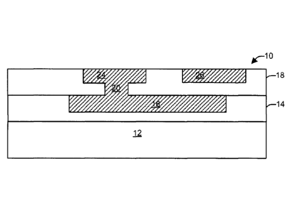
superconducting devices. Therefore, many of the methods used to fabricate
superconducting devices in these laboratories utilize processes or equipment
incapable of rapid, consistent fabrication. Recently there has been a movement
to
mass producing superconducting circuits utilizing similar techniques as those
utilized in
conventional semiconductor processes.
[0005] One well-known semiconductor process is the formation of contacts
and
conductive lines in a multi-level interconnect stack to couple devices to one
another
over different layers of an integrated circuit. One such fabrication process
for formation
1
Date Recue/Date Received 2021-05-18
CA 03060218 2019-10-15
WO 2019/036081 PCMJS2018/033299
of conductive contacts and lines is known as a dual damascene process. Current
dual
damascene processes center around copper (Cu) interconnects for sub 130
nanometer
(nm) integrated circuits (ICs). There is no known current process of filling a
dual
damascene structure with a superconducting metal using semiconductor
deposition
processes.
SUMMARY
[0006] In one example, a method of forming a superconductor interconnect
structure is provided. The method comprises forming a dielectric layer
overlying a
substrate, forming an interconnect opening in the dielectric layer, and moving
the
substrate to a deposition chamber. The method further comprises depositing a
superconducting metal in the interconnect opening, by performing a series of
superconducting deposition and cooling processes to maintain a chamber
temperature
at or below a predetermined temperature until the superconducting metal has a
desired
thickness, to form a superconducting element in the superconductor
interconnect
structure.
[0007] In another example, a method of forming a superconductor dual
damascene structure is provided. The method comprises forming a second
dielectric
layer over a first dielectric layer having a first superconducting element,
etching a
contact opening in the second dielectric layer that extends to and exposes the
first
superconducting element in the first dielectric layer, etching a conductive
line opening in
the second dielectric layer that overlies the contact opening to form a dual
damascene
structure having a dual damascene opening, and moving the dual damascene
structure
to reside on a temperature control chuck in a deposition chamber. The method
further
comprises setting the temperature to the temperature controlled chuck at or
below a
predetermined temperature, and depositing a superconducting metal in the dual
damascene opening while in the deposition chamber to form a dual damascene
structure comprised of a contact and a second conductive line overlying and
coupled to
2
CA 03060218 2019-10-15
WO 2019/036081 PCT/US2018/033299
the contact, such that the contact connects the first conductive line to the
second
conductive line through the second dielectric layer. The depositing the
superconducting
metal comprises performing a series of superconducting deposition and cooling
processes to maintain a chamber temperature at or below the predetermined
temperature until the superconducting metal has a desired thickness.
BRIEF DESCRIPTION OF THE DRAWINGS
[0008] FIG. 1 illustrates a schematic cross-sectional view of a
superconducting
interconnect structure.
[0009] FIG. 2 illustrates a schematic cross-sectional view of an example of
a
superconductor structure in its early stages of fabrication.
[0010] FIG. 3 illustrates a schematic cross-sectional view of a beginning
formation of a first portion of the dual damascene process undergoing an etch
process.
[0011] FIG. 4 illustrates a schematic cross-sectional view of the structure
of
FIG. 3 after the etch process and after the photoresist material layer has
been stripped.
[0012] FIG. 5 illustrates a schematic cross-sectional view of a beginning
formation of a second portion of the dual damascene process undergoing an etch
process.
[0013] FIG. 6 illustrates a schematic cross-sectional view of the structure
of
FIG. 5 after the etch process and after the photoresist material layer has
been stripped.
[0014] FIG. 7 illustrates a schematic cross-sectional view of the structure
of
FIG. 6 undergoing a preclean process.
[0015] FIG. 8 illustrates a cross-sectional view of the deposition chamber
during
the deposition process showing the deposition of niobium ions onto the surface
of the
superconductor structure.
[0016] FIG. 9 illustrates a zoomed in cross-sectional view of the via and
trench
opening, and the deposition process showing the deposition of niobium ions
onto the
surface of the superconductor structure.
3
CA 03060218 2019-10-15
WO 2019/036081 PCT/US2018/033299
[0017] FIG. 10 illustrates a schematic cross-sectional view of the
structure of
FIG. 7 after undergoing deposition of a superconductor liner in the deposition
chamber.
[0018] FIG. 11 illustrates a schematic cross-sectional view of the
structure of
FIG. 10 after a contact material fill to deposit a number of subsequent
intermediate
superconducting material layers in the deposition chamber.
[0019] FIG. 12 illustrates a schematic cross-sectional view of the
structure of
FIG. 11 after a contact material fill to deposit a number of final
intermediate
superconducting material layers in the deposition chamber.
[0020] FIG. 13 illustrates a schematic cross-sectional view of the
structure of
FIG. 12 after undergoing a chemical mechanical polish.
DETAILED DESCRIPTION
[0021] The present disclosure describes a method to fill an interconnect
structure
with a superconducting metal. Vias and trenches of the interconnect structure
are filled
with a deposition process that employs a series of deposition and cool step
sequences
to maintain temperatures at or below 150 C. In one example, the temperatures
are
maintained at or below 90 C. This is achieved by depositing the metal film,
turning off
the deposition power, of for example, a deposition chamber, and allowing the
wafer to
cool before the next deposition cycle occurs. This is repeated until the metal
film is
deposited to the appropriate thickness for forming contacts and/or conductive
lines.
[0022] In one example, a method is provided to fill a dual damascene
structure
with a superconducting metal using a physical vapor deposition (PVD)
deposition
process. It has been demonstrated that a dual damascene dielectric structure
can be
filled successfully with little to no voids by performing the above series of
deposition and
cool step sequences using a PVD chamber.
[0023] In another example, the method utilizes a PVD tool that is capable
of
providing power to a superconducting material slab of about 5 kW (5,000 W) to
about 30kW (30,000W) with AC bias assistance to the wafer in the range from
4
CA 03060218 2019-10-15
WO 2019/036081 PCT/US2018/033299
about 100W to about 500W to sputter a superconducting film in a damascene
structure.
The film properties allow for superconducting properties below 30K within the
damascene structure.
[0024] In yet another example, a superconducting material is sputtered due
to the
ionization of a gas molecule, such as Argon, which collides with a
superconducting
target and knocks off metal atoms from the target surface. The sputtering
process is
controlled by the process variables mentioned above. The process alters the
direction
of sputtered ionized metal atoms toward the substrate by the attraction to the
biased
substrate and having a coil with tunable deposition rate by applying AC power
between
about 0 to about 1500W and DC power between about 0 to about 500W. The tunable
coil impacts the ionization rate of the metal which is then accelerated to the
substrate,
for example, at an angle between 45 -90 , such that the angular distribution
of ionized
metal atoms is controlled by the coil power.
[0025] FIG. 1 illustrates cross-sectional view of a superconductor
interconnect
structure 10. The superconductor interconnect structure 10 includes a first
dielectric
layer 14 overlying a substrate 12, and a second dielectric layer 18 overlying
the first
dielectric layer 14. The substrate 12 can be formed of silicon, glass or other
substrate
material. Both the first and the second dielectric layers 14 and 18 can be
formed of a
low temperature dielectric material that can be employed in low temperatures
(e.g., less
than or equal to 150 degrees Celsius) typically utilized in the formation of
superconducting devices. A first conductive line 16 is embedded in the first
dielectric
layer 14. A first conductive contact 20 extends from the first conductive line
16 at a first
end to a second conductive line 24 in the second dielectric layer 18, and a
second
conductive contact 26 is disposed in the second dielectric layer 18 overlying
a portion of
the first conductive line 16. Each of the contacts and conductive lines are
formed of a
superconducting material, such as niobium. Each of the conductive lines and
conductive contacts are formed with a deposition process that employs a series
of
deposition and cool step sequences to maintain temperatures at or below 150 C
(e.g.,
CA 03060218 2019-10-15
WO 2019/036081 PCT/US2018/033299
at or below 90 C). This is achieved by depositing the metal film, turning off
the power
and allowing the wafer to cool before the next deposition cycle occurs. This
is repeated
until the metal film is deposited to the appropriate thickness.
[0026] Turning now to FIGS. 2-13, fabrication is discussed in connection
with
formation of interconnects in the superconducting device of FIG. 1. It is to
be
appreciated that the present example is discussed with respect to a process
flow that
starts with the formation of either a single or dual damascene layer of
superconducting
metal in an insulating dielectric. The present example will be illustrated
with respect to
a single damascene trench etched into a dielectric thin film to form a bottom
conductive
line followed by a dual damascene process to form top conductive lines.
[0027] FIG. 2 illustrates a cross-sectional view of a superconductor
structure 50
in its early stages of fabrication. The superconductor structure 50 includes a
first
dielectric layer 54, that overlays an underlying substrate 52. The underlying
substrate 52 can be, for example, a silicon or glass wafer that provides
mechanical
support for the first dielectric layer 54 and subsequent overlying layers. A
first
conductive line 56 resides within the first dielectric layer 54 and has a top
surface that is
flush with a top surface of the first dielectric layer 54. The first
conductive line 56 is
formed from a superconductive material and can be formed by a series of
deposition
and cool step sequences to maintain temperatures at or below 150 C until the
metal film
is deposited to the appropriate thickness. In another example, a series of
deposition
and cool step sequences are performed to maintain temperatures at or below 90
C until
the metal film is deposited to the appropriate thickness.
[0028] A second dielectric layer 58 is formed over the first dielectric
layer 54.
Any suitable technique for forming the first and second dielectric layers may
be
employed such as Low Pressure Chemical Vapor Deposition (LPCVD), Plasma
Enhanced Chemical Vapor Deposition (PECVD), High Density Plasma Chemical Vapor
Deposition (HDPCVD), sputtering or spin-on techniques to a thickness suitable
for
providing an interconnect layer.
6
CA 03060218 2019-10-15
WO 2019/036081 PCT/US2018/033299
[0029] FIG. 3 illustrates a beginning formation of a first portion of the
dual
damascene process. As illustrated in FIG. 3, a photoresist material layer 62
has been
applied to cover the structure and patterned and developed to expose via
opening 64 in
the photoresist material layer 62 in accordance with a via pattern. The
photoresist
material layer 62 can have a thickness that varies in correspondence with the
wavelength of radiation used to pattern the photoresist material layer 62. The
photoresist material layer 62 may be formed over the second dielectric layer
58 via spin-
coating or spin casting deposition techniques, selectively irradiated (e.g.,
via deep
ultraviolet (DUV) irradiation) and developed to form the via opening 64.
[0030] FIG. 3 also illustrates performing of an etch 200 (e.g., anisotropic
reactive
ion etching (RIE)) on the second dielectric layer 58 to form extended via
opening 66
(FIG. 4) in the second dielectric layer 58 based on the via pattern in the
photoresist
material layer 62. The etch step 200 can be a dry etch and employ an etchant
which
selectively etches the underlying second dielectric layer 58 at a faster rate
than the
underlying conductive line 56 and the overlying photoresist material layer 62.
For
example, the second dielectric layer 58 may be anisotropically etched with a
plasma
gas(es), herein carbon tetrafloride (CF4) containing fluorine ions, in a
commercially
available etcher, such as a parallel plate RIE apparatus or, alternatively, an
electron
cyclotron resonance (ECR) plasma reactor to replicate the mask pattern on the
photoresist material layer 62 to thereby create the extended via opening 66.
The
photoresist material layer 62 is thereafter stripped (e.g., ashing in an 02
plasma) so as
to result in the structure shown in FIG. 4.
[0031] As represented in FIG. 5, a photoresist material layer 68 is applied
to
cover the structure of FIG. 4, and is then patterned and developed to expose
open
trench regions 70 in the photoresist material layer 68 in accordance with a
trench
pattern. FIG. 5 also illustrates performing of an etch 210 (e.g., anisotropic
reactive ion
etching (RIE)) on the second dielectric layer 58 to form partially extended
openings 72
(FIG. 6) based on the trench pattern in the photoresist material layer 68. The
etch 210
7
CA 03060218 2019-10-15
WO 2019/036081 PCT/US2018/033299
also removes layers of niobium oxide and portions of dielectric oxide formed
during the
various processes and not covered by the photoresist material layer 68. The
photoresist material layer 68 is thereafter stripped so as to result in the
structure shown
in FIG. 6. The extended opening 72 is co-aligned with the via opening 66 to
form a dual
damascene opening.
[0032] During the stripping of the photoresist material layer 68, and the
transfer of
the structure through one or more transfer/buffer chambers, oxides build up on
the
superconducting metal and on the second dielectric layer 58. This results in
the
formation of a metal-oxide 74, such as niobium oxide, on the top surface of
the
conductive line 56 degrading performance. This metal-oxide layer 74 has a
deleterious
effect on the superconducting properties of the first conductive line 56.
Therefore, the
structure is transferred to a preclean chamber to remove oxides from the
superconducting metals prior to depositon. The oxides can be removed by
peforming a
sputter etch. The structure undergoes an etch process 210 to remove the
metal-oxide 74, and portions of dielectric oxide (not shown) formed on the
second
dielectric layer 58.
[0033] As shown in FIG. 8, the structure is moved to a deposition chamber
110.
The deposition chamber 110 is setup with a slab of target material, such as
niobium
(Nb), disposed on a top surface of the chamber 110, and a wafer disposed on a
temperature controlled chuck. To control the wafer temperature, an
electrostatic chuck
(ESC), which uses conductance to transfer heat to and from the wafer
controlled
between about 15 C to about 150 C (e.g., at or below 90 C), provides
repeatable
results and tighter specifications of the film properties. A DC bias (5-30KW)
is applied
to the slab of superconducting material and an AC Bias (100-500W) is applied
to the
wafer on the chuck. An AC/DC coil is located around the periphery of the
substrate and
the coil power (DC power (0-500W) and AC bias power (0-1500W)) changes the
amount of angular ionization which ionizes metal neutrals projected to the
substrate with
an angle between 45 -90 .
8
CA 03060218 2019-10-15
WO 2019/036081 PCT/US2018/033299
[0034] Argon is injected into the chamber, which bombards the slab causing
Nb
ions to be directed to the structure 50, and thus deposition of the Nb into
vias and
trench openings. The RF Coil/DC Coil provides directionality of the Nb ions
based on a
desired angular ionization. FIG. 9 illustrates a zoomed in view of the via and
trench
opening being filled with Nb ions to result in the deposition of a
superconducting Nb
material layer filling the via and trenches and covering the overlying second
dielectric
layer.
[0035] As previously stated, the formation of the superconducting lines and
vias
undergo a series of deposition and cooling steps to not allow overheating of
the
structure 50 above 150 C. This is achieved by depositing the metal film,
turning off the
power and allowing the wafer to cool before the next deposition cycle occurs.
This is
repeated until the metal film is deposited to the appropriate thickness. It
has been
discovered that the various parameters can be altered to promote better
damascene fill
which impacts superconducting properties. These include but are not limited to
DC
power (5-30KW) applied to the target material, bias power (100-500W) applied
to the
wafer, DC power (0-500W) and RF power (0-1500W) to coils to assist in
deposition
directionality, and base vacuum and pressure selection during deposition.
[0036] In the demonstrated process, the initial deposition deposits a metal
such
as Nb as a liner, which is very conformal to the damascene structure as
illustrated in
FIG. 10. The liner is deposited to allow a thin coating (10-25nm) conformal
metal film
that allows successive metal depositions to form preferential grain structure
which
enable the metal film to fill the damascene structure.
[0037] One example for depositing a first layer or liner of superconducting
material is as follows. First, the chuck is set and maintained at a
temperature of
about 75 C to about 100 C (e.g., 90 C). Next, when the wafers enters the
chamber
and is clamped on the ESC chuck an Argon gas is flowed to the backside of the
wafer
through a gas line in the ESC at about 5 to about 6 standard cubic centimeters
(sccm)
to allow for heat transfer through conductance. Heat transfer to or from the
wafer helps
9
CA 03060218 2019-10-15
WO 2019/036081 PCT/US2018/033299
control the temperature of the wafer during processing. The chamber is then
front-filled
with about 5 to about 90 sccm (e.g., 83 sccm) of Argon, the processing gas.
Next, DC
power is applied to the slab of about 500 Watts for about 2 seconds to
initiate the
plasma process. The DC power is increased to about 20,000 Watts, the wafer AC
bias
power is set to about 100 to about 500 watts, while the RF Coil power is
increased to
about 1100 Watts causing the superconducting material to be deposited in the
via and
trench opening for about 20 to 40 seconds. Next a cooling step is performed by
turning
off the DC power, AC bias power, and coil power for about 40 to 200 seconds,
depending on how long it takes for the wafer to cool back down to initial set
temperature.
[0038] A number of subsequent intermediate superconducting material layers
78
are then deposited over the superconducting liner 76 to provide the resultant
structure
shown in FIG. 11. Furthermore, a number of subsequent final superconducting
layers 80 are deposited over the intermediate superconducting material layers
78 to
form the resultant structure of FIG. 12.
[0039] Each time an additional superconducting layer is deposited, the
sequence
is repeated of applying DC power to the slab of about 500 Watts for about 2
seconds to
initiate the plasma process, increasing the DC power to about 20,000 Watts, AC
bias
power to about 100 to about 500 Watts, while the RF Coil power is increased to
about 1100 Watts causing the superconducting material to be deposited in the
via and
trench openings for about 20 to 40 seconds, and repeating a cooling step by
removing
the DC power, AC bias power, and coil power for about 40 to 200 seconds. After
the
final layer is deposited, a final cooling step is performed for about 10 to 60
seconds, and
a pumping process is performed to clear the Argon from the deposition chamber
and
remove the pressure from the chamber which takes about 5 seconds.
[0040] Following deposition of the final layer of the contact material
fill, the
structure is removed from the deposition chamber 110, and is polished via
chemical
mechanical polishing (CMP) down to the surface level of the dielectric layer
58 to form a
CA 03060218 2019-10-15
WO 2019/036081 PCT/US2018/033299
first contact 82, a second conductive line 84, and a third conductive line 86
to provide
the resultant structure of FIG. 13.
[0041] What have been described above are examples of the invention. It is,
of
course, not possible to describe every conceivable combination of components
or
methodologies for purposes of describing the invention, but one of ordinary
skill in the
art will recognize that many further combinations and permutations of the
invention are
possible. Accordingly, the invention is intended to embrace all such
alterations,
modifications, and variations that fall within the scope of this application,
including the
appended claims.
11