Note: Descriptions are shown in the official language in which they were submitted.
CA 03060398 2019-10-18
WO 2018/195148 PCT/US2018/028078
INTERNATIONAL PCT PATENT APPLICATION
APPARATUS AND METHOD OF AGGREGATING AND SUPPLYING ENERGY
Cross Reference to Related Applications
[0001] This is an International Patent Application which claims priority
to U.S. Non-
Provisional Application No. 15/954,993, filed on April 17, 2018, and to U.S.
Provisional
Application No. 62/486,654 filed April 18, 2017, both entitled "METHOD AND
APPARATUS
OF AGGREGATING AND SUPPLYING ENERGY" the entirety of each of which is
incorporated
herein by reference.
Field of the Invention
[0002] The invention relates generally to the field of aggregating,
generating and supplying
electric energy. More specifically, the invention is directed to an apparatus
and method of
aggregating such energy from multiple and diverse generation sources,
regulating and controlling
the generated energy, and optimally supplying the generated energy to a load,
independently, or
supplying the generated energy to a utility grid or supplying the energy
generated to both the load
and the utility grid. The apparatus of the invention is sometime referred to
herein as the "energy
server" or simply the "server".
Background
[0003] In recent years, the adverse effects of climate change and global
warming have led
to an increased interest in renewable energy as a clean and abundant energy
source. A global effort
is underway to transition away from fossil fuel based electrical energy
generation to renewable
generation. However, this transition has significant technical, political and
geopolitical challenges
that need to be overcome.
CA 03060398 2019-10-18
WO 2018/195148 PCT/US2018/028078
[0004] Renewable energy is abundantly available everywhere in the world.
However,
renewable energy is intermittent, non-dispatchable (which means that it cannot
be turned on and
off as required) and depending on geography and the type of renewable energy,
is available for
only limited amounts of time during a day.
[0005] The energy requirements of communities and of the world generally,
however, are
for a continuous supply of stable electricity, 24-hours a day.
[0006] Many existing electricity networks are currently designed to
deliver a continuous
supply of stable electricity, 24-hours a day. However, their design is usually
based on predictable
sources of energy and, dispatchable generation that is available 24-hours a
day.
[0007] Because grid networks are designed for predictable, disptachable
generation that is
available 24-hours a day, it has limitations that include the need for large
sums of capital to grow
the network and long lead times to build infrastructure, the interdependence
of which causes vast
areas of the network to concurrently fail and causes major maintenance and
upkeep requirements.
[0008] Due to these limitations, especially the need for large capital
expenditures required,
there are still about 1.3 billion people in the world who do not have any, or
proper, access to
electricity.
[0009] Therefore, in order to overcome the limitations of the existing
grid infrastructure
and uniqueness of renewable generation, distributed energy solutions have to
be developed that
enable electricity to be generated and consumed in the same location. These
solutions must consist
of renewable generation technologies, such as photovoltaics solar ("PV"),
wind, energy storage
(batteries), and a control system that enables the generation, regulation,
control and delivery of
continuous, stable electricity 24-hours a day.
[0010] The solution to this problem is believed to lie in providing
different generation
sources to be aggregated and the generated energy regulated and controlled.
Then, the aggregated
energy can be supplied to energy storage systems for availability during non-
generation times. The
load will thus be managed.
2
CA 03060398 2019-10-18
WO 2018/195148 PCT/US2018/028078
[0011] Currently, attempts are being made to build such solutions by
combining multiple
sources of renewable energy, including other generating systems such as the
utility grid, various
types of energy storage, into a single system with an AC and/or a DC output.
This typically requires
connecting each individual energy generation source to a central controller,
designing complex
software that monitors the load profile and dispatches energy from the
appropriate source and
managing the multiple communications protocols between the various energy
sources, the
controller and the load. Such integration typically requires complex software
customized for each
deployment. While such deployments are being rolled out, they are inadequate
to meet the needs
of a proper transition from fossil fuels to a renewable based energy network.
Summary of the Invention
[0012] To replace fossil fuels, control electronics must deliver all the
functionality that the
grid network now delivers, as well as delivering stable, continuous and
resilient power. Therefore,
it is important to note that all the features necessary to operate a network
are designed and available
in the sever of the present invention, thus making them work optimally with
each other. By
eliminating multiple hardware systems and software components which are
typically supplied
from different manufacturers, the energy server also eliminates risks of
incompatibility, thus
delivering a more stable and resilient solution than a solution that is
composed of different
products.
[0013] Consistent with the foregoing and in accordance with the invention
as embodied
and broadly described herein, an apparatus and method of aggregating energy
from multiple and
diverse generation sources, regulating and controlling the generated energy,
and optimally
supplying the generated energy to a load, independently, or supplying the
energy generated to the
utility grid or supplying the energy generated to both the load and the
utility grid is described in
suitable detail to enable one of ordinary skill in the art to make and use the
invention.
[0014] Specifically, the invention is directed to an apparatus and a
method for aggregating
and supplying energy. The apparatus includes a plurality of power modules for
inverting a first
type of electrical power (such as DC power), which is supplied to said power
modules from
multiple disparate sources of power, to a second type of electrical power
(such as AC power) at an
output of each of the power modules for storage for future use, or for driving
an electrical load or
3
CA 03060398 2019-10-18
WO 2018/195148 PCT/US2018/028078
for transmitting to a central or regional grid. A first busbar (such as a DC
busbar) is connected
with the multiple disparate sources of power and is also connected with the
plurality of power
modules for providing the first type of electrical power thereto. A second
busbar (such as an AC
busbar) is connected with an output of each of the plurality of power modules
for receiving said
second type of electrical power from said power modules and for making said
second type of
electrical power available for use at a destination. A power microcontroller
is carried by and
incorporated within each of said power modules, and each power microcontroller
is configured for
controlling power inversion operations of said power modules. The discharge
microcontroller is
further configured for generating controlled pulses of charge and discharge
for increasing storage
capacity of the at least one energy storage device. A control module is
connected with said plurality
of power modules, and an interface may be connected with the control module
for effecting
communication with external devices. At least one energy storage device
external to the server
can be in communication with the plurality of power modules for receiving
electrical energy from
their output. The at least one energy storage device can also have a plurality
of cells for receiving
and storing energy output from the power modules. A charging module and a
discharge
microcontroller supported by the charging module is configured by an algorithm
based pulse width
modulator ("PWM") for continually monitoring the at least one energy storage
device. The power
microcontrollers are configured for generating, from said plurality of power
modules,
controlled pulses of charge and discharge for increasing storage capacity of
the energy storage
device. A control microcontroller is carried by and incorporated within the
control module and is
connected with the at least one energy storage device, the control
microcontroller is configured for
determining and monitoring voltage levels within the at least one energy
storage device and for
rebalancing voltage within said at least one energy storage device. Sensor
devices are positioned
in contact with said at least one energy storage device continually sensing
voltage levels within
the at least one energy storage device, said sensors being in communication
with the control
microcontroller for supplying sensed data thereto. A communication and
automation module
("CAM") is supported by the control module and in communication with the
control
microcontroller. The CAM has a programmable dry output for monitoring and
interfacing with the
control microcontroller and responding to events within the server that are
monitored and detected
by sensors.
4
CA 03060398 2019-10-18
WO 2018/195148 PCT/US2018/028078
[0015] The method of the invention includes receiving a first type of
electrical power (such
as DC power) from multiple disparate sources through a first busbar (such as a
DC busbar),
directing said first type of electrical power to a plurality of power modules
for inverting said first
type of electrical power to a second type of electrical power (such as AC
power) at an output of
said power modules, delivering said second type of electrical power from said
power modules to
a second busbar (such as an AC busbar) connected with the plurality of power
modules,
and making the second type of electrical power from said power modules
available to a location
for use, such as an electric load, a storage device, or a national or regional
grid system, or an energy
storage device. The method also includes controlling various operations of the
power
modules through a power microcontroller incorporated within each of said power
modules, said
power microcontroller configured for effecting said control, and controlling
and operating said
power modules through a control module connected with the power modules. The
control module
has a control microcontroller carried by and within said control module.
Generating controlled
pulses of charge and discharge is performed from said power module thereby
increasing storage
capacity of said energy storage device. The method further includes sensing
voltage levels
within the energy storage device and supplying sensed voltage levels to the
control microcontroller
which is configured for rebalancing voltage within said energy storage device,
and monitoring said
sensed voltage levels by said control microcontroller, as well as detecting
lagging or leading power
factor based on sensed data and for charging capacitance or inductance as
required to correct said
lead or lag, the control microcontroller is connected with said energy storage
device and configured
for said monitoring. And the method includes monitoring and responding to
events within the
server that are monitored by sensors through a communication and automation
module
("CAM") supported by said control module and in communication with said
control
microcontroller.
[0016] Other features, embodiments and aspects of the inventions are
further described
herein below.
Brief Description of the Drawings
[0017] The features and advantages of the present invention will be more
fully disclosed
in, or rendered obvious by the following detailed description of the preferred
embodiments, which
CA 03060398 2019-10-18
WO 2018/195148 PCT/US2018/028078
are to be considered together with the accompanying drawings wherein like
numbers refer to like
parts and further wherein:
[0018] Fig. 1 is a front elevation view of a chassis supporting elements
and modules of the
invention;
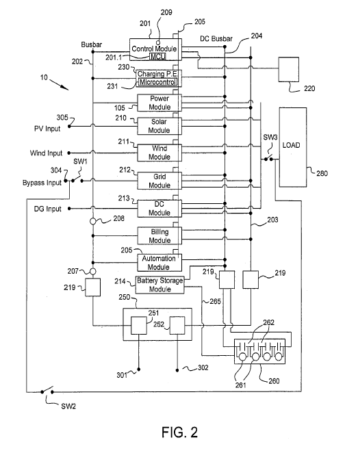
[0019] Fig. 2 is a schematic diagram illustrating the overall system
architecture embodying
the principals of the invention;
[0020] Fig. 3 is a partial schematic diagram showing one aspect of the
system of Fig. 2;
[0021] Figs. 4(a) and 4(b) are schematic illustrations of voltage
conversion transformers
incorporated in the invention when using a system with medium or high voltage
lines;
[0022] Fig. 5 illustrates a communication and automation module (the
"CAM"), as a
universal converter for communicating with a control module of the invention;
[0023] Fig. 6 is a circuit diagram of a static switching circuit used in
the present invention;
[0024] Fig. 7 is a circuit diagram illustrating an AC to DC rectifier
used in the present
invention;
[0025] Fig. 8 is a schematic diagram of the inverter (power) module used
in the present
invention for connecting the AC input busbar, the AC output busbar, the DC
busbar and the
communication busbar of the chassis shown in Fig. 1;
[0026] Fig. 9 is a schematic illustration of the arrangement and
connections for the power
module of the present invention;
[0027] Fig. 10 is a flow diagram illustrating the startup sequence when
the inverter module
shown in Fig. 8 is plugged into the chassis illustrated in Fig. 1;
[0028] Fig. 11 is a circuit diagram of the inverter module illustrated in
Fig. 8; and
[0029] Fig 12 is a circuit diagram illustrating the elements for
effecting correction of
lagging or leading power factor.
6
CA 03060398 2019-10-18
WO 2018/195148 PCT/US2018/028078
Description of Embodiments of the Invention
[0030] The following disclosure includes embodiments, or examples, for
implementing
different features of the invention. Specific examples of components and
arrangements are
described below to simplify the present disclosure. These are, of course,
merely examples and are
not intended to be limiting. Terms concerning electrical coupling and the
like, such as "coupled,"
"connected" and "interconnected," refer to a relationship wherein structures
communicate with
one another either directly or indirectly through intervening structures
unless expressly described
otherwise. For the sake of simplicity, all connections and communication links
between and
among referenced devices, structures and elements, which are discussed and
described herein, may
not actually be shown or illustrated in the accompanying drawings, or they may
not be shown
because such connections or links are not amenable to being shown in the
drawings.
However, those skilled in the art will understand and appreciate the existence
of such connections
and links from the descriptions herein and from the context in which they are
described. In
addition, the present disclosure may repeat reference numerals and/or letters
in the various
examples. This repetition is for the purpose of simplicity and clarity and
does not in itself dictate
a relationship between the various embodiments and/or configurations
discussed.
[0031] The description below together with the annexed drawings,
illustrate and describe
an illustrative example of the energy server 10 of the present invention for
aggregating, managing,
converting, inverting and controlling energy from different types of inputs
and storage media. The
server is completely flexible and scalable due to its modular design and
incorporates unique
features described below.
[0032] Referring first to Fig. 1, a chassis 100 serves as the
infrastructure platform for the
energy server 10 of the invention and includes a casing (or "rack") 101 with
slots 102 for receiving
and supporting various modules and elements of the invention. In one
embodiment of the
invention, which is exemplary, the following system modules are supported in
the slots of the rack
101: a monitor module 103; charger module 104; and power modules 105 (multiple
power modules
105 may be provided). Surge protective devices 106 and 107 may also be
provided in the power
lines to each of the modules for protection. Input, output and bypass circuit
breakers 108, 109 and
110 respectively may also be provided in the input, output and bypass lines
(as discussed below)
7
CA 03060398 2019-10-18
WO 2018/195148 PCT/US2018/028078
for further system protection. The power modules 105 (sometime referred to
herein also as the
"inverter modules" or "inverter") have a sine wave curve that is configured to
operate at a very
high resolution of 1024 bits per quarter cycle as opposed to existing
inverters that operate at 16
bits per quarter cycle. This high speed switching of field-effect transistor
("FET") devices is
achieved through the use of wide bandgap gallium nitride devices (also known
as GaN FET) and
configuring the microcontroller in the power module to enable the use of GaN
devices to generate
a sine wave with very high resolution of 1024 bits per quarter cycle.
[0033] Silicon (Si) technology has displaced almost all prior low power
thermionic and
electromechanical devices, but fundamental material limitations have stalled
its use in higher
power applications. GaN devices are now available for high power applications.
Advantages of
GaN devices include: reduced heat sink requirements; 80% reduction in system
volume and
weight; lower voltage drop for unipolar devices; increased output power;
improved transient
characteristics and switching speed; reduced electrical noise from smaller
system packages; and
reduced electrical noise due to virtually zero recovery charge.
[0034] The power module handles very high torque loads of up to 1000%
generated by
reactive loads as opposed to current inverters which handle a maximum of 250%.
High torque
loads generated by all reactive loads are handled by combining the properties
of the high resolution
sine wave (as described above) and operating at high input DC voltages (384VDC
¨ 1200VDC).
The power module DC to AC efficiency is extremely high, over 96% for reactive
loads and over
99% for resistive loads. Such high efficiencies are achieved by combining the
high speed / low
loss switching (as above) and high operating DC voltage (384VDC ¨ 1200VDC).
[0035] The power module 105, functions primarily as an inverter of DC
power to AC
power. Fig. 9 schematically illustrates the arrangement and connections of the
power module 105.
Accordingly, the power module 105 includes a microcontroller unit ("MCU") 903,
which is
configured for controlling the operations of the power module. Input operating
voltage is supplied
to the MCU 903 through a voltage and inspection element 902, which is supplied
with operating
voltage from a 3 phase main electricity input 901. Input 901 also feeds
voltage to a rectifier switch
904 which supplies rectified voltage to a harmonic filter 905. The harmonic
filter 905 is configured
for limiting voltage fluctuations and improving the operations of the power
module. Such filters
8
CA 03060398 2019-10-18
WO 2018/195148 PCT/US2018/028078
are commercially known and available. Filter 905 then feeds a 6 or 12 pulse
rectifier 906 for
rectifying the voltage signal. MCU 903 is configured to control the operation
of the rectifier via
rectifier spring circuit 907. The rectified voltage signal is then fed from
the rectifier 906 to both a
bus filter 908 for feeding into the MCU 903, and to a DC bus filter 910 which
supplies power both
to batteries 260, which are external to the server, and to off grid inverter
911, which is connected
to the load directly. Power from the DC bus filter 910 also supplies power to
a battery voltage and
circuit controlling bus protection unit 912. The battery voltage and circuit
controlling bus
protection unit 912 then feeds back to the MCU 903, which in turn operates a
charging voltage
circuit controlling protection 913 and an input voltage default phase
rectifier 914. Batteries 260
can be a variety of types, including for example multi-cell chemical
batteries.
[0036] During normal operation, AC power from a grid network is supplied
at the AC input
901 and goes through rectifier switch 904, filter 905, rectifier 906, then
busbar 910, to inverter 911
and to a load 280, or to external battery 260. During this time, PV energy
controlled by internal
MPPT, supplies power to charge the battery 260. When the grid is not
available, such as due to an
outage on the grid, the system seamlessly shifts the supply to battery and PV
from an external PV
panel which produces energy from sunlight 920 through a solar controller then
to the load 280 to
power the load, or the system seamlessly shifts the supply to the battery 260
and then to the load,
therefore ensuring continuous power supply. During daylight hours, with
sufficient PV input and
with grid power available, power will be provided from the solar panels and
will be adjusted by
the solar controller into the maximum power supply condition to supply the
load, while grid input
is on standby, and to concurrently charge the battery 260 with any excess
power.
[0037] During night time hours, also with grid power available, power
will be supplied
from the external battery 260 (which has been charged from PV solar panels
during the daylight
hours), which discharges to a pre-set value (with a reserve for emergency
use). If the battery 260
is fully discharged before the PV panels start producing the next day, the
system will switch
automatically to the grid, supplying power to the load until PV input starts
again. On cloudy / rainy
days, with insufficient sunshine to charge the battery, but with grid power
available, power will
first be supplied by the PV solar panels and any excess will concurrently
charge the battery 260.
When the PV power is no longer available, the battery will supply power to the
load 280 until it is
discharged to a pre-set value (keeping a reserve for emergency use),
subsequent to which the
9
CA 03060398 2019-10-18
WO 2018/195148 PCT/US2018/028078
system will switch automatically to the grid to supply power to the load. At
night, with the grid
not available, battery power will be used.
[0038] During periods of maintenance, power from the grid can be supplied
through a by-
pass switch to power the load 208.
[0039] Although not readily visible in Fig. 1, but as seen in Fig. 2, the
chassis 100 also
includes AC input busbar 202, AC output busbar 203, DC busbar 204 and
communication busbar
205, as well as a control module 201 which, are supported by the casing (rack)
101. The control
module 201 includes a communication and automation module (CAM) 205, which may
be
mounted as a separate element in the rack 101, as further described herein
below. As noted above,
the various functional modules, in practice, are inserted in the slots 102 for
support in the chassis
100, connected to the busbars via safety screws (not shown), and are
controlled and operated by
the control module 201.
[0040] Control module 201 communicates with an interface 220 (such as a
graphical user
interface), for effecting communication with external devices or systems
having different
protocols. The interface 220 employs well known industry standards for
communication protocols
in machine communications, such as USB, RS232, RS485, and dry contact.
[0041] Each busbar is connected to either an input or an output through
thermal circuit
breakers 108, 109 and 110. Current, voltage and temperature sensors 207, 208
and 209,
respectively are connected on these busbars to provide data to the control
module 201. Other
devices (not shown) such as cooling fans and air-conditioners, as is typical,
may also be installed
in the chassis 100 for cooling purposes, depending on the type and size of the
energy server.
[0042] One or more power modules 105 (which may include a solar power
module 210, a
wind power module 211, a grid power module 212, and a diesel generator ("DG")
power module
213) are also supported in the chassis 100 carried by casing 101. The power
modules operate (as
illustrated and described in connection with Fig. 9) to invert input voltage
and then make that
supply power available to at least one external battery (such as battery 260)
and to the load 280.
Load 280 can be any type of AC load, reactive or resistive, and is driven from
all the disparate
input (AC/DC) energy sources. In addition to standard maximum power point
tracking ("MPPT")
function, the solar and wind modules increase the storage capacity of standard
Lead Acid / AGM
CA 03060398 2019-10-18
WO 2018/195148 PCT/US2018/028078
/ Gel / LiFePo4 batteries by 40% and enable operation of a super-capacitor,
lead acid or lithium
ion battery at 100% depth-of-discharge without affecting cycle life. (Current
solar charge
controllers and wind charge controllers do not have such functionality). The
microcontroller
carried by each of the solar or wind power modules is configured by an
algorithm to drive a set of
controlled pulsating bursts of charge and discharge in short durations. This
activity, which is
monitored and controlled by the microcontroller within the solar or wind
module, results in
increasing the ionic density of the electrolyte inside the chemical battery
(but only for lead acid,
AGM and gel batteries), hence increasing its storage capacity. An additional
benefit of increasing
storage capacity is the ability to safely operate the battery at depth-of-
discharge of 100% without
effecting cycle life.
[0043] Although, for convenience, only a single battery 260 is
illustrated in Fig. 2, it should
be readily understood that when referring to "battery 260" or to "a battery"
or "the battery" herein,
it is intended to include multiple batteries ganged together, or an array of
batteries that are
connected in series and parallel to the server 10. Such batteries may also
have multiple cells 262.
Individual batteries in the connected array can develop an imbalanced charging
state due to
manufacturing tolerances which can result in the imbalanced batteries becoming
damaged over
time. In order to protect the batteries from damage, the server continually
monitors the condition
of each individual cell in the array through cell sensors 261 and balances
each cell by drawing
charge from cells in an overcharged state and supplying the charge to cells in
an undercharged
state. Sensors 261 monitor voltage, temperature and internal resistance of
every cell and convey
that data to a microcontroller within battery storage module 214 via R5484
communication line
265 for thus controlling the balancing of the cells.
[0044] Each battery 260 is controlled by discharge microcontroller 231,
supported by
charging module 230, and configured by an algorithm based pulse width
modulator ("PWM") that
continually monitors cell voltage and compares it with the other cells in the
battery. When an
imbalance of overcharge is detected, the discharge controller draws the charge
from the
overcharged cell and supplies this to an auxiliary battery cell connected to
the controller from
where it is supplied back to the cell with the lowest charge. In this way
active battery balancing is
achieved.
11
CA 03060398 2019-10-18
WO 2018/195148 PCT/US2018/028078
[0045] The AC input busbar 202 (for various configurations or
embodiments, such as: 3
phase 440V 50Hz ; 3 phase 220V 60Hz ; 1 phase 220V 50Hz ; or 1 phase 110V
60Hz) is mounted
in the chassis 100 through 1500V AC isolators 219 and is connected to the
various modules and
other system elements through the micro-switch connectors 113 in the module
slots (see Fig 1).
The AC input busbar 202 is thus isolated and the various modules are hot
swappable (as used
herein, the expression "hot swappable" is intended to mean that a module can
be removed or
installed without operationally shutting down the chassis or system). The AC
input busbar 202 is
capable of handling an input of 2x its rated capacity (in kW) as a constant
load and 10x its rated
capacity (in kW) as an instantaneous load for 2s. Such busbars are well known
in the art and are
commercially available to consumers in the electrical and electronic arts.
[0046] The various disparate inputs of power (whether solar, wind,
turbine, diesel
generator, grid, geothermal, battery, or any other AC or DC source) connected
to the server 10 can
be blended in a pre-determined percentage and delivered with regulated power
quality output. All
such input energy sources (i.e. AC, DC, battery), as well as the server's
internal capacitor storage,
are regulated on a common DC busbar 204 which is the primary source that
drives the inverters.
In case of transfer of one energy source to the other, as signaled by a
central control microcontroller
(the "control microcontroller") 201.1 carried by the control module, the
battery and/or capacitor
storage provide interim energy to the DC busbar until the transfer between
sources is completed.
As a result, the inverter stays fully energized during the transition and
therefore, switching between
sources is seamless and virtually instantaneous.
[0047] Control microcontroller 201.1 of the control module 201 is in
communication with
the power modules' output connections and thus with the load 208. A control
logic of the control
microcontroller 201.1 detects lagging or leading power factor on the circuit
load and is configured
to effect power factor correction. With reference to Fig. 12, the control
microcontroller 201.1,
symbolically illustrated in Fig. 12 by the terminal notation 201.1, is also
configured so that it then
charges an embedded single large capacitor C-1 or inductor L-1 in the server,
with exactly the
capacitance or inductance required to correct the lag / lead. The capacitor C-
1 or inductor L-1 then
supplies the exact capacitance or inductance to correct the lag or lead. The
value of the capacitance
or inductance is controlled by the switching of IGBT-1 and IGBT-2 as
determined and
implemented by control microcontroller 201.1
12
CA 03060398 2019-10-18
WO 2018/195148 PCT/US2018/028078
[0048] A control logic of the control microcontroller 201.1 continually
detects and
analyses resonated harmonics frequencies being generated by reactive loads. It
then calculates the
R, L, C (resistor, inductor, capacitor) values and applies these values on a
circuit (such circuit
being formed by the closed current path created through load at the output
terminals) to filter out
the unwanted frequencies.
[0049] Not shown in Figs. 1 or 2, but as illustrated in Fig. 3, a thermal
circuit breaker 340,
of appropriate rating, is positioned in between the AC input 301 and the AC
input busbar 202, for
input overload safety. Similarly, circuit breakers 341, 342, 343, 344 and 345
are positioned
between the AC output 302 and AC output busbar 203, the battery input 303 and
battery/storage
module 214 (which can also be supported in chassis 100), bypass input 304 and
bypass/power
module 215, PV input 305 and solar module 210 and solar input 306 and wind
module 211,
respectively. Voltage and hall effect current sensors are also installed on
the busbar to monitor for
the current and voltage by the control module 201.
[0050] The AC output busbar 203 (3 phase 440V 50Hz / 3 phase 220V 60Hz /
1 phase
220V 50Hz / 1 phase 110V 60Hz) is mounted in the chassis 100 through 1500V AC
isolators 219
and is connected to the various modules and other system elements through the
connectors such
as 113 in the module slots 102. The AC output busbar 203 is isolated and the
modules are hot
swappable. The AC output busbar 203 is capable of handling an output of 2x its
rated capacity (in
kW) as a constant load and 10x rated capacity (in kW) as an instantaneous load
for 2s. Thermal
circuit breaker 341 shown in Fig. 3, of appropriate rating is positioned in
between the AC output
302 and the AC output busbar 203 for output overload safety. Voltage, hall
effect current and other
sensors (such as sensors 207, 208 and 209, see Fig. 1) are also installed on
the busbar to monitor
for current and voltage by the control module.
[0051] The DC busbar 204 is also mounted in the chassis 100 through 1500V
DC isolators
219 and is connected to the various modules and other system elements or
devices through the
connectors, such as 113, in the module slots 102. DC busbar 204 is isolated
and the modules are
hot swappable. The DC busbar 204 is capable of handling 2x its rated DC
capacity (in kW) as a
constant load and 10x its rated DC capacity (in kW) as an instantaneous load
for 2s. The Voltage
13
CA 03060398 2019-10-18
WO 2018/195148 PCT/US2018/028078
hall effect current and other sensors (such as sensors 207, 208 and 209, see
Fig. 1) are positioned
on the busbar to monitor for the current and voltage by the Control Module.
[00521 A 4 wire duplex communication busbar 205 is connected to a
connector 113 in
every module slot 102 of the chassis 100 and is the channel for communication
between the various
modules.
[0053] The following are the input and output connectors installed in the
chassis module
100: AC input 301; AC output 302; battery input 303; storage input (DC);
bypass input (AC) 304;
PV input (DC) 305; wind input (DC/AC) in the wind module; and generator input
(AC) (the bypass
input is also used as generator input).
[0054] All inputs and outputs are installed through circuit breakers 340-
345 for overload
protection, as illustrated in Fig. 3.
[0055] Each of the slots in the rack 101 of the chassis 100 for receiving
and supporting the
various system modules and other system elements carries micro-switch
connector 113. This
micro-switch 113 is depressed when a specified safety screw in the inserted
module is tightened.
Once the micro-switch 113 is depressed, an electric signal is transmitted to
the control module 201
and provides data about the inserted module thereby allowing the control
module to initiate the
initialization process of the inserted module, synchronizing it with the
operating modules in the
system. Inserting modules into the slots, and removing them from the slots, is
a seamless operation
that can be performed while the energy server is in operation, providing
continual operability, and
therefore prevents power disruption.
[0056] A voltage conversion chassis module 250 contains voltage
conversion transformers
251 and 252 at the input and output, respectively of the chassis 250 so that
the input and output
operating voltages can be converted according to the requirements. This is
used when using the
chassis module 250 with medium or high voltage lines. Once connected, the
input and output
voltages of the chassis module 250 can be converted to medium or high
voltages. Figs. 4(a) and
4(b), schematically illustrate voltage conversion transformers 251 and 252 for
converting input
and output voltages, respectively. In the example illustrated in Fig. 4(a) a
primary input voltage
of 11KV is stepped down to a secondary voltage of 400V by the input voltage
conversion
14
CA 03060398 2019-10-18
WO 2018/195148 PCT/US2018/028078
transformer 251. In the example shown in Fig. 4(b), a primary output voltage
of 400V is stepped
up to a secondary voltage of 11KV by the output voltage conversion transformer
252. In an
embodiment of the invention, the voltage conversion transformers are an
integral part of the server,
so no external or separate chassis, such as chassis 250 would be required.
[0057] The communication and automation module (the "CAM") 205,
schematically
illustrated in Fig. 5, is a universal protocol converter embedded with serial
ports 501 (RS232), 502
(RS485/RS422) and 503 (TCP/IP Ethernet port). The CAM communicates with the
control module
201 through a 64-bit parallel port 504 and then converts this communication to
different protocols.
The CAM 205 supports MODBUS, MODBUS over TCP/IP, MODBUS over RS485, CANBUS,
PROFIBUS and S BUS.
[0058] The CAM also has an 8-port dry contact output 505 that is user
programmable.
Each port is programmable to respond to a specific event determined by various
sensors throughout
the server, such as low battery alarm, system overload, battery disconnect,
inverter shutdown,
static bypass, grid failure, module failure etc. or to respond to any event in
the system.
[0059] The CAM 205 also incorporates a programmable automation feature to
communicate with external devices that may be connected to the System. This
automation feature
of the CAM 205 communicates with the control module 201 also on the same 64-
bit port 505.
[0060] While the CAM 205 has a separate slot in the chassis 100, it
operates as an integral
part of the control module 201 and if unplugged will cause a shut down of the
control module 201,
hence shutting down the server system.
[0061] The grid/charging module 230 operates to: (i) convert AC into DC
voltage; (ii)
charging battery 260 using a bi-directional DC to DC converter; and (iii) for
static switching
between bypass and inverter in case of inverter failure and inverter restart.
[0062] When the grid/charging module 230 is plugged into its slot in the
chassis 100, it
operates to connect the busbars through a special hot swappable connecter.
[0063] The grid/charging module 230 incorporates a microcontroller 231,
which is
configured in order to perform the following:
CA 03060398 2019-10-18
WO 2018/195148 PCT/US2018/028078
(i) detect if input DC voltage is present on the DC busbar;
(ii) detect that the safety screw is in place;
(iii) confirm if the input DC voltage is within the correct range;
(iv) confirm if the input AC voltage is within the correct range;
(v) check if a handshake signal is present on the communication busbar 205;
(vi) connect with the control module 201 through the communication busbar 205;
(vii) receive its module number assignment from the control module 201; and
(viii) communicate with the control module to receive instructions on usage of
grid input
which is either:
a. to switch grid input statically at the output and shut down the inverter
(static
switching mode); or
b. to switch on the AC to DC rectifier, then convert the grid input to DC and
merge
this DC power with the DC busbar 204. The DC power is merged in accordance
with a policy programmed by a user and communicated to the grid / charging
module 230 by the control module 201 (AC to DC rectification mode); or
c. to switch on the AC to DC rectifier in current limiting mode, then convert
the
grid input to DC and merge this DC power with the DC busbar to supply the
inverter (AC to DC rectification and current limiting mode).
[0064] Once the grid/charging module 230 is started in any of the above
modes, it
continuously communicates with the control module 201 to receive operating
instructions about
current limiting value or changing the mode. The operation of each mode is
described below
[0065] The static switching mode is accomplished, as shown in Fig. 6,
through the static
switch 600 which incorporates combination switching of bi-directional silicon
controlled rectifier
("SCR") in forward and reverse connection, which are also connected to the PWM
microcontroller
231. There are 2 SCR pairs operating in single-pole double-through mode
(common 601 connected
to the load, NC 602 (normally closed contact) connected to the inverter, NO
603 (normally open
contact) connected to the bypass terminal). Once the PWM microcontroller
receives the
instructions from the control module, it switches from NC to NO mode. The
switching time from
NC to NO mode is completed in 5ms. This bypass switch arrangement is used to
connect an
emergency power source to the load 280 in case of inverter failure or any
other failure of energy
16
CA 03060398 2019-10-18
WO 2018/195148 PCT/US2018/028078
source which may result in zero power at the output. The static bypass
switches the load 280 to a
pre-defined energy source statically by the user. Switching time is 4ms with
Phase Locked Loop
("PLL") synchronization. This is achieved using semi-conductor static devices
(SCR ¨ Silicon
Controlled Rectifier). No electromechanical relay is used. The manual bypass
is an
electromechanical switch connected on the terminal post of the server which is
manually operated
by the user. This manual bypass can be used for maintenance. Once the manual
bypass is engaged
the power is bypassed from the terminal posts and maintenance can be done
anywhere inside the
system. In case of an overload or short circuit on the output load the
Server's auto bypass function
automatically bypasses the load to the grid through the static bypass switch.
In case the grid is not
available or overload / short circuit is greater than 200% of the sever
capacity, the internal safeties
shutdown the server. This functionality is achieved through the control module
microcontroller
201.1 monitoring the output current / load ¨ this detects the overload or
short circuit and signals
the static bypass switch to transfer the load from the inverter directly to
the grid and in case of no
grid availability or overload greater than 200%, to shut down the server.
[0066] The switching response time is 5ms i.e. the time counted from the
occurrence of
failure until the restoration of backup power. In case of an overload or short
circuit on the output
load 280 the auto bypass function automatically bypasses the load to the grid
through the static
bypass switch 600. In case the grid is not available or overload / short
circuit is greater than 200%
of the sever capacity, the internal safeties (described herein) shutdown the
server. This
functionality is achieved through the microcontroller 201.1 monitoring the
output current / load ¨
this detects the overload or short circuit and signals the static bypass
switch 600 to transfer the
load from the inverter directly to the grid and in case of no grid
availability or overload greater
than 200%, to shut down the server.
[0067] The AC to DC rectifier mode, illustrated in Fig. 7, consists of a
PWM mode
switching power supply with a bridge mode rectifier and an inductor -
capacitor circuit ("L-C
circuit") filter which is connected to an insulated gate bipolar transistor
(IGBT-7) shown in Fig. 7
that is controlled by a PWM microcontroller 701 configured to control the IGBT-
7. The IGBT-7
switches the DC power of a power inductor and transfers the discharge power
from the inductor
to the DC busbar 204 after filtering it through a short key rectifier and an
output capacitor. This
entire process is regulated by the PWM microcontroller 701 with feedback from
the voltage and
17
CA 03060398 2019-10-18
WO 2018/195148 PCT/US2018/028078
current sensors at the DC output. The L-C circuit can act as an electrical
resonator, an electrical
analogue of a tuning fork, storing energy oscillating at the circuit's
resonant frequency. The IGBT
is a three-terminal power semiconductor device primarily used as an electronic
switch which, as it
was developed, came to combine high efficiency and fast switching.
[0068] In AC to DC rectification and current limiting mode, the process
of rectification is
monitored by a control logic in the microcontroller 231 in the charging module
230 and the current
is limited based on optimizing the load and battery state-of-charge ("SOC").
The control logic
continually checks the load and battery SOC and limits the current so that the
load operates safely
and the battery is not overcharged.
[0069] The rectification process starts and continues after the PWM
microcontroller 231
(which runs the pulse width modulation function) receives information from the
control
microcontroller 201.1 of control module 201 regarding the AC input voltage and
whether or not
that the AC input voltage is within the correct range (which is to be
programmed by the user). In
case the AC input voltage falls outside the set range, the control
microcontroller 201.1 shuts down
the process. When the AC input voltage returns to the set range, the control
microcontroller 201.1
restarts the process.
[0070] The rated power of each module is 20kW or 50kW or 100kW. In an
overload event,
the PWM microcontroller 201.1 shuts down the process immediately. The PWM
microcontroller
201.1 analyzes the load situation after 60s-120s (time is programmed by the
user). If the overload
persists it remains shutdown unless reset manually.
[0071] The power module 105 (or, as noted above "inverter module"), shown
in Fig. 8, is
a hot swappable module and includes connections with the following busbars: AC
input busbar
202; AC output busbar 203; DC busbar 204; and communication busbar 205. A
circuit diagram of
the inverter module is illustrated in Fig. 11. The power module also has a
communication port 81
for contact with the communication busbar 205, an output port 82 for providing
output power to
the AC output busbar 203 a DC input port for contact with the DC busbar 204,
an AC input port
84 for contact with the AC input busbar 202, a bypass input port 85 for
contact with bypass input
304 and a configuration port 86.
18
CA 03060398 2019-10-18
WO 2018/195148 PCT/US2018/028078
[0072] The inverter module 201 operates to invert DC input from the DC
input busbar into
AC output on a pre-defined frequency (50Hz or 60Hz) and output voltage (90V or
110V or
220V/240V per phase). The inverter module 201 then synchronizes the AC output
at the AC output
busbar of the chassis 100.
[0073] When the first inverter (power) module is plugged into its slot in
the chassis 100, it
connects to the various busbars through special hot swappable connecters. The
startup sequence
process is shown in Fig. 10.
[0074] MCU 903 of the inverter (power) module 201 is configured so that
when the first
inverter module is plugged into the chassis 100 at step 1001, the MCU 903
within of the inverter
module performs the following further steps. Step 1002 detects if input DC
voltage is present on
the DC busbar. If yes, it then detects at 1003 if the safety screw is in
place. If not, the step is
repeated. If yes, MCU 903 then confirms at step 1004 if the input DC voltage
is within the correct
range. Then, it checks at 1005 if the handshake signal is present on the
communication busbar 205.
Next, at 1006, it connects with the control module 201 through the
communication busbar 205 and
receives its module number assignment from the control module 201.
[0075] After the first inverter module ("Module 1") has received its
module number
assignment, then Module 1 waits at 1007 for a phase-locked loop ("PLL") signal
from the control
module 201 to indicate that the phase is related to the phase of the input
signal. When it receives
the PLL signal from the control module at 1008, then MCU 903 starts this
inverter module at step
1009, and at 1010 enables initiation for safety checks programmed into MCU 903
for a DC
overvoltage, a DC under voltage, an AC overvoltage, an AC under voltage, and
an AC
synchronization failure.
[0076] For module 2...n, its respective MCU then: detects at 1011
synchronization (zero
crossing) detect on AC busbar; receives at 1012 the PLL signal from the
control module 201, then
starts at 1013 this inverter module; and at 1014 enables safety algorithms
for: DC overvoltage; DC
under voltage; AC overvoltage; AC under voltage; and AC synchronization
failure.
[0077] An off-grid inverter 911 is connected to the load directly.
Therefore, all the
attributes of the load 280 have to be directly handled by the inverter. This
problem becomes tedious
19
CA 03060398 2019-10-18
WO 2018/195148 PCT/US2018/028078
when the load is reactive. The only way the inverter can handle these problems
is with a high-
resolution sine wave. It has been established that the minimum resolution that
can effectively
handle the problems of the load is 1024 bits per quarter cycle.
[0078] To achieve this resolution a Digital Signal Processer ("DSP")
microcontroller 903
is configured for every quadrant of the sine wave cycle. This signal is then
fed to a power drive
containing Gallium Nitride power transistors which are connected in bridge
mode that are
switching between positive and negative DC lines at a frequency of 205kHz PWM
duty cycle.
This results in the output of a high-resolution sine wave (1024 bits per
quarter cycle). The DC
input is as follows:
= 20kW rated module: 300VDC ¨ 420VDC with optimal voltage being 384VDC.
= 50kW rated module: 500VDC - 725VDC with optimal voltage being 600VDC
= 100kW rated module: 1000VDC ¨ 1450VDC with optimal voltage being 1200VDC
[0079] Because the sine wave generated is high-resolution, it enables the
handling of high
torque loads for short durations because it does not get distorted with
instantaneous currents
generated by the load. The schematic of the Inverter Module is shown in Fig. 9
below.
[0080] Overvoltage and under voltage protection is provided by the
control module
microcontroller being configured to continually monitor the voltage of the DC
input. If the DC
input voltage exceeds the maximum or minimum present limit, the control module
microcontroller
shuts down the inverter (power) module in order to protect it. In case the
electronic shutdown
doesn't work, a fast blow safety fuse and a circuit breaker (not shown, well
known in the art) do
their job.
[0081] Overload protection is also provided by the control module
microcontroller by it
being configured to continually monitor the output load from the sensors on
the output lines. The
configured protection allows the following overload condition:
Maximum of 1000% for 2s
Decreasing to 200% over the next 8s
CA 03060398 2019-10-18
WO 2018/195148 PCT/US2018/028078
[0082] If the overload condition continues beyond this profile, the
control module
microcontroller instantly shuts down the inverter (power) module to protect
it.
[0083] However, if the overload remains within 200%, the configuration of
the
microcontroller allows operation for another 30 minutes with an alarm. During
these 30 minutes,
the control module microcontroller 201.1 monitors the condition of the battery
storage by
communicating with the control module. If the control module microcontroller
senses that the
battery storage is unable to support the overload, even if it is within the 30-
minute duration, the
control module microcontroller shuts down the inverter module.
[0084] When the module is inserted into the Chassis, and if this isn't
the first module, the
control microcontroller checks the voltage of AC output busbar before
switching on and
synchronizing the Inverter. If the voltage is not within the set limits, the
Inverter is not switched
on, nor synchronized and an alarm is raised. This condition is also
communicated to the Control
Module.
[0085] As the inverter module is synchronizing with the AC output busbar,
it constantly
monitors through the current sensors the positive and negative current
situation. In case a negative
energy is detected dumping into the inverter that is flowing in reverse
direction meaning synch
failure. In this situation the control microcontroller communicates with the
control module to get
the appropriate PLL synch signal within lms. If this is not rectified the
control module
microcontroller shuts down the inverter module to protect it.
[0086] In order to protect all inputs and outputs, a fast blow fuse is
connected on all inputs
and outputs of the inverter module. In case of failure of the electronic
shutdown safeties described
above, the fast blow input and output fuses protect the module.
[0087] As described, three different microcontrollers simultaneously
control all the
components and functions of the server through a common communication bus. In
case one
microcontroller hangs due to any reason, the watchdog seamlessly transfers the
control to the
redundant microcontroller within the same machine cycle so there is no loss of
instruction and the
control remains uninterrupted. The third microcontroller always remains as a
backup and maintains
the storage of different settings and sensors data.
21
CA 03060398 2019-10-18
WO 2018/195148 PCT/US2018/028078
[0088] While the invention has been illustrated and described in
connection with currently
preferred embodiments shown and described in detail, it is not intended to be
limited to the details
shown since various modifications and structural changes may be made without
departing in any
way from the spirit of the present invention. The embodiments were chosen and
described in order
to best explain the principles of the invention and practical application to
thereby enable a person
skilled in the art to best utilize the invention and various embodiments with
various modifications
as are suited to the particular use contemplated
22