Note: Descriptions are shown in the official language in which they were submitted.
PHOTOVOLTAIC DEVICES WITH DEPLETED
HETEROJUNCTIONS AND SHELL-PASSIVATED
NANOPARTICLES
This is a divisional application stemming from CA 2,795,719, filed March 25,
2011.
BACKGROUND OF THE INVENTION
1. Field of the Invention
10001] This invention resides in the fields of photovoltaic cells and quantum
dots.
2. Description of the Prior Art
100021 Solar cells that generate electricity through the photovoltaic effect
require a combination
of low cost and high efficiency in order for such cells to offer a practical
alternative to traditional
means of power generation. One way in which the cost of manufacturing a
photovoltaic cell can be
lowered is by the use of solution processing to form the layer of light-
harvesting material that is part
of the cell. The efficiency of thc cell, however, depends on the cell
materials, including the light-
harvesting material. The optimal light-harvesting material is one that
achieves a high short-circuit
current density Jõ by maximizing the absorption of the sun's rays in both the
visible and infrared
spectra, and that one extracts a high level of work, in the form of a high
open-circuit voltage V, and
a high fill factor FF, from each absorbed photon. For an input solar intensity
Psolar (typically 100
mW cm-2), the power conversion efficiency ri is defined as
[0004] It has been reported by Sargent, E., in "Infrared photovoltaics made by
solution
processing," Nat. Photonics 3, 325-331 (2009), and Hillhouse H.S., et al., in
"Solar cells
Voc.1 scFF
=
solar
[0004] It has been reported by Sargent, E., in "Infrared photovoltaics made by
solution
processing," Nat. Photonics 3, 325-331(2009), and Hillhouse H.S., et al., in
"Solar cells
from colloidal nanocrystals: Fundamentals, materials, devices, and economics"
Curr. Opin. Colloid
Interface Sci. 14, 245-259 (2009), that the use of colloidal quantum dots as
the light-harvesting
material provides photovoltaic cells with high power conversion efficiencies.
Colloidal quantum
dot photovoltaics offer both the ability to form the light-harvesting layer by
solution processing and
the ability to tune the bandgap over a wide range, benefits that are available
in both single-junction
and multijunction cells. The ability to tune the bandgap also enables the use
of inexpensive,
abundant ultralow-bandgap semiconductors that are otherwise unsuitable for
photovoltaic energy
1
CA 2795719 2017-08-21
CA 3061443 2019-11-13
conversion. By combining lead chalcogenide quantum dots and Schottky
junctions, photovoltaic
cells with efficiencies of 3.4% have been achieved, as reported by Ma, W., et
al., "Photovoltaic
devices employing ternary PbSõSel,Nanocrystals," Nano Lett. 9, 1699-1703
(2009), and others.
Significant progress has also been achieved by sensitizing nanoporous TiO2
electrodes with a thin
layer of colloidal quantum dots, with power conversion efficiencies of 3.2%.
See for example Fan,
S., et al., "Highly efficient CdSe quantum-dot-sensitized TiO2 photoclectrodes
for solar cell
applications," Electrochem. Commun. 11, 1337-1330 (2009).
100031 Both colloidal quantum dots and Schottky devices pose certain
limitations photovoltaic
efficiencies, however. In Schottky devices, both the V, and the FF values have
fallen well below
their potential, and in cells sensitized by colloidal quantum dots, the ./.õ
values are generally lower
despite the increases in Vo, and FF.
SUMMARY OF THE INVENTION
100041 It has now been discovered that the limitations of colloidal quantum
dot photo voltaics as
noted above can be significantly reduced or overcome by the pairing of a layer
of light-harvesting
nanoparticles with a layer of an electron-accepting material such that the
junction between these
layers is substantially depleted of both free electrons and free holes on at
least one side of the
junction when the device is not illuminated. An effective means of achieving
this depletion is by
selecting materials for these two layers that are of different bandgap
magnitudes. Such a junction is
thus a heterojunction by virtue of the two different materials on either side
of the junction, and in
particular a depleted heterojunction by virtue the low level or absence of
both free electrons and
free holes in the vicinity of the junction. The depletion arises from charge
transfer from the
electron-accepting contact to the to the nanoparticles. In certain embodiments
of the invention, the
nanoparticles are quantum dots, include p-type colloidal quantum dots, and the
electron-accepting
layer is, or includes, a metal oxide. The depletion is at least partly
attributable to a relatively low
charge density in the electron-accepting layer, as compared to that of the
metal contact of a
Schottky junction, which has a very high free electron density.
100051 Particular embodiments of photovoltaic devices within the scope of this
invention offer
further advantages over photovoltaic devices of the prior art. For example,
the use of a metal oxide
as the electron-accepting layer allows the device to be configured with the
electron-accepting layer
as the front surface of the device or as the layer that the solar rays first
penetrate upon entering the
two semiconductor layers that form the photovoltaic junction. The electrons
liberated by the rays
2
CA 2795719 2017-08-21
CA 3061443 2019-11-13
are thus less susceptible to recombination with the holes since the electrons
in these embodiments
have a shorter distance to travel before reaching their destination electrode.
Also, in embodiments
in which the junction is that between a metal oxide and quantum dots, the
junction is better defined
and easier to passivate, and thus less susceptible to defects, than a metal-
semiconductor Schottky
junction. This avoids the occurrence of Fermi-level pinning at the interface.
Still further, these
embodiments present less of a barrier to hole injection than a Schottky device
by introducing a large
discontinuity in the valence band and by minimizing the electron density at
the interface.
[0006] It has further been discovered that the performance of nanocrystals in
photovoltaic devices
and in optoelectronic devices in general, and particularly nanocrystals with
surface anions, is
enhanced by depositing cations over the nanocrystals to form a first or inner
shell and deposing
anions over the first shell to form a second or outer shell. The inner and
outer shells together
passivate surface defects on the nanocrystal which tend to disrupt the quantum
confinement of the
nanocrystal. Passivation is known to be achievable by the placement of short
organic ligands such
as ethanedithiol, butylamine, or mercaptopropionic acid on the nanocrystal
surface. The use of
cation and anion shells in place of these ligands offers the advantages that
the cation shells bind to
the anions on the nanocrystal surface rather than to the cations, as organic
ligands tend to do, and
the ionic bonds are stable upon exposure to air and light, and particularly
moisture, oxygen, and
heat. Further advantages of these cation and anion shells are that by avoiding
the need for organic
ligands, these shells allow the nanocrystals to reside very close to each
other in the light-absorbing
film and thereby promote electron wave function overlap and carrier mobility,
valuable features that
are typically impeded by organic ligands.
BRIEF DESCRIPTION OF THE FIGURES
[0007] FIG. 1 is a plot of current density vs. voltage for examples of
depleted heterojunction
photovoltaic cells within the scope of the present invention.
[0008] FIG. 2 is a plot of current vs. voltage for examples of depleted
heterojunction photovoltaic
cells within the scope of the present invention.
[0009] FIG. 3 is a plot of external quantum efficiency vs. wavelength for
examples of depleted
heterojunction photovoltaic cells within the scope of the present invention.
[0010] FIG. 4 is a plot of device capacitance vs. bias voltage and device
resistance vs. bias voltage
for examples of depleted heterojunction photovoltaic cells within the scope of
the present invention.
3
CA 2795719 2017-08-21
CA 3061443 2019-11-13
[0011] FIG. 5 shows absorption spectra of examples of depleted heterojunction
photovoltaic cells
with dual-shell-passivated quantum dots within the scope of the present
invention.
[0012] FIG. 6 is a plot of carrier lifetime vs. light intensity for examples
of depleted
hetcrojunction photovoltaic cells with dual-shell-passivated quantum dots
within the scope of the
present invention.
[0013] FIG. 7 is a plot of current density vs. voltage for examples of
depleted hetcrojunction
photovoltaic cells with dual-shell-passivated quantum dots within the scope of
the present
invention.
DETAILED DESCRIPTION OF ILLUSTRATIVE EMBODIMENTS
OF THE INVENTION
[0014] The term "substantially depleted" as used herein to characterize the
region(s) adjacent to a
heterojunction dcnotcs that the charge density in the region(s) is orders of
magnitude less than that
of the metal side of a Schottky junction. In certain heterojunction regions of
the invention, the
charge density is three or more orders of magnitude less than the charge
density of conducting
metals, and in many of these, the charge density is four or more, five or
morc, or six or more orders
of magnitude less. Particularly effective results can be achieved when the
depleted charge density
is on the n-type electron accepting layer side of the junction. In many
embodiments of the
invention, a range of charge density in the depleted region is about 1 x 10¹²
cm-1 to about 1 x 10¹⁸
cm-1, or alternatively about 1 x 1014 cm-1 to about 1 x 1017 cm-1, or as a
further alternative about 1 x
1015 cm-1 to about 1 x 1016 cm-1.
[0015] To achieve a depleted heterojunction by use of materials of different
bandgap magnitudes
on the two sides of the junction, effective results in many cases can be
achieved with a bandgap
difference (i.e., the difference between the bandgap magnitude on one side of
the junction and the
bandgap magnitude on the other side of the junction) of at least about 1.5eV,
or within the range of
from about 1.5eV to about 5eV, or even more effectively within the range of
from about 2eV to
about 5eV. With an n-type electron-accepting layer on one side of the junction
and p-type light-
absorbing nanoparticles on the other, the bandgap of greater magnitude will
reside in the n-type
electron-accepting layer.
[0016] Quantum dots are particularly useful as the nanoparticles, and
colloidal quantum dots, i.e.,
quantum dots manufactured by colloid chemistry, are notable examples. Of
these, metal
4
CA 2795719 2017-08-21
CA 3061443 2019-11-13
=
chalcogenide quantum dots are well known in the art, and lead chalcogenide,
and particularly lead
sulfide, quantum dots are of particular interest. Quantum dots are known to
absorb light at
wavelengths related to the diameters of individual quantum dots, and this
property can be used in
the present invention to select or optimize the light-absorbing
characteristics of the quantum dots.
In many cases, quantum dots with a number-average diameter within the range of
about 2nm to
about 15nm can be used effectively, while those with a number-average diameter
within the range
of about 3nm to about 10nm are often the most appropriate, and among these the
range of about
3nm to about 6nm are often even more useful.
[0017] The n-type electron-accepting layer can vary widely in composition,
provided that the
combination of n-type electron-accepting layer and light-absorbing
nanoparticles when placed in
contact form the depleted heterojunction described above. Metal oxides are
examples of materials
that can serve effectively as the n-type electron-accepting layer, and a
particularly useful example of
a metal oxide is titanium dioxide.
[0018] In those aspects of the invention that relate to nanoparticles with
inner passivating shells of
cations and outer passivating shells of anions, the core of such a
nanoparticle is generally a quantum
dot having exposed anions at its surface. As noted above, the quantum dot core
is in many cases a
metal chalcogenide colloidal quantum dot, most often a metal sulfide colloidal
quantum dot. A
noted example is lead sulfide, and lead sulfide quantum dots are often lead
rich, with a surface
composed primarily of exposed Pb2+ ions but also containing exposed S2" ions.
The cations of the
inner shell bind to, and thereby passivate, the 82- ions at the core surface,
while the anions in the
outer shell bind to, and thereby passivate, the cations of the inner shell.
Examples of cations that
can be used for the first shell are Cd2+, Pb2+, Zn2+, and Sn2+. Among these,
Cd2+ is particularly
convenient and effective. Examples of anions effective for use as the second
shell are halogen ions
and the thiocyanate ion. Of these, halogen ions, and particularly bromine ion,
are optimal or
particularly convenient in certain cases. These dual-shelled nanoparticles are
useful as the light-
absorbing nanoparticles of the depleted heteroj unctions described above, but
are also useful in
optoelectronic devices in general, i.e., any devices in which the particles
serve to absorb light
energy and convert the absorbed energy to an electric current.
[0019] In further aspects, therefore, the present invention resides in the
formation of passivated p-
type semiconductor nanoparticics without using organic ligands as passivating
agents. This is
achieved by treating p-type semiconductor quantum dots that have surface
anions with a solution of
CA 2'795719 2017-08-21
CA 3061443 2019-11-13
a cation-containing reagent that passivates the surface anions, and then
treating the resulting cation-
treated quantum dot core with a solution of a reagent that contains anions
that passivate the cations.
Noting the example of Cd2+ as a cation useful for the passivation of the
quantum dot core, an
example of a Cd2+-containing reagent is cadmium(II) chloride-
tetradecylphosphonic acid-
oleylamine. Examples of anion-containing reagents are quaternary ammonium
halides and
thiocyanatcs, and specific examples are cetyltrimethylammonium bromide,
hexatrimethylammonium chloride, tetrabutylammonium iodide, and
tetrbutylammonium
thiocyanate.
[0020] Photovoltaic devices utilizing one or more of the features described
above will typically
contain at least two electrodes, one electrically connected to each of the two
semiconductor layers
of the heterojunction. In a heterojunction between a n-type metal oxide layer
and a layer of p-type
metal chalcogenide colloidal quantum dots, for example, a first electrode will
be in direct electrical
contact with the n-type metal oxide layer and a second electrode will be in
contact with the colloidal
quantum dot layer. The first electrode in many cases is a light-transmitting
electrode, and examples
are aluminum oxide, zinc oxide, indium tin oxide (ITO), and fluorine-doped tin
oxide (FTO). The
second electrode in many cases is either nickel, lithium fluoride, platinum,
palladium, silver, gold,
or copper, or alloys of two or more of these metals, such as alloys of silver,
gold, and copper. One
example of a combination of electrode materials is fluorine-doped tin oxide as
the first electrode
and gold as the second electrode.
EXAMPLE 1
[0021] This example illustrates the preparation of depleted heterojunction
photovoltaic cells
within the scope of the present invention, each formed by depositing a layer
of PbS colloidal
quantum dots (approximately 1017 cm-3 n-type doping) of varying diameters --
3.7mn (bandgap
1.3eV), 4.3nm (bandgap 1.1eV), and 5.5nm (bandgap 0.9eV) --over transparent
TiO2 electrodes.
[0022] The TiO2 electrodes were prepared on Sn02:F (FTO)-coated glass
substrates (Pilkington
TEC 15, Hartford Glass, Inc., Hartford City, Indiana, USA) with a TiO2 paste
(DSL-90T, Dyesol
Ltd., Queanbeyan, NSW, Australia) as follows. The FTO substrates were first
rinsed with toluene,
then sonicatcd for twenty minutes in a mixture of Triton in de-ionized water
(1-3% by volume).
Separately, a TiO2 paste was prepared by combining one part by weight TiO2
nanoparticles with
three parts by weight terpineol. The paste was then spin cast at 1500rpm for
ninety seconds on the
TiC14-treated FTO substrates. One edge of each substrate was then wiped free
of the paste with a
6
CA 2795719 2017-08-21
CA 3061443 2019-11-13
swab soaked in isopropyl alcohol to expose a section of claim FTO for
electrical contacting. This
was immediately followed by sintering for one hour on a hotplate at 400 C. The
substrates were
then placed in a bath of 60mM TiC14 in de-ionized water, and baked in the bath
at 70 C for thirty
minutes. They were then rinsed with de-ionized water, dried with nitrogen, and
placed in a 520 C
tube furnace for one hour, then cooled to room temperature. The sample was
then allowed to cool,
and the TiC14 treatment was repeated, followed by a final heating to 520 C.
The substrates were
then placed in individual substrate holders and stored in air for up to one
week prior to further
processing.
100231 PbS colloidal quantum dots were prepared as follows.
Bis(trimethylsilyl)sulphide (TMS,
synthesis grade) (0.18g, lmol) was added to 1-octadecene (10mL), which had
been dried and
degassed by heating to 80 C under vacuum for 24 hours. A mixture of oleic acid
(1.34g, 4.8mmol),
Pb0 (0.45g, 2.0mmol), and 1-octadecene (14.2g, 56.2mm01) was heated to 95 C
under vacuum for
sixteen hours, then placed under Ar. The flask temperature was increased to
120 C and the
TMS/octadecene mixture was injected, causing the temperature to drop to about
95 C, and the flask
was allowed to cool to 36 C. The nanocrystals were precipitated with 50mL of
distilled acetone
and centrifuged under ambient conditions. The supernatant was then discarded,
and the precipitate
was redispersed in toluene, precipitated again with 20mL of acetone,
centrifuged for five minutes,
dried, and again dispersed in toluene (about 200mg m1:1). The nanocrystals
were then placed in a
N2-filled glove box, where they were precipitated twice with methane and then
finally redispersed at
25 or 50mg mL-1 in octane.
[0024] The resulting oleate-capped PbS quantum dots were deposited on the TiO2
by multilayer
spin-coating of the TiO2 surface with 25 or 50 mg/mL solutions of the quantum
dots in octane under
ambient conditions. Each layer was deposited at 2500 rpm, then treated briefly
with 10% 3-
mercaptopropionic acid in methanol to displace the oleate ligand and thereby
render the quantum
dots insoluble, then rinsed with methanol and octane. Fifteen deposition
cycles using the 25mg/mL
dispersion produced thermally stable layers 22nm in thickness on the TiO2
substrate, and eight
deposition cycles using the 50mg/mL dispersion also produced thermally stable
layers of the same
thickness. Each layered medium was then transferred to a glove box with N2
atmosphere and left
overnight. A gold contact was then deposited on the quantum dot layer by DC
sputtering with
5mTorr Ar pressure at a power density of 1 W cm-2 through a shadow mask to
thicknesses of
150nm to 200nm. Spatially-resolved X-ray elemental analyses and transmission
electron
7
CA 2795719 2017-08-21
CA 3061443 2019-11-13
microscopy were performed on a thin section sample prepared by focused-ion-
beam milling, and
revealed very little interpenetration of the quantum dot and TiO2 layers.
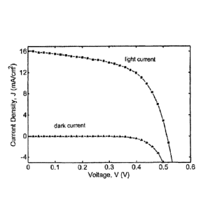
100251 FIG. 1 is a plot of the photovoltaic response of a depleted
heterojunction solar cell as
prepared above, expressed as current density in mA cm-2 vs. voltage, with the
lower curve
representing the dark current and the upper curve representing the illuminated
current of a cell
fabricated with 1.3eV-bandgap quantum dots (3.7nm). The data was measured
using a Keithley
2400 source-meter under ambient conditions. The solar spectrum at AM1.5 was
simulated to within
class A specifications with a Xe lamp and filters with the intensity adjusted
to 100mW cm-2. The
source intensity was measured with a Melles-Griot broadband power meter
(responsive from 300nrn
to 2000nm), through a circular 0.049cm2 aperture at the position of the sample
and confirmed with a
calibrated solar cell. The accuracy of the power measurement was estimated to
be 7%. For the
five devices having 1.3eV-bandgap quantum dots, the average value of Vo, was
0.53 0.02V, the
average value of Jõ was 15.4 1.4mA cm-2, and the average value of FF was 57
4%. The
average AM1.5 power conversion efficiency I/ was thus 4.9 0.3%. For the
highest-performing
device, Vo, was 0.52V, 4, was 16.4mA em-2, and FF was 58%, yielding n of 5.1%.
[0026] FIG. 2 is a plot of the photovoltaic response of a depleted
heterojunction solar cell as
prepared above, expressed as current in rnA vs. voltage, with the lower curve
representing cells
fabricated with 0.9eV-bandgap (5.5nm) quantum dots, the middle curve
representing the cells
fabricated with 1.1eV-bandgap (4.3nm) quantum dots, and the upper curve
representing the cells
fabricated with 1.3eV-bandgap (3.7nm) quantum dots. This figure shows that the
largest quantum
dots had the smallest driving force for electron transfer in TiO2, and yet
devices with these 0.9eV
bandgaps still showed a short-circuit current density 4, above 10mA/cm2 and an
open-circuit
voltage V , of 0.38V. This indicates that minimal band offset is required for
efficient electron
transfer from the PbS colloidal quantum dots into the TiO2 electrode. This is
in contrast to organic
photovoltaics, which have a large band offset between the electron donor and
acceptor, the large
band offset imposing a substantial penalty on efficiency.
[0027] FIG. 3 is a plot of external quantum efficiency (EQE) vs. wavelength
and of absorption vs.
wavelength, with the lower curve representing the EQE for the best-performing
1.3eV-bandgap
quantum dot device and the upper curve representing the spectral absorption of
the same device.
The EQE is the ratio of extracted electrons to incident photons and the curve
is also known as the
incident photon conversion efficiency spectrum. The EQE was obtained by
passing the output of a
8
CA 2795719 2017-08-21
CA 3061443 2019-11-13
400W Xe lamp through a monochromator and using appropriate order-sorting
filters. The
collimated output of the monochromator was measured through a 1.5nm aperture
with a calibrated
Newport 818-UV power meter. The measurement bandwidth was about 40nm and the
intensity
varied with the spectrum of the Xe lamp. The average intensity was 0.3mW cm-2.
The current-
voltage response was measured with Keithley 2400 source-meters. The plot shows
that at short
wavelengths, the EQE reached values above 60%, while at longer wavelengths the
EQE had a peak
of 24%.
[0028] FIG. 4 is a plot of device capacitance vs. bias voltage and of device
resistance vs. bias
voltage. The capacitance arises from the depletion layer due to charge
transfer from TiO2 to the
PbS colloidal quantum dot layer. Capacitance-voltage measurements were
performed directly on
the photovoltaic devices using an Agilent 4284A LCR meter. Absorption
spectroscopy was
performed on a Cary 500 UV-vis-1R Scan photospectrometer. The impedance was
acquired at
2kHz with a signal amplitude of 10mV, and is represented in FIG. 4 in terms of
equivalent parallel
resistance Rp and capacitance Cp for a device with a contact area of 0.03cm3.
The plot shows that
the capacitance, and its associated depletion layer distributed between the
two semiconductors,
persist up to a bias of 0.6V, close to the observed open-circuit voltage
value. This is a direct
indication of the presence of a built-in field that efficiently drives the
separation of photogenerated
carriers.
EXAMPLE 2
[0029] This example illustrates the preparation and use of nanoparticles
containing a quantum dot
core, an inner shell of cations and an outer shell of anions, within the scope
of the present invention.
[0030] Colloidal quantum dots capped with oleic acid ligands were synthesized
and stripped of
their oleate ligands, in the manner described in Example 1. These quantum dots
were prepared with
an excess of Pb during synthesis, resulting in a lead-rich bulk composition
but with sulfur atoms on
their surfaces, either from nonpolar {100} and {11 0} or polar {111} facets in
their crystal structure.
To form the inner shell of Cd cations over these PbS cores, the nanoparticles
were treated with a
solution of CdC12-tetradecylphosphonic acid-oleylamine (CdC12-TDPA-OLA). This
treatment
resulted in a slight redshift (between 6 and 24nm) of the excitonic
absorption, suggesting growth of
a partial monolayer of highly cation-rich material on the surface, an
interpretation reinforced by the
approximately 30nm blueshift observed when a control treatment involving TDPA-
OLA only (no
CdC12) was implemented. Elemental analysis and X-ray photoelectron microscopy
both indicated
9
CA 2795719 2017-08-21
CA 3061443 2019-11-13
0.3% atomic ratio of cadmium to other elements present in powders of the
resultant samples. X-ray
diffraction indicated that no purely Cd-based phase (such as CdS) was present.
[003111 An outer shell of bromine ions was then applied by the use of a
solution of
cetyltrimethylammonium bromide in methanol. The cetyltrimethylammonium cations
combined
= with any remaining oleates on the particles to form salts that were then
removed with a final
methanol rinse. The cetyltrimethylammonium bromide treatment and methanol
rinse were
conducted in air at room temperature (23 C), including the absence of
hydrazine. The absence of
any appreciable amounts of organics at the outer surfaces of the treated
particles was confirmed by
FTIR spectra showing a complete absence of C-H vibrations at 2922cm-1 and
2852cm-1. The
presence of a significant amount of bromide in the outer applied film was
confirmed by X-ray
photoelectron spectroscopy (XPS) and energy-dispersive X-ray spectroscopy
(EDX), and simple
calculation indicated an approximate 1:1 ratio of bromide ions to surface
cations. Elemental
analysis confirmed that the 0.3% of Cd cations present following the initial
CdC12-TDPA-OLA
were still present after application of the bromide shell.
100321 Photovoltaic devices utilizing these dual-shell-passivated quantum dots
were fabricated in
the same manner as described in Example 1 above. A scanning electron
micrograph showed that
the quantum dot layer was approximately 300nm in thickness and was free of the
voids and cracks
that often occur in films made from layer-by-layer deposition. Absorption
spectra of the devices
were obtained in a double pass by including reflection from the Au top
contact. The spectra of
devices made using 9, 11, and 13 quantum dot layers are shown in FIG. 5, which
also includes
corresponding spectra from the bare FTO/TiO2 substrate. The absorption peak at
950nm is the
excitonic peak of the PbS quantum dots. This indicates that quantum
confinement of the core
quantum dots was preserved in the shelled form. A reduction in interparticle
distance is suggested
by the red-shift (--100meV) of the excitonic peak in the final film as
compared to the excitonic peak
of dots in solution. Upon exposure to 100 mW/cm2 solar illumination, the
device showed an open
circuit voltage (V0) of 0.45V, a short-circuit current density (./..õ) of
21.8mA/cm2, and a fill factor
(FF) of 59%, yielding a power conversion efficiency n of 5.76%. Integration of
the net absorption
of the quantum dot film over the AM1.5G spectrum indicates that a film having
100% quantum
efficiency would have achieved a circuit current density (Jõ) of 24.4mA/cm2.
Comparing this with
the measured circuit current density (J) of 21.8mA/cm2 indicates that the
internal quantum
efficiency (IQE) averaged across the entire broadband absorbing region of 400-
1150nm exceeds
90%, indicating minimal recombination loss and efficient carrier extraction.
CA 2795719 2017-08-21
CA 3061443 2019-11-13
[0033] The doping density and carrier lifetime of the dual-shell-passivated
quantum dot films
were determined by capacitance-voltage (C-V) and Võ decay analyses,
respectively. The C-V
analysis showed that doping was a full order of magnitude lower than in the
lowest-doped organic
ligand PbS and PbSe quantum dot films, and the carrier lifetime T, which is
shown in FIG. 6, was
approximately twice as long as that of a control device made using a bidentate
organic ligand (3-
mercaptopropionic acid, also shown in FIG. 6), reaching a remarkably long
lifetime of over 40 sec
even under full solar 100 mW/cm2 illumination.
[0034] The dual-shell-passivated quantum dots also demonstrated an improved
resistance to
oxidation. FIG. 7 is a plot of current density vs. voltage, comparing a layer
of dual-shell-passivated
quantum dots in accordance with the invention with quantum dots bearing 3-
mercaptopropionic
acid ligands, each shown both fresh (immediately after fabrication) and after
ten days of storage
under ambient conditions on a laboratory bench. The dual-shell-passivated
quantum dots showed
no significant change in performance over the ten-day period, while the
organic ligand-capped
quantum dots underwent a complete loss of efficiency over the same period.
[0035] To demonstrate the effectiveness of inner shells of anions other than
bromide ions, devices
were made containing dual-shell-passivated quantum dots with a variety of
anions, and
measurements of the photovoltaic performance characteristics were made. The
anion-bearing
reagents were hexatrimethylammonium chloride (HTAC), cetyltrimethylammonium
bromide
(CTAB), tetrabutylammonium iodide (TBAI), and tetrabutylammonium thiocyanate
(TBAT). The
parameters measured were ./s, in mA/cm2, Võ in V, FF in %, ii in %, shunt
resistance Rh and series
resistance Rõ and rectification (the current between forward bias +1V and
reverse bias -1V), and are
listed in the following Table.
Reagent I,igand 14, Võ FF Rch /34 Rectification
HTAC ci 17.1 0.43 55% 4.08% 3388 1112 10391
CTAB Br" 21.8 0.35 59% 5.76% 3351 60 2920
TBAI r 20.2 0.43 43% 3,76% 3195 148 4916
TBAT SCN" 13.9 0.43 30% 1.72% 1924 847 4232
[0036] In the claims appended hereto, the term "a" or "an" is intended to mean
"one or more."
The term "comprise" and variations thereof such as "comprises" and
"comprising," when preceding
11
CA 2795719 2017-08-21
CA 3061443 2019-11-13
the recitation of a step or an element, are intended to mean that the addition
of further steps or
elements is optional and not excluded. Any discrepancy between any reference
material cited
herein or any prior art in general and an explicit teaching of this
specification is intended to be
resolved in favor of thc teaching in this specification. This includes any
discrepancy between an
art-understood definition of a word or phrase and a definition explicitly
provided in this
specification of the same word or phrase.
12
CA 2795719 2017-08-21
CA 3061443 2019-11-13