Note: Descriptions are shown in the official language in which they were submitted.
CA 03064203 2019-11-19
WO 2019/013840 PCT/US2018/017054
CLOCK FREQUENCY CONTROL SYSTEM
BACKGROUND
[0001] Many systems, for example, radar and radio systems, use an internal
clock
signal for proper operation and synchronization. In these systems, the
internal clock
signal is generated by a clock signal source, for example, a temperature
compensated
crystal oscillator (TCXO) or a voltage controlled crystal oscillator (VCXO).
[0002] The clock signal generated by the clock signal source, however,
drifts over
time and the frequency changes value. If the amount of frequency drift is too
much, the
system may not operate properly. In many instances, the frequency of the clock
signal
source can only be adjusted when the whole system is taken off line for
maintenance.
[0003] What is needed is an approach to controlling a clock signal source
operating
in a system.
SUMMARY
[0004] According to one aspect of the disclosure, a method of operating a
clock
signal source comprises (a) providing a control signal to the clock signal
source; (b)
detecting an output signal from the clock signal source; (c) measuring a value
of a
frequency of the output signal; and (d) comparing the measured frequency value
to an
operating range of frequency values initially bounded by a lower end of an
initial lower
value and an upper end of an initial upper value. If the measured frequency
value is
outside the operating range, then: (d)(1) determining if the frequency of the
output
signal should or should not be changed; and (d)(2) if it is determined that
the frequency
of the output signal should be changed, then modifying the control signal by a
first
predetermined value if the measured frequency is below the operating range or
by a
second predetermined value if the measured frequency is above the operating
range.
The modified control signal is then provided to the clock signal source; and
repeated.
[0005] In another aspect, an apparatus comprises a clock signal source
configured
to provide an output signal; and a first circuit, coupled to the clock signal
source,
configured to: provide a control signal to the clock signal source; measure a
frequency
- 1 -
CA 03064203 2019-11-19
WO 2019/013840 PCT/US2018/017054
value of the output signal; compare the measured frequency value to an
operating
range of frequency values initially bounded by a lower end of an initial lower
value and
an upper end of an initial upper value, and if the measured frequency value is
outside
the operating range, then generate an interrupt signal indicating that the
measured
frequency is too slow or too fast. A processing unit is coupled to the first
circuit and is
configured to, upon receipt of the interrupt signal from the first circuit:
determine if the
frequency of the output signal should or should not be changed; and if it is
determined
that the frequency of the output signal should be changed, then instruct the
first circuit
to modify the control signal by a first predetermined value if the measured
frequency is
too slow or by a second predetermined value if the measured frequency is too
fast.
[0006] In another aspect of the present disclosure, a method of maintaining
a clock
signal source at a first predetermined frequency includes: (a) providing a
control signal
to the clock signal source; (b) detecting an output signal from the clock
signal source;
(c) measuring a value of a frequency of the output signal; and (d) comparing
the
measured frequency value to an operating range of frequency values, the
operating
range initially bounded by a lower end of a first lower value and an upper end
of a first
upper value. If the measured frequency value is less than the first lower
value or greater
than the first upper value, then determining if the operation of the clock
signal source
should or should not be modified to change the frequency of the output signal.
If it is
determined that the operation of the clock signal source should be modified,
then
modifying the control signal by a first predetermined value if the measured
frequency is
less than the first lower value or by a second predetermined value if the
measured
frequency is greater than the first upper value; and providing the modified
control signal
to the clock signal source.
BRIEF DESCRIPTION OF THE DRAWINGS
[0007] Various aspects of the disclosure are discussed below with reference
to the
accompanying Figures. It will be appreciated that for simplicity and clarity
of illustration,
elements shown in the drawings have not necessarily been drawn accurately or
to
scale. For example, the dimensions of some of the elements may be exaggerated
relative to other elements for clarity or several physical components may be
included in
-2-
CA 03064203 2019-11-19
WO 2019/013840 PCT/US2018/017054
one functional block or element. Further, where considered appropriate,
reference
numerals may be repeated among the drawings to indicate corresponding or
analogous
elements. For purposes of clarity, not every component may be labeled in every
drawing. The Figures are provided for the purposes of illustration and
explanation and
are not intended as a definition of the limits of the disclosure. In the
Figures:
[0008] Figure 1 is a block diagram of a system in accordance with an aspect
of the
present disclosure;
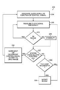
[009] Figure 2 is a flowchart of a method in accordance with an aspect of
the
present disclosure;
[0010] Figure 3 is a block diagram of a computer system; and
[0011] Figure 4 is a block diagram of a digitally controlled oscillator
(DCO).
DETAILED DESCRIPTION
[0012] In the following detailed description, details are set forth in
order to provide a
thorough understanding of the aspects of the disclosure. It will be understood
by those
of ordinary skill in the art that these may be practiced without some of these
specific
details. In other instances, well-known methods, procedures, components and
structures may not have been described in detail so as not to obscure the
aspects of the
disclosure.
[0013] It is to be understood that the disclosure is not limited in its
application to the
details of construction and the arrangement of the components set forth in the
following
description or illustrated in the drawings as it is capable of implementations
or of being
practiced or carried out in various ways. Also, it is to be understood that
the
phraseology and terminology employed herein are for the purpose of description
only
and should not be regarded as limiting.
[0014] Certain features, which are, for clarity, described in the context
of separate
implementations, may also be provided in combination in a single
implementation.
Conversely, various features, which are, for brevity, described in the context
of a single
implementation, may also be provided separately or in any suitable sub-
combination.
[0015] Generally, and as will be described in more detail below, an
internal clock
signal from an internal clock signal source, is compared to an available
reference signal
- 3 -
CA 03064203 2019-11-19
WO 2019/013840 PCT/US2018/017054
to measure the frequency of the internal clock signal. The measured frequency
is
compared to a predetermined range. If the measured frequency is outside the
range, an
interrupt is generated to a controller of the system including an indication
of whether the
frequency is fast or slow. In response to the interrupt, the system controller
determines
if a current operating state of the overall system allows for the internal
clock to be
adjusted back into compliance, i.e., to within the predetermined range. The
predetermined range need not result in the nominal, or desired frequency,
being at the
center.
[0016] If the controller determines that the current system state allows
for the
change, then a control signal to the internal clock signal source is changed
by the
smallest increment available, either to increase or decrease the frequency.
The
monitoring of the frequency continues and, if still out of range, another
interrupt to the
system controller is generated and the controller determines if the frequency
can be
adjusted, as determined by the current state of the system.
[0017] Assuming that the system state allows for adjustment, the foregoing
measure/adjust loop will continue until the frequency is back in compliance.
[0018] It may be the situation that the system is operating in a mode where
adjusting
the internal clock system, however, would cause more issues than not. As the
frequency drift over time may be relatively slow with respect to the real-time
operation of
the system, the impact may be negligible or within acceptable limits.
Accordingly, the
system processing unit may choose not to initiate modifying the frequency.
[0019] If, however, the internal clock signal is out of the desired range,
and the
system does not decide to modify the frequency for system state reasons,
interrupts to
the system controller may continue and be frequent. These interrupts, however,
can
impede operation of the controller as the interrupts have to be handled.
[0020] If the controller determines that it is receiving too many
interrupts, in order to
reduce the amount of resources spent attending these interrupts, the
controller may
change the size of the predetermined range. Accordingly, the controller may
increase
the size of the range by decreasing a lower bound and/or increasing an upper
bound.
This would reduce the number of interrupts as the measured frequency would,
most
likely, fall into the new range.
- 4 -
CA 03064203 2019-11-19
WO 2019/013840 PCT/US2018/017054
[0021] Once the system controller has determined that the system is now in
a state
of operation where it is acceptable to modify the internal clock frequency,
the controller
may change the range back to its initial values. Subsequent interrupts
regarding an out-
of-range frequency value would then be handled.
[0022] Referring now to Figure 1, in one aspect of the present disclosure,
a system
100 includes a GPS device 104 as known in the art. An FPGA 108 is coupled to
receive
a 1 PPS (pulse per second) signal found on most GPS devices. Operation of the
FPGA
108 will be described below. A clock signal source 112 provides a clock signal
as an
output and, in one non-limiting example, may include a voltage regulator 116
that
controls a TCXO 120. The clock signal source 112 receives a control signal 122
from
the FPGA 108. As is known, the control signal 122 sets an output voltage value
of the
voltage regulator 116 and a frequency of the output signal from the TCXO 120
is a
function of that value. The clock signal from the clock signal source 112 is
coupled to an
input of a frequency counter 124 configured to count cycles in the clock
signal and
provide a count signal 126 to the FPGA 108. A controller 128, for example, a
general
purpose computer, processor or processing unit, running a program in
accordance with
the teachings of the present disclosure, is in communication with the FPGA
108.
[0023] A method 200 in accordance with an aspect of the present disclosure
begins,
as shown in Figure 2, step 204, by the clock signal source 112 generating the
clock
signal as a function of the control signal 122 received from the FPGA 108. The
clock
frequency is measured, step 208, by the FPGA 108 comparing the number of
cycles
counted by the frequency counter 124 between pulses received on the 1 PPS
signal. If,
for example, the clock is nominally running at 10 MHz, the FPGA 108 would
expect that
million cycles were counted between successive pulses that are space one
second
apart. The count is compared to a predetermined range, e.g., an accuracy
ranging from
1 ¨ 10 ppm (parts per million), step 212. If the count is within the range,
control passes
back to step 208 and the clock signal frequency is checked again. The FPGA 108
may
be configured to check the clock signal frequency on a schedule or to make a
specific
number of measurements per unit time. One of ordinary skill in the art will
understand
that the range is chosen depending upon the desired accuracy for the system.
- 5 -
CA 03064203 2019-11-19
WO 2019/013840 PCT/US2018/017054
[0024] If the count is not in the range, control passes from step 212 to
step 216
where an interrupt is sent from the FPGA 108 to the controller 128. The
controller 128
determines, step 220, whether a current operating state of the system allows
for the
clock signal source 112 to be adjusted back into compliance, i.e., within the
predetermined range.
[0025] The controller 128 may determine that the system 100 cannot tolerate
a
change to the frequency of the clock signal for a number of reasons. It may
be, for
example, that the environmental conditions are not stable, e.g., temperature
extremes
of hot or cold, and changing the control signal would be impractical.
Alternatively, it may
be that the pending operations are dependent on the clock signal being
consistent, even
if out of specification, and that the pending operations need to be run to
their completion
with the clock signal as is.
[0026] When it is determined at step 220 that the system state is such that
the clock
signal should not be adjusted, control passes to step 224 to determine if too
many
interrupts are now being received. As the internal clock signal is out of the
desired
range, and the system controller 128 is not modifying the frequency for system
state
reasons, the FPGA 108 may continue to generate interrupts to the system
controller
128. These interrupts, however, can impede operation of the controller 128 as
the
interrupts have to be handled.
[0027] At step 224, if the controller 128 determines that it is receiving
too many
interrupts, in order to reduce the amount of resources spent attending these
interrupts,
the controller 128 may change the size of the predetermined range used by the
FPGA
108. Accordingly, step 228, the controller 128 increases the size of the range
by
decreasing a lower bound and/or increasing an upper bound. It should be noted
that the
changing of either of the upper or lower bounds need not be done by the same
amount,
for example, same percentage, and need not result in the nominal, or desired
frequency, being at the center of the range. This would reduce the number of
interrupts
as the measured frequency would, most likely, fall into the new range. Control
then
passes to step 208.
[0028] Returning to step 220, as the controller 128 has been interrupted,
when it
determines that the current system state allows for the change to the clock
signal
- 6 -
CA 03064203 2019-11-19
WO 2019/013840 PCT/US2018/017054
source 112, then the controller 128 instructs the FPGA 108 to alter the
control signal
122 to the clock signal source 112 by the smallest increment available, either
to
increase or decrease the frequency, step 232. The clock signal source 112
generates
the control signal 122 accordingly, step 204, and the process continues.
[0029] In the case of a VCXO, the control signal 122 causes a change to an
amount
of voltage applied by the voltage regulator 116 to the TCXO 120. The amount of
change
is the smallest increment of change designed into the clock signal source 112.
[0030] The system controller 128 may keep track that the range has been
modified
to reduce the number of interrupts. When it has been determined that the
system 100 is
now in a state of operation where it is acceptable to modify the clock signal
frequency,
the controller 128 may change the range back to its initial values and then
process any
interrupts regarding an out-of-range frequency in accordance with the
foregoing.
[0031] In an alternative arrangement, the controller 128 may provide the
control
signal 122 to the clock signal source 112 directly rather than through, or by,
the FPGA
108.
[0032] Advantageously, aspects of the present disclosure provide an
efficient and
fast mechanism for keeping the clock signal source 112 within specification
without
having to take the system offline for maintenance. As the FPGA 108 operates
efficiently
to process the count and comparison, measurements do not take up many
processing
cycles. The interrupt indicates to the controller 128 that the clock is either
too fast or too
slow without indicating by how much.
[0033] Referring to Fig. 3, the controller 128 may be implemented on a
system that
may comprise a CPU 6404, RAM 6408, ROM 6412, a mass storage device 6416, for
example, a disk drive, an I/O interface 6420 to couple to, for example,
display,
keyboard/mouse or touchscreen, or the like and a network interface module 6424
to
connect to, either wirelessly or via a wired connection, to the Internet. All
of these
modules are in communication with each other through a bus 6428. The CPU 6404
executes an operating system to operate and communicate with these various
components.
[0034] Referring now to Figure 4, in another aspect of the present
disclosure, the
clock signal source 112 of Figure 1 may be replaced with a Digitally
Controlled
- 7 -
CA 03064203 2019-11-19
WO 2019/013840 PCT/US2018/017054
Oscillator (DCO) 412 which is a variation of a VCXO. The DCO 412 includes a
voltage
regulator 116 that controls a TCXO 120. In addition, a DAC 416 receives a
digital
control signal and provides an analog output to the voltage regulator 116 to
control the
TCXO 120. Thus, the incremental increasing or decreasing of the frequency of
the clock
signal output from the signal source 112 may be controlled by the setting of
the digital
signal submitted to the DAC 416.
[0035] It should be noted that the function of the DAC 416 may be
implemented in
either of the FPGA 108 or the controller 128 and used in conjunction with the
signal
source 112 as described herein.
[0036] Various implementations of the above-described systems and methods
described may be provided in digital electronic circuitry, in computer
hardware,
firmware, and/or software. An implementation can be as a computer program
product,
e.g., a computer program tangibly embodied in an information carrier. The
implementation can, for example, be in a machine-readable storage device, for
execution by, or to control the operation of, data processing apparatus. The
implementation can, for example, be a programmable processor, a computer,
and/or
multiple computers.
[0037] The above-described implementations generally depict a computer
implemented system employing at least one processor or processing unit
executing
program steps out of at least one memory to obtain the functions herein
described. It
should be recognized that the presently described methods may be implemented
via the
use of software, firmware or alternatively, implemented as a dedicated
hardware
solution such as an FPGA (field programmable gate array) and/or an ASIC
(application
specific integrated circuit). Modules, subroutines, and software agents can
refer to
portions of the computer program, the processor or processing unit, the
special circuitry,
software, and/or hardware that implements that functionality.
[0038] A computer program can be written in any form of programming
language,
including compiled and/or interpreted languages, and the computer program can
be
deployed in any form, including as a stand-alone program or as a subroutine,
element,
and/or other unit suitable for use in a computing environment.
- 8 -
CA 03064203 2019-11-19
WO 2019/013840 PCT/US2018/017054
[0039] As utilized, the one or more processing units may represent, for
example, a
CPU-type processing unit, a GPU-type processing unit, a field-programmable
gate array
("FPGA"), digital signal processor(s) ("DSP"), or other hardware logic
components that
may, in some instances, be driven by a central processing unit ("CPU").
[0040] The computer-readable medium may store instructions executable by
the one
or more processing units and may include computer storage media and/or
communication media. Computer storage media may include one or more of
volatile
memory, nonvolatile memory, and/or other persistent and/or auxiliary computer
storage
media.
[0041] The present disclosure is illustratively described above in
reference to the
disclosed implementations. Various modifications and changes may be made to
the
disclosed implementations by persons skilled in the art without departing from
the scope
of the present disclosure as defined in the appended claims.
[0042] What is claimed is:
-9-