Note: Descriptions are shown in the official language in which they were submitted.
CA 03065123 2019-11-27
WO 2018/224283 PCT/EP2018/062927
1
An illumination device for an optical system of a reader apparatus
DESCRIPTION
FIELD
The present disclosure is comprised in the field of secure track and trace
systems and,
more specifically, in the field of devices for reading and/or authenticating a
mark printed
on an object, such as a luminescent marking printed with luminescent inks,
wherein the
mark can be a pattern, logo, 1D or 2D barcode, or any other symbol or
identification
code. In particular, the invention relates to optical and illumination devices
used by mark
readers to illuminate and capture the mark. The readers may be, for instance,
handheld
devices, optical scanners, or any reading equipment mounted on production
/distribution
lines.
BACKGROUND
Handheld readers are commonly used for scanning a marking on the surface of an
item
or object. The marking may be implemented as a linear barcode, a matrix
barcode or
any other pattern including identification data corresponding to the item.
Frequently, a
mark on a surface of an item is invisible or hardly visible like a pattern
printed with
luminescent ink (e.g. phosphorescent or fluorescent inks) and/or can be
detected only
under illumination with specific excitation light, in the UV (Ultra Violet),
VIS (Visible) or
IR (Infra-Red) regions of the spectrum convenient for causing the luminescent
material
of the mark to luminesce. For example, if the mark is a barcode of which ink
is excited in
the visible spectral range and luminesces in the IR spectral range, an
efficient and
homogeneous illumination is needed for saving power of the batteries of the
handheld
reader and because any modulation of the measured intensity due to
inhomogeneous
illumination can hamper the operation of reading the barcode. Moreover, even
if the
marking can be detected with visible light, its size may be small or it may
include fine
details of small scales so that said marking is difficult to read, which makes
good
illumination conditions necessary.
Conventional light sources for optical scanners comprise, among others,
incandescent
lamps, flash lamps and LEDs, emitting in the UV, visible or IR regions,
typically for
CA 03065123 2019-11-27
WO 2018/224283 PCT/EP2018/062927
2
wavelengths from about 250 nm to about 1 pm. Conventional photodetectors for
scanners are cameras of the CMOS or CCD type, photodiodes (single or arrays),
phototransistor or photoresistance circuits, linear CMOS or CCD sensors.
A conventional optical scanner, either handheld or fixed, normally comprises a
light
source, which may include filters, for illuminating a zone on an item with
appropriate light,
a light guide illuminator (which may include focusing means) for appropriately
delivering
light from the light source to said zone, means for collecting light reflected
from said zone
and transmitting it back to a photodetector or image sensor, a processing unit
for
analyzing the signal delivered by the image sensor and detecting/reading or
decoding
data associated with a marking located within said zone, and a control unit
for controlling
the illumination source and the processing unit.
Other conventional readers detect luminescence light emitted by a mark, which
has been
excited by a light source. In this case, the luminescence light is transmitted
through
luminescence light filter(s) (i.e. emission filter(s)) to a photodetector or
an image sensor.
When the illuminated substrate is highly reflective and illumination is in a
broad band
having some cross-talk with the emission band (and emission detection starts
before
illumination completely ceased), then the reader must also be equipped with an
excitation filter. lnterferometric excitation filters may be used to reduce
the specular
reflections; however, these filters are difficult to design, very expensive
and can
substantially modify the illumination homogeneity pattern due to "blue shift"
occurring at
non-normal incidence on their surface.
A classical problem with optical scanners is to illuminate a zone, at a level
of an item's
reflective surface comprising a marking, homogeneously and with sufficient
light
intensity, so that the detector of the scanner is capable to read said marking
from the
reflected light, while minimizing stray light and avoiding "hot spots" or
specular reflections
on the illuminated surface which degrade the contrast and may cause severe
image
processing problems. The detection of the marking may also fail if the image
sensor
saturates. This problem is more acute when the mark is printed on curved
reflective
surfaces.
Some optical scanners use an optical system in which a good portion of light
impinging
onto the mark comes directly from the source without undergoing any reflection
or
CA 03065123 2019-11-27
WO 2018/224283 PCT/EP2018/062927
3
refraction; however, such a configuration may suffer from strong specular
reflections
when the substrate favors it, which makes the reading of a mark difficult. For
such a
configuration, the likelihood to obtain specular reflection on a mark is high
in the case of,
for instance, a (Data Matrix) symbol printed on a cigarette pack wrapped with
cellophane
or a (Data Matrix) symbol printed directly on a substrate with highly
reflective surface
such as, for example, polished metallic substrate, glossy paper, metallized
paper.
To address these problems, several patent documents propose specific
illumination
techniques. Document US6352204-B2 discloses illuminating a zone on an item at
low
incidence angle so as to minimize a "wash out effect" caused by shiny or
irregular
surfaces. However, there is a remaining problem with ambient light (i.e. stray
light) which
can hamper code reading.
Documents US7357326-132, US7370802-B2 and US7419098-B2 disclose an illuminator
having a nosepiece, in the shape of a truncated pyramid, for directly
illuminating a zone
on an item by placing the converging end of said nosepiece near said zone so
that light
from the light source reaches only the intended zone while being shielded from
much of
the ambient light. The opposite diverging end of the nosepiece receives light
from the
light source. However, this arrangement causes some problems with direct
reflection of
light, back to the image sensor, on the internal face of the nosepiece (even
if this face
may be an irregularly uneven reflective one so as to scatter light) and also
generating
possible "light spots" on the reflective surface of the item.
Other patent documents, such as US20060133757-A1 and US7510120-132, disclose
other implementations of handheld scanners or code readers with means for
illuminating
a reading region: however, even if in both cases direct reflections are
reduced by using
either diffuse illumination or low angle illumination, optical efficiency and
compactness
are clearly not optimized. Document US2012092131-A1 discloses an annular light
guide
illuminator that solves some of the above-explained problems, improving the
detection
of a marking by a scanner equipped with such illuminator. Said illuminator
eliminates
much of stray light coming from external sources or due to internal
reflection, avoids the
formation of light spots on the illuminated surface and enhances the contrast
of the
marking by improving homogeneity of the illumination. The annular light guide
illuminator
reduces back reflections as it is a source of diffuse light, providing
homogeneous
illumination of the sample and light uniformity. However, as a diffuse source
it also has
CA 03065123 2019-11-27
WO 2018/224283 PCT/EP2018/062927
4
low optical efficiency due to light trapped in the light guide, which is a
problem,
particularly for handheld devices powered by batteries.
In case of scanners designed to read luminescent codes, the specular
reflections are
blocked to great extent by a luminescence filter. Reading luminescent codes
with
luminescence code scanners reduces the negative impact of specular reflections
from
highly reflective surfaces on the mark reading. The luminescence filter is
also removing
part of the ambient light possibly present on the mark and reduces effect of
internal
reflections.
A scanner/detector able to read luminescent markings provides illumination on
the mark
that is efficiently exciting luminescence in the ink and further detects the
emitted
luminescence using a (long-pass) luminescence filter. The filter is chosen to
provide
sufficient blocking for the illumination light and thus to any back reflected
illumination
(e.g. specular reflections from the surface of the mark or from the
illumination structure
itself) and assures sufficient transmission for the luminescence in order to
obtain high
contrast image of the luminescent mark even if printed on highly reflective
substrates.
However, in some cases the sole use of luminescence filter is not enough to
suppress
completely the specular reflections from reflective surfaces. It is possible
that the
illumination has a small portion of spectrum that extends to the transmission
band of the
luminescence filter due specific requirements for the luminescence excitation
spectra
and due to typical broad emission spectra of used/available illumination LEDs.
In this
case interferometric or absorptive (short pass) excitation filters could be
used to remove
the unnecessary (long) wavelength portion of illumination spectra which then
falls in the
transmission band of the luminescence filters (i.e. cross-talk between
excitation and
detection channels). Such excitation filters allow reducing the specular
reflections;
however, as already mentioned, they are difficult to design, could be
expensive and could
substantially modify the illumination homogeneity pattern due to "blue shift"
occurring at
non-normal incidence on their surface.
A design is possible which can reduce specular reflections by directing the
illumination
rays in a way to avoid back reflections from highly reflective substrates to
enter the
detector and thus reach the image sensor. This is the case of oblique
illumination. By
CA 03065123 2019-11-27
WO 2018/224283 PCT/EP2018/062927
using a specific design of the illumination described hereinafter specular
reflections that
would not be stopped by the fluorescence (luminescence) filter are reduced.
The proposed design also has high optical efficiency which is rarely addressed
in prior
5 art. High optical efficiency is required for luminescence hand held
scanners in order to
reduce consumption and increase time of operation.
Many of the illumination devices in the prior art fail to homogeneously
illuminate the
reading zone, and those achieving a certain degree of light uniformity
required for
reading a mark are bulky and not suitable to incorporate into a small handheld
device or
into a widget attached to a handheld device, such as a smartphone.
Therefore, there is a need in the art for an illumination device and/or an
optical system
for a reader apparatus (capable to read luminescent codes) that maximizes the
optical
efficiency, and thus the optical irradiance on the mark while at the same time
maximizing
the illumination homogeneity of the mark, and reduces specular reflections to
acceptable
level in order to allow efficient data reading in case the mark includes
(encoded) data
representation (e.g. 1D or 2D bar codes). Furthermore, there is a need to
achieve those
goals with an illumination device or an optical system that is as compact as
possible.
SUMMARY
The present invention refers to an illumination device used by an optical
system of a
reader apparatus, such as a handheld device or an optical scanner. The
illumination
device solves the aforementioned problems of strong specular reflection from a
surface
which can saturate a light sensor and prevent reading of codes printed with
absorbing
inks, or reading luminescent codes (without requiring an excitation filter).
The present invention achieves also maximum optical efficiency and uniform
illumination
in addition to great reduction of specular reflection on the mark to be read.
Moreover,
these advantages are provided by a compact illumination device with a minimum
volume,
facilitating the coupling or attachment to handheld devices, such as
smartphones and
optical scanners.
The present invention, although particularly adapted for handheld readers of
luminescent
CA 03065123 2019-11-27
WO 2018/224283 PCT/EP2018/062927
6
codes, can also be used on general readers (not necessarily handheld readers)
and for
reading codes not necessarily luminescent (e.g. detecting only reflected
light).
The illumination device comprises an annular hollow body for receiving a light
field
acquisition device, a light source disposed externally around the annular
hollow body,
and an external light reflector having a proximal end and a distal end. The
external light
reflector is configured to guide light originating from the light source to
illuminate a zone
at the distal end.
The key components of the illumination device are the special configuration of
the
external light reflector and the incorporation of a reflector element with a
mirror finish
outer surface disposed in front of the light source. These two elements work
in
conjunction to synergistically achieve the mentioned technical advantages in a
highly
reduce volume.
The external light reflector is a hollow piece arranged concentrically to the
annular hollow
body and with an internal wall made of reflective material. The internal wall
is a surface
of revolution having a first portion with increasing cross sections along a
central axis from
the proximal end to a first region with maximum cross section; and a second
portion with
decreasing cross sections from the first region to a second region with
minimum cross
section. The projection of the first portion on the central axis is shorter
than the projection
of the second portion on the same axis. The inner surface of the distal end is
preferably
located within the second region of the internal wall.
The reflector element arranged in front of the light source is configured to
redirect light
originating from the light source towards the first portion of the internal
wall of the external
light reflector. The reflector element deviates rays that would, in its
absence, propagate
directly from the light source to the mark located at the distal end, thus
being a potential
source of hot spots in the image sensed if the sample favors specular
reflection. These
deviated rays are not simply lost but reflected onto the external light
reflector which
favors diffuse reflectance thus allowing a good portion of the light to reach
the mark at
the distal end, this way increasing efficiency with a good ray repartition,
improving
uniformity, and highly suppressing hotspots, as only a very small portion of
rays
impinging on a sample with high specular reflection would do it at angles that
can be
imaged by the main lens on the image sensor. This is achieved because no
illumination
CA 03065123 2019-11-27
WO 2018/224283 PCT/EP2018/062927
7
LED rays are allowed to propagate directly (i.e. without undergoing reflective
scattering
on the specially designed external light reflector) to the sample.
The mirror finish outer surface of the reflector element may be implemented as
a surface
of revolution, preferably comprising one or more truncated conical surfaces.
The reflector
element may comprise an opaque layer, preferably made of a diffusive material,
disposed on the distal end of the reflector element (i.e. on the side of the
reflector element
facing the scanned mark).
The illumination device may further comprise a transparent layer disposed
perpendicular
to the central axis between the external light reflector and the annular
hollow body. The
transparent layer is a transparent window to close the volume in which the
light source
(e.g. LEDs connected to a PCB) is arranged, to avoid contamination and
humidity to
reach the PCB with the LEDs and electronic circuitry.
According to an embodiment, the reflector element is attached to the outer
surface of the
annular hollow body. The reflector element is preferably arranged such that
the minimum
distance from the mirror finish outer surface to the light source (e.g. LED)
is at least 0.5
mm to avoid using too tight mounting tolerances for the LEDs.
As for the materials employed to manufacture the several components of the
illumination
device, the mirror finish outer surface of the reflector element is preferably
made of
polished aluminum, polished silver or dense white plastic with metal coating
on surface;
the internal wall of the external light reflector may be made of a white
plastic diffusive
material or of a surface scattering metal with scattering properties(i.e. its
BRDF
"Bidirectional Reflectance Distribution Function") similar to that of the
plastic light
diffusive material (e.g. diffuse reflector which scatters more than 90% in a
Lambertian
distribution and having less than 10% of specular reflection); the annular
hollow body is
preferably made of a light absorbing material; and the transparent layer may
be made of
acrylic or polycarbonate.
In a preferred embodiment, the light source comprises a plurality of light
emitting
sources, preferably LEDs, arranged symmetrically around the annular hollow
body. In an
embodiment, the LEDs are connected to a ring-shaped PCB externally concentric
to the
annular hollow body.
CA 03065123 2019-11-27
WO 2018/224283 PCT/EP2018/062927
8
A further aspect of the present invention refers to an optical system for
reading a marking
on an object. The optical system comprises any embodiment of the illumination
device
previously explained. In addition, the optical system incorporates optical
means (i.e. a
light field acquisition device) disposed inside the annular hollow body. In an
embodiment
the optical means comprises a main lens and an image sensor that captures the
light
received from the main lens. In an embodiment, the optical system is mounted
on a
widget attachable to a smartphone. According to an embodiment, the optical
system also
comprises a luminescence optical filter either absorptive or an interference
one, to
transmit the luminescence and prevent excitation light from the LEDs to reach
the image
sensor. Such filter is necessary for reading luminescent marks.
According to an additional aspect of the present invention, there is provided
an apparatus
for detecting a marking on an object. The apparatus includes the already
mentioned
optical system with the new illumination device, and a processor for analyzing
the image
captured by the optical system to detect a marking. The apparatus may be a
handheld
reader. In an embodiment, the handheld reader is a smartphone. In this case,
the optical
system is preferably mounted on a widget coupled to the smartphone. In another
embodiment, the handheld reader is an optical scanner.
The present invention presents a further advantage regarding elimination of
costly
excitation filters in case of cross-talk region exists between excitation and
emission
intensity curves when reading luminescent markings. The illumination device of
the
present invention can be used for readers in which light detection and
illumination are in
about the same spectral band or for readers in which excitation light
(illumination) is in
one spectral band and detection of luminescence light is in another spectral
band.
In the first case, readers using same spectral band for light detection and
illumination,
when the substrate or mark is diffusive (i.e. intensity level due to specular
reflection of
illumination light is low), it is possible to print a mark with absorptive
inks and read marks
printed with such inks. However, when the substrate is highly reflective (i.e.
intensity level
due to specular reflection of illumination light is high and can saturate the
light sensor),
the reflector element according to the present invention prevents direct
reflection of
illumination light on the mark toward the light sensor and thus, eliminates
specular
reflection. This is due to its internal wall which provides only "oblique"
illumination of the
CA 03065123 2019-11-27
WO 2018/224283 PCT/EP2018/062927
9
mark (so that only diffuse reflection is detected by the light sensor) and
thus, it is possible
to read absorptive inks.
In the second case, readers using different spectral band for light detection
and
illumination, to read markings on highly reflective substrates it is possible
to use
luminescent inks, but the light sensor must be equipped with luminescence
filter in order
to prevent specular reflection of illumination light on the substrate (in case
luminescence
detection starts while there is still some illumination with excitation light)
and thus prevent
saturation of the light sensor. However, in this case, if there is some cross-
talk region
between the spectrum of excitation light and the spectrum of luminescence
(emission)
light, then it is necessary to add a costly excitation filter for attenuating
wavelengths of
excitation light that can pass the luminescence filter, in order to still have
a detectable
luminescence signal over a cross-talk signal. The above mentioned additional
technical
effect of the invention is that the oblique illumination provides for
detection of only diffuse
reflection from the marking, so that the reflected intensity in the cross-talk
spectral region
is lowered (as the part relating to specular reflection is strongly reduced)
and allows
measuring the luminescence light without using an excitation filter.
In some embodiments, the illumination device preferably uses visible light to
excite
luminescence, although other parts of the spectrum can be used, depending on
the
marking. The mark reading may be performed, for example, in the IR spectral
range. In
case of light absorption marks, requiring illumination and detection in the
same spectral
band, the required illumination spectrum is then defined by the light
absorption properties
of the marking.
The features, functions, and advantages that have been discussed can be
achieved
independently in various embodiments or may be combined in yet other
embodiments
further details of which can be seen with reference to the following
description and
drawings.
BRIEF DESCRIPTION OF THE DRAWINGS
A series of drawings which aid in better understanding the invention and which
are
expressly related with an embodiment of said invention, presented as a non-
limiting
CA 03065123 2019-11-27
WO 2018/224283 PCT/EP2018/062927
example thereof, are very briefly described below.
Figure 1 represents a perspective view of the longitudinal section of the
illumination
device.
5
Figure 2 depicts a sectional view of another example of embodiment of the
illumination
device including optical means.
Figure 3 depicts the reflector element of the illumination device shown on
Figure 2,
10 reflecting light originating from the light source.
Figure 4 illustrates another embodiment of the reflector element, separate
from the
illumination device.
Figure 5 represents another exemplary embodiment of the reflector element and
the
external light reflector, with a curved longitudinal section.
Figure 6 depicts fixed and variable points of the reflector element and the
external light
reflector used in a computer-assisted optimization process.
Figure 7 depicts the normalized irradiance in the X and Y dimensions at the
distal end of
the device of Figure 1.
Figure 8 represents a graph of cross section of normalized irradiance along
the X axis at
a central height, Y=0, of the device of Figure 1.
Figure 9A depicts an optical system according to the present invention mounted
on an
end of an optical scanner. Figure 9B shows a zoomed view of the optical system
of
Figure 9A.
DETAILED DESCRIPTION
The present invention relates to an illumination device for an optical system
of a reader
apparatus. Figure 1 shows, in a perspective view, the main components of the
CA 03065123 2019-11-27
WO 2018/224283 PCT/EP2018/062927
11
illumination device 1 according to a longitudinal section along central axis
7. The
illumination device enables the reading and/or detection, by the optical
system of a
reader apparatus, of a luminescent mark or symbol printed on an item. Axis Z
represents
the longitudinal dimension, axis Y the vertical direction and axis X the depth
of the
illumination device 1.
As depicted in Figure 1, the illumination device comprises an annular hollow
body 2
configured to receive a light field acquisition device (optical capture
means), a light
source 3 for exciting the mark arranged externally around the annular hollow
body 2, and
an external light reflector 5 that guides light originating from the light
source 3 to a zone
at the distal end 5b of the external light reflector 5.
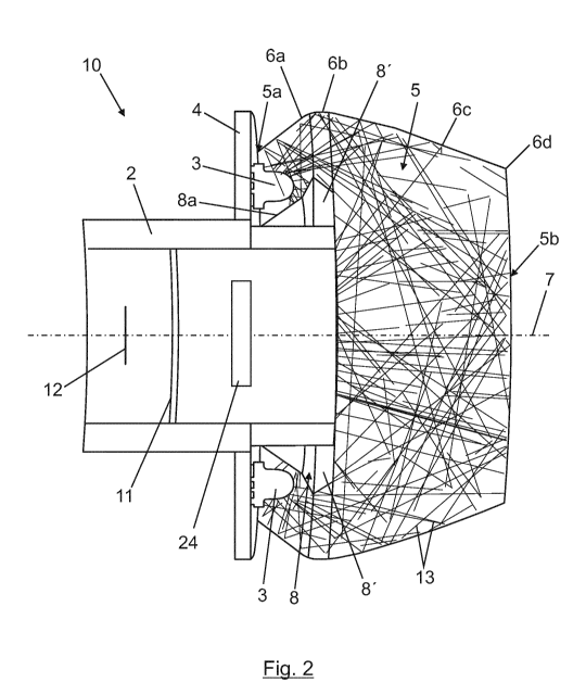
Figure 2 shows a sectional view of an optical system 10 comprising the
illumination
device 1 of Figure 1. The optical system 10 further includes optical means; in
particular,
an image sensor 12 for acquiring an image of the mark and a main lens 11
disposed in
front of the image sensor 12 to focus the light reflected from the mark onto
the image
sensor. In an embodiment, the illumination device 1 further includes a
luminescence filter
24 disposed inside the annular hollow body 2, in front of the main lens 11.
The
luminescence filter 24 is particularly useful when the illumination device 1
is used in a
luminescence reader (i.e. to read luminescent marks).
The external light reflector 5 is a hollow piece disposed concentrically to
the annular
hollow body 2. The internal wall 6 of the external light reflector 5 is made
of reflective
material to reflect the light (depicted as light rays 13) emitted from the
light source 3,
such as white plastic diffusive material or surface scattering metal to
enhance diffusion
of light. The special configuration and shape of the external light reflector
5 enhances
the redirection of light rays onto the zone at distal end 5b, where the mark
is to be placed,
achieving a more efficient and homogeneous illumination of the mark.
The internal wall 6 of the external light reflector 5 is a surface of
revolution with a specific
shape. In a first portion 6a of the internal wall 6, the cross section
progressively increases
along the axis of revolution (central axis 7) from a proximal end 5a of the
internal wall 6
of the external light reflector 5 to a first region 6b with maximum cross
section. The length
of the first region 6b along the central axis 7 may be very short, almost
infinitesimal, up
to a few millimeters. In a second portion 6c, the cross section of the
internal wall 6
CA 03065123 2019-11-27
WO 2018/224283 PCT/EP2018/062927
12
decreases continuously, reaching a second region 6d with minimum cross
section. In the
embodiment shown in Figure 2, the second region 6d is infinitesimal and
corresponds to
the distal end 5b. Alternatively, the second region 6d with minimum cross
section may
extend a short distance (e.g. a few millimeters) up to the distal end 5b. The
length of the
first portion 6a, or its projection on the central axis 7, is shorter than the
length or the
second portion 6c, or its projection on the central axis 7. This configuration
allows an
efficient and homogeneous redirection of the light rays 13 originating from
the light
source to the zone at the distal end 5b in a minimum volume, keeping the
device
compact.
The illumination device 1 further comprises a reflector element 8, the outer
surface 8a of
which is mirror-finished (e.g. polished aluminum or polished silver) and is at
least partly
facing the light source 3 such that part of the light originating from the
light source 3 is
reflected back towards the first portion 6a of the internal wall 6 of the
external light
reflector 5. This way, light incident onto the mark placed at the distal end
5b does not
impinge at angles such that a specular reflection from a flat mark or
substrate could be
imaged by the imaging system (main lens 11 and image sensor 12). This is
because the
light from the light source 3 does not travel directly up to the mark at
angles and areas
where a specular reflection would yield a hotspot in the imaging system, but
is instead
.. reflected and impinges on the mark/substrate at oblique angles. Thus, the
present
illumination device 1 avoids rays impinging onto the mark at angles which can
yield hot
spots in the imaging system.
According to an embodiment, the reflector element 8 comprises an opaque layer
8' on
.. the distal end of the reflector element 8 (i.e. the side of the reflector
element 8 closer to
the distal end 5b of the illumination device 1). The opaque layer 8' is
preferably made of
light diffusive material (e.g. implemented as a diffusive white part). The
opaque layer 8'
is used to increase light homogeneity and remove specular reflections on the
polished
outer surface of the reflector element 8. In the embodiment of Figure 2 the
reflector
.. element 8 and the layer 8' are coupled or fixed to the outer surface of the
annular hollow
body 2.
To increase security and prevent a user accidentally contacting the electronic
circuit of
the PCB 4 feeding the LEDs 3, a transparent layer 9 may be disposed
perpendicular to
the central axis 7, between the external light reflector 5 and the annular
hollow body 2
CA 03065123 2019-11-27
WO 2018/224283 PCT/EP2018/062927
13
(see Figure 1). The transparent layer 9 is preferably arranged within the
first region 6b
with maximum cross section. This way, the transparent layer 9 is annular-
shaped and
can be easily manufactured and assembled in the device. In an embodiment, the
transparent layer 9 is made of PMMA or polycarbonate.
Figure 3 illustrates a zoomed view of the reflector element 8, showing in more
detail the
redirection of light rays (13a, 13b) up to the first portion 6a of the
internal wall 6. In this
embodiment, the annular hollow body 2 is placed such that its distal end 2a
falls next to
or within the first region 6b of the external light reflector (5). In a
preferred embodiment,
the mirror finish outer surface 8a of the reflector element 8 is a surface of
revolution
arranged concentrically to the external light reflector 5. The reflector
element 8 shown in
Figure 3 is formed by two consecutive truncated cones (18a, 18b), it can be
funnel-
shaped with internal wall contour (i.e. generatrix) changing linearly along
central axis 7.
Figure 4 depicts another embodiment of the reflector element 8, with internal
wall
contour presenting generatrix shape having quadratic, cubic or in general
polynomial
dependency along central axis 7 (i.e. not only straight conical walls).
Moreover, the figure shows the specific design of the light scattering layer
8' which
prevents specular light reflection on the metallic back of the reflector
element 8 and thus
participates in the homogenization of the illumination and helps increasing
its efficiency.
The thickness and bevel angle 25 of the layer 8' can be optimized to avoid
shadowing of
light rays 13 which are reflected from the first portion 6a of the internal
wall 6 and are
directed to distal end 5b of the illumination device.
Figure 5 depicts another exemplary embodiment of the illumination device 1, in
which
the contour of the longitudinal section of the external light reflector 5 and
the reflector
element 8 is curved (and not linear, as in the embodiment of Figure 3). In
this particular
case, the increase of cross sections of the first portion 6a and of the mirror
finish outer
surface 8a is not linear (the cross sections of the second portion 6c are also
not linearly
decreasing). The shape of the curved section of the external light reflector 5
and/or the
reflector element 8 may be obtained using a computer-assisted optimization
process
including a ray model of light. The optimization process may be performed, as
shown in
the example of Figure 6, by establishing some fixed points 20 of the contour
and
computing additional variable points 21 of the contour that optimize the
reflection and
CA 03065123 2019-11-27
WO 2018/224283 PCT/EP2018/062927
14
light uniformity at the distal end 5b.
The optimization process includes:
- Varying the location of the variable points 21.
- Obtaining the value of parameters relating to a selection criterion
including at
least one of power, overall efficiency, and homogeneity of the light received
at a zone at the distal end 5b where the mark is placed. The homogeneity is
calculated according to the following equation:
Homogeneity ¨ Irrmin ______________________________ x100
Irrmax
where Irrmin and Irrmax are, respectively, the minimum and maximum irradiance
measured within the illuminated area defined by the distal end 5b. The image
of Figure 7 represents the normalized irradiance obtained in the optimization
process in the X and Y coordinates at the distal end 5b of the illumination
device where lines 23 show the ends of the area delimited by distal end 5b.
Figure 8 depicts a graph of the normalized irradiance along the X axis at a
central height (Y=0) for the illumination device of Figure 6, showing an
illumination homogeneity of 87,6%.
- Selecting the variable points 21 that maximize a function which considers
these parameters according to the selection criteria employed.
Some constraints may be employed in the optimization process; for instance,
fixing a
threshold for the minimum distance dmin between the light source 3 and the
reflector
element 8. In an embodiment, the minimum distance dm,n is at least 0.5 mm to
favor
reflection to the external light reflector S.
In order to generate a highly homogeneous light pattern at the distal end 5b,
the different
elements of the illumination device 1 (annular hollow body 2, light source 3,
external light
reflector 5 and reflector element 8) are arranged concentrically around the
central axis 7
(axis of revolution). The light source 3 may be formed by a plurality of light
emitting
sources, preferably LEDs, arranged symmetrically around the annular hollow
body 2.
The LEDs may be disposed on a ring-shaped PCB 4 concentric to the lens to
generate
uniform light in the plane where the mark is located. The annular hollow body
2 is
CA 03065123 2019-11-27
WO 2018/224283 PCT/EP2018/062927
preferably made of a light absorbing material, such as black plastic or
aluminum.
The present invention also refers to an optical system 10 for reading a
marking on an
object, such as the one shown in Figure 2. The optical system 10 comprises,
apart from
5 .. the illumination device 1, a light field acquisition device disposed
inside the annular
hollow body 2. In an embodiment, the light field acquisition device comprises
a main lens
11 and an image sensor 12 arranged in front of the main lens 11. The main lens
11
focuses light reflected back from the mark onto the image sensor 12. The
optical system
may be mounted on a widget attachable to a smartphone, or it may be mounted or
10 .. integrated in a handheld reader.
The present invention also relates to a reader apparatus for detecting a
marking on an
object. The apparatus, as shown in Figure 9A, comprises an optical system 10
including
the illumination device 1, and a processor for analyzing the image received
from the
15 .. optical system 10 to read, detect, decode and /or authenticate a mark.
The apparatus
may be a handheld reader, such as a smartphone or an optical scanner 30, as
depicted
in the example of Figure 9A. The optical system 10 mounted on an end of the
optical
scanner 30 is illustrated in detail in Figure 9B. The external light reflector
5 of the optical
system 10 is attached to an external housing 19, which may be part of the
optical system
10 itself or of the optical scanner 30.