Note: Descriptions are shown in the official language in which they were submitted.
CA 03065205 2019-11-27
- 1 -
Description
Title of Invention
FILTER DEVICE AND FILTER
Technical Field
[0001]
The present invention relates to a filter device in which a
filter and two waveguide tubes are coupled to each other. The
present invention also relates to a filter capable of being
coupled to the waveguide tubes.
Background Art
[0002]
As filters used in millimeter wave band, filters using a
waveguide tube made of a metal are widely known. Fig. 8 in
Non-Patent Literature 1 illustrates a filter which can be coupled
to a rectangular waveguide tube being rectangular in cross
section at opposite ends thereof. This filter includes a plurality
of resonators that are formed by cutting a metal block. At a
boundary between the adjacent resonators is provided a
coupling window for electromagnetically coupling the
resonators to each other. Such a filter constructed by coupling
a plurality of resonators to each other is called a resonator
CA 03065205 2019-11-27
- 2 -
coupled filter.
[0003]
The properties of this filter depend on a resonance
frequency of each resonator and a coupling coefficient between
the resonators. The resonance frequency is a physical quantity
which is determined by the size of each resonator, and the
coupling coefficient is a physical quantity which is determined
by the size of the coupling window. Accordingly, the properties
of the filter disclosed in Non-Patent Literature 1 strongly
depend on the size of the filter itself.
[0004]
Thus, in a case where the temperature of an external
environment changes, the properties of the filter disclosed in
Non-Patent Literature 1 vary according to the temperature
change. In other words, the filter disclosed in Non-Patent
Literature 1 is a highly temperature dependent filter. Variation
of the properties of the filter will cause transmission of
electromagnetic waves included in a band that are supposed to
be reflected. Thus, the filter disclosed in Non-Patent Literature
1 is not suitable for use in an environment in which the
temperature changes dramatically.
[00051
Examples of a filter having properties that are less
CA 03065205 2019-11-27
- 3 -
temperature dependent include a filter disclosed in Non-Patent
Literature 2. The filter disclosed in Non-Patent Literature 2 is a
resonator-coupled filter constituted by a post-wall waveguide
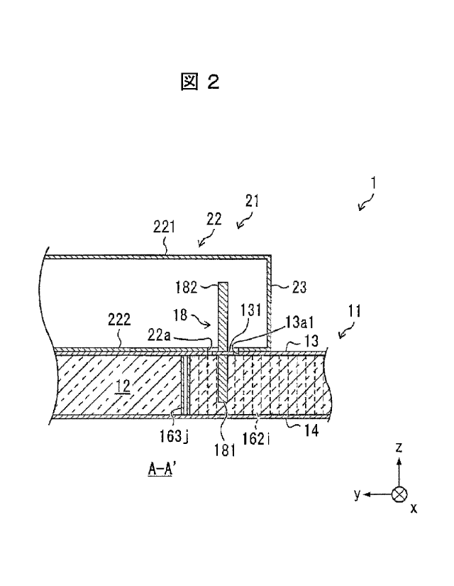
(PWW). In the PWW included in this filter, a region which is
rectangular in cross-sectional shape and is surrounded by a
pair of conductor layers provided on respective opposite
surfaces of a substrate made of a dielectric and by a post wall
constituted by a plurality of conductor posts which are placed
in the substrate in a fence-like manner, functions as a
propagation region through which electromagnetic waves
propagate.
[0006]
Note that since the substrate which is a constituent
member of the PWW is small in thickness, the width of the pair
of conductor layers in a cross section of the propagation region
is greater than the height of the post wall (equal to the
thickness of the substrate) in the cross section. Thus, in the
PWW, the pair of conductor layers is also called a pair of wide
walls, and the post wall is also called narrow walls. In a case
where directions parallel to a normal to the pair of wide walls
are referred to as upper and lower directions, directions
parallel to a direction of propagation of electromagnetic waves
are referred to as anterior and posterior directions, directions
CA 03065205 2019-11-27
- 4 -
orthogonal to the upper and lower directions and to the anterior
and posterior directions are referred to as left and right
directions, the pair of wide walls surrounds the propagation
region from the upper and lower directions, the narrow walls
surround the propagation region from the anterior and
posterior directions and from the left and right directions. Note
that, of all the narrow walls, narrow walls surrounding the
propagation region from the left and right directions are also
referred to as side walls, and narrow walls surrounding the
propagation region from the anterior and posterior directions
are also referred to as short walls.
[0007]
The filter disclosed in Non-Patent Literature 2 employs
quartz glass as a dielectric material constituting the substrate.
Quartz glass has a small linear expansion coefficient in
comparison with metal. Thus, in a case where the temperature
of the external environment greatly changes (in a case where
the temperature of the external environment changes in a range
of, for example, not less than -25 C and not more than 100 C),
the amount of change in size of the filter itself is small, as
compared to the filter disclosed in Non-Patent Literature 1.
Therefore, the properties of this filter have low temperature
dependence, as compared to the filter disclosed in Non-Patent
CA 03065205 2019-11-27
- 5 -
Literature 1.
Citation List
[Patent Literature]
[0008]
[Patent Literature 1]
Japanese Patent Application Publication Tokukai No.
2015-80100
[Patent Literature 2]
Japanese Patent Application Publication Tokukai No.
2015-226109
[Patent Literature 3]
Japanese Patent Application Publication Tokukai No.
2016-6918
[Non-patent Literature]
[0009]
[Non-patent Literature 1]
Kazuaki Yoshida, "Technology and Applications of
Microwave Filters", Japan Radio Co., Ltd. (JRC) Review No. 64,
December 2013.
[Non-patent Literature 2]
Y. Uemichi, et. al, "Compact and low-loss bandpass filter
realized in silica-based post-wall waveguide for 60-GHz
applications", IEEE MTT-S IMS, May 2015.
CA 03065205 2019-11-27
- 6 -
Summary of Invention
Technical Problem
[0010]
A filter is a passive device that limits a center frequency
and bandwidth of electromagnetic waves to be transmitted.
However, the coupling section between the filter and the
waveguide tube is required to reduce return loss over a wide
band. This is because the filter must limit a band of
electromagnetic waves, and it is not preferable that the
bandwidth is limited by the coupling section between the filter
and the waveguide tube.
[0011]
Unfortunately, the filter disclosed in Non-Patent
Literature 2, when connected with a waveguide tube, tends to
have large return loss, and it is thus difficult to broaden a
bandwidth in which reflection loss is small. This problem will
be described below.
[0012]
Patent Literatures 1 to 3 each disclose, as described
below, transmission lines in which a waveguide tube is coupled
to one end portion of the PWW. These transmission lines can be
used as a structure for coupling the filer and waveguide tube
CA 03065205 2019-11-27
- 7 -
disclosed in Non-Patent Literature 2 to each other.
[0013]
In the transmission line illustrated in Figs. 1 to 4 of
Patent Literature 1 (in Patent Literature 1, the transmission
line is described as "connection structure"), a coupling window
is provided by omitting a short wall of the PWW, and part of the
short wall of the waveguide tube is opened (in Patent Literature
1, the short wall is described as "closure structure"). In this
transmission line, the open part of the short wall in the
waveguide tube faces the coupling window of the PWW so that
the PWW and the waveguide tube are coupled to each other.
[0014]
In the transmission line illustrated in Figs. 1 to 3 of
Patent Literature 2 (in Patent Literature 2, the transmission
line is described as "transmission mode converting device"), the
PWW and the waveguide tube are placed in such a manner that
they share a conductor layer provided on one surface of the
substrate. This conductor layer functions as one wide wall of
the PWW and also functions as one wide wall of the waveguide
tube (see Fig. 3). To the wide wall shared by the PWW and the
waveguide tube are provided four rectangular coupling
windows. In this transmission line, the PWW and the waveguide
tube are coupled to each other via these four coupling windows.
CA 03065205 2019-11-27
- 8 -
[0015]
In the transmission line illustrated in Figs. 1 and 2 of
Patent Literature 3, a coupling window is provided in one wide
wall of the PWW, and a short wall of the waveguide tube is
opened. In this transmission line, a part of the wide wall where
the coupling window is provided in the PWW faces an open cross
section of the short wall of the waveguide tube so that the PWW
and the waveguide tube are coupled to each other.
[0016]
Further, the transmission lines disclosed in Patent
Literatures 1 to 3 employ a microstrip line (MSL) as a planar
transmission path to be coupled to an end portion of the PWW
on a side away from another end portion thereof on a side to
which the waveguide tube is connected, wherein the MSL
includes a signal line and a ground layer. Those transmission
lines include a columnar conductor (for example, in Patent
Literature 3, the columnar conductor is described as a power
feeding pin) that converts a mode of propagating through the
inside of the PWW into a mode of propagating through the inside
of the MSL. This columnar conductor couples the PWW and the
waveguide tube.
[00171
The above-described transmission lines as disclosed in
CA 03065205 2019-11-27
- 9 -
Patent Literatures 1 to 3, in a case where they are used as a
transmission line in which a filter and a waveguide tube are
coupled to each other, are required to have small return loss
(e.g., return loss of -15dB or less) over a wide band (e.g., in the
case of operation in the E-band, not less than 71 GHz to not
more than 86GHz).
[0018]
For example, in a case where -15 dB is set as a threshold
value against which to judge return loss, the bandwidths of all
of the transmission lines disclosed in Patent Literatures 1 to 3
are less than 10 GHz (see Fig. 9 of Patent Literature 1, Fig. 13
of Patent Literature 2, and Fig. 4 of Patent Literature 3). These
bandwidths are not sufficient for transmission lines in which a
filter and waveguide tubes are coupled to each other, and the
conventional transmission lines have room for broadening of
the band.
[00191
The present invention has been made in view of the above
problem, and it is an object of the present invention to broaden
a band in which return loss is small in a filter device including
(i) a filter using a PWW and (ii) waveguide tubes coupled to the
filter.
Solution to Problem
CA 03065205 2019-11-27
- 10 -
[0020]
In order to solve the above problem, a filter device in
accordance with an aspect of the present invention is a filter
device, including: a filter comprising a substrate made of a
dielectric, a pair of wide walls being constituted by a first
conductor layer and a second conductor layer, respectively, and
covering respective opposite surfaces of the substrate, and
narrow walls being constituted by post walls which are provided
inside the substrate; and a first waveguide tube and a second
waveguide tube each including a tube wall made of a conductor
and being placed along the substrate.
[0021]
The filter further includes: a first columnar conductor
passing through a first opening which is provided in the first
conductor layer, the first columnar conductor having one end
portion located inside the substrate; and a second columnar
conductor passing through a second opening which is provided
in the first conductor layer or the second conductor layer, the
second columnar conductor having one end portion located
inside the substrate.
[0022]
The first waveguide tube is placed such that the first
columnar conductor passes through an opening which is
CA 03065205 2019-11-27
- 11 -
provided in the tube wall of the first waveguide tube and such
that another end portion of the first columnar conductor is
located inside the first waveguide tube, and the second
waveguide tube is placed such that the second columnar
conductor passes through an opening which is provided in the
tube wall of the second waveguide tube and such that another
end portion of the second columnar conductor is located inside
the second waveguide tube.
[0023]
In order to solve the above problem, a filter in accordance
with an aspect of the present invention is a filter including: a
substrate made of a dielectric; a pair of wide walls being
constituted by a first conductor layer and a second conductor
layer, respectively, and covering respective opposite surfaces of
the substrate; and narrow walls being constituted by post walls
which are provided inside the substrate, the filter further
including: a first columnar conductor passing through a first
opening which is provided in the first conductor layer, the first
columnar conductor having one end portion located inside the
substrate; and a second columnar conductor passing through a
second opening which is provided in the first conductor layer or
the second conductor layer, the second columnar conductor
having one end portion located inside the substrate.
CA 03065205 2019-11-27
- 12 -
Advantageous Effects of Invention
[0024]
A filter device and a filter in accordance with an aspect of
the present invention can broaden a band in which return loss
is small.
Brief Description of Drawings
(0025]
Fig. 1 is an exploded perspective view illustrating part of
a filter device in accordance with Embodiment 1 of the present
invention.
Fig. 2 is a cross-sectional view illustrating a
PWW-waveguide tube converting section included in the filter
device illustrated in Fig. 1.
(a) of Fig. 3 is a cross-sectional view illustrating a
transmission line that includes a variation of a PWW-waveguide
tube converting section illustrated in Fig. 2. (b) of Fig. 3 is an
enlarged cross-sectional view illustrating the PWW-waveguide
tube converting section illustrated in (a) of Fig. 3.
(a) of Fig. 4 is a graph showing reflection characteristics
and transmission characteristics of a PWW-waveguide tube
converting section included in a filter device in Example 1 of the
present invention. (b) of Fig. 4 is a graph showing reflection
CA 03065205 2019-11-27
- 13 -
characteristics and transmission characteristics of a
PWW-waveguide tube converting section included in a filter
device in Example 2 of the present invention.
(a) and (b) of Fig. 5 are each a cross-sectional view
illustrating a filter device in accordance with Embodiment 2 of
the present invention.
Fig. 6 is a cross-sectional view illustrating Variation 1 of
the filter device illustrated in Fig. 5.
Fig. 7 is a cross-sectional view illustrating Variation 2 of
the filter device illustrated in Fig. 5.
Description of Embodiments
[0026]
A filter device in accordance with an aspect of the present
invention is a filter device obtained by coupling (i) a filter
constituted by a post-wall waveguide (PWW) and (ii) two
waveguide tubes (first waveguide tube and second waveguide
tube). In the filter device in accordance with an aspect of the
present invention, the filter is provided between the first
waveguide tube and the second waveguide tube.
[00271
A filter device in accordance with an aspect of the present
invention is designed to be operated in the E-band (band of not
CA 03065205 2019-11-27
- 14 -
less than 70 GHz to not more than 90 GHz). Further, a filter
device in accordance with an aspect of the present invention is
designed to be operated in an external environment with a
temperature of not less than -25 C and not more than 100 C.
[0028]
[Embodiment 1]
A filter device in accordance with Embodiment 1 of the
present invention will be described with reference to Figs. 1 and
2. Fig. 1 is an exploded perspective view illustrating a filter
device 1 in accordance with Embodiment 1. Fig. 2 is a
cross-sectional view illustrating a PWW-waveguide tube
converting section included in the filter device 1.
[0029]
In the filter device 1, a filter 11, a waveguide tube 21, and
a waveguide tube 31 are placed such that directions of
propagation of electromagnetic waves in the filter 11, the
waveguide tube 21, and the waveguide tube 31 are in line with
each other (preferably become parallel to each other). In
orthogonal coordinate systems illustrated in Figs. 1 and 2, a
y-axis is set to the directions of propagation of electromagnetic
waves in the filter 11, the waveguide tube 21, and the
waveguide tube 31, a z-axis is set to a direction normal to a
surface of a substrate 12, and an x-axis is set to a direction
CA 03065205 2019-11-27
- 15 -
orthogonal to the y-axis and the z-axis.
[0030]
Note that, in the present specification, in accordance
with the orientation of the filter device 1 arranged as illustrated
in Fig. 1, a z-axis positive (negative) direction is referred to as
an upper (lower) direction, an x-axis positive (negative)
direction is referred to as a left (right) direction, and a y-axis
positive (negative) direction is referred to as an anterior
(posterior) direction. Further, in a case where no specification
of whether a positive direction or a negative direction is made,
a z-axis direction is referred to as upper and lower directions,
an x-axis direction is referred to as left and right directions,
and a y-axis direction is referred to as anterior and posterior
directions.
[0031]
As illustrated in Fig. 1, the filter device 1 includes the
filter 11 constituted by a PWW, the waveguide tube 21, and the
waveguide tube 31. The waveguide tube 21 and the waveguide
tube 31 are a first waveguide tube and a second waveguide
tube, respectively, recited in the claims.
[0032]
(Filter 11)
The filter 11 is a laminate substrate in which a conductor
CA 03065205 2019-11-27
- 16 -
layer 13 and a conductor layer 14 are provided on opposite
sides of a substrate 12 made of a dielectric (made of quartz
glass in Embodiment 1). The conductor layer 13 and the
conductor layer 14 are, respectively, a first conductor layer and
a second conductor layer recited in the claims. Note that the
substrate 12 need only be made of a dielectric, and the
dielectric which constitutes the substrate 12 may be selected as
appropriate in consideration of at least one of a relative
dielectric constant, processability, and the like.
[0033]
The filter 11 has a first region R1 provided in advance in
the vicinity of an opening 13a1 (described later). In the first
region R1, part of a tube wall of the waveguide tube 21 can be
placed. Further, the filter 11 has a second region provided in
advance in the vicinity of an opening 13a2 (described later). In
the second region, part of a tube wall of the waveguide tube 31
can be placed. The opening 13a1 and the opening 13a2 are a
first opening and a second opening recited in the claims.
[0034]
Inside the substrate 12 are provided post walls obtained
by arranging a plurality of conductor posts 1611, 162i, 163j,
and 164j (where i and j are any positive integers) in a fence-like
manner (see Fig. 1).
CA 03065205 2019-11-27
- 17 -
[0035]
The plurality of conductor posts 161i, 162i, 163j, and
164j are obtained by charging a conductor such as a metal into
vias, which are formed so as to pass through the substrate 12
from the front surface to the rear surface of the substrate 12, or
by depositing the conductor on internal surfaces of the vias. All
of the plurality of conductor posts 161i, 1621, 163j, and 164j
electrically connect the conductor layer 13 and the conductor
layer 14. Note that a diameter of the conductor posts 161i, 162i,
163j, and 164j may be set as appropriate according to the
operation band. In Embodiment 1, the diameter of the
conductor posts 1611, 162i, 163j, and 164j is 100 pm. Further,
an interval between adjacent ones of the conductor posts 161i,
an interval between adjacent ones of the conductor posts 162i,
an interval between adjacent ones of the conductor posts 163j,
and an interval between adjacent ones of the conductor posts
164j are each 100 pm, which is equal to the diameter of the
conductor posts 1611, 162i, 163j, and 164j.
[0036]
A side wall 161, which is a post wall obtained by
arranging the plurality of conductor posts 1611 at a
predetermined spacial period in a fence-like manner, functions
as a kind of conductor wall that reflects electromagnetic waves
CA 03065205 2019-11-27
- 18 -
in a band corresponding to the spacial period.
[0037]
Similarly, a post wall obtained by the plurality of
conductor posts 162i constitutes a side wall 162, a post wall
obtained by the plurality of conductor posts 163j constitutes a
short wall 163, and a post wall obtained by the plurality of
conductor posts 164j constitutes a short wall 164. Further, the
side walls 161 and 162 and the short walls 163 and 164 are
collectively referred to as narrow walls 16. Individual plane
surfaces represented by imaginary lines (two-dot chain lines)
illustrated in Fig. 1 are imaginary plane surfaces each
including corresponding ones of central axes of the plurality of
conductor posts 161i, 162i, 163j, and 164j, and are plane
surfaces each schematically representing a conductor wall
which is imaginarily realized by a corresponding one of the side
walls 161 and 162 and the short walls 163 and 164.
[00381
Note that Fig. 1 omits some of the conductor posts 161i,
some of the conductor posts 162i, some of the conductor posts
163j, and some of the conductor posts 164j, for ease of viewing
of the configuration of the PWW-waveguide tube converting
section (described later).
[0039]
CA 03065205 2019-11-27
- 19 -
As illustrated in Fig. 1, the narrow walls 16 surround a
rectangular parallelepiped-shaped region from the anterior and
posterior directions and from the left and right directions.
Further, the conductor layer 13 and the conductor layer 14,
which are a pair of wide walls, surround the rectangular
parallelepiped-shaped region from the upper and lower
directions, respectively. Electromagnetic waves propagate
through a propagation region, i.e. the rectangular
parallelepiped-shaped region, in the y-axis direction of the
propagation region. Thus, the PWW is constituted by a pair of
wide walls and narrow walls.
10040]
In Embodiment 1, the above-described rectangular
parallelepiped-shaped propagation region is divided into a
resonator 11a, a resonator 11b, a resonator 11c, and a
resonator 11d by partition walls 171, 172, and 173. Note that,
as with the narrow walls 16, the partition walls 171, 172, and
173 are constituted by post walls.
[0041]
Although the partition wall 171 is constituted by the
conductor posts, no conductor posts are provided in and near a
center of the partition wall 171. Thus, the conductor posts are
not provided in some area of the post walls, and such an area
CA 03065205 2019-11-27
- 20 -
functions as a coupling window 171a through which the
resonator 1 la and the resonator 11b, adjacent to each other,
are electromagnetically coupled.
[0042]
Similarly, through a coupling window 172a provided in
and near the center of the partition wall 172, the resonator 11b
and the resonator 11c are coupled. Through a coupling window
173a provided in and near the center of the partition wall 173,
the resonator 11c and the resonator 1 id are coupled.
[0043]
The filter 11 configured by electromagnetically coupling
the resonators 11 a to II d in this manner is a resonator-coupled
filter.
[00441
(Waveguide tube 21)
The waveguide tube 21 is made of a conductor (in
Embodiment 1, a brass surfaced with gold plating). As
illustrated in Fig. 1, the waveguide tube 21 includes a tube wall
22, which is rectangular in cross section, and a short wall 23.
The short wall 23 seals an end portion (end portion on a y-axis
negative direction side) of the tube wall 22. That is, the
waveguide tube 21 is a rectangular waveguide tube. The tube
wall 22 has a wide wall 221 and a wide wall 222, which are a
CA 03065205 2019-11-27
- 21 -
pair of wide walls, and a narrow wall 223 and a narrow wall 224,
which are a pair of narrow walls.
[0045]
Out of the pair of wide walls, the wide wall 222 located on
a filter 11 side (on a z-axis negative direction side) has an
opening 22a, which is larger in diameter than a pin 18
(described later).
[0046]
To couple the filter 11 and the waveguide tube 21, the
waveguide tube 21 is brought close to the filter 11 in the z-axis
negative direction from a disassembled state illustrated in Fig.
1, and the waveguide tube 21 is placed on the filter 11 in such
a manner that the pin 18 passes through the opening 22a, and
a lower surface of the wide wall 222 comes into close contact
with an upper surface of the conductor layer 13 without any gap
between them.
[0047]
In the filter device 1 configured as described above, the
waveguide tube 21 is electromagnetically coupled to the filter
11 via the pin 18. Thus, the pin 18 is a PWW-waveguide tube
converting section through which the filter 11, which is
constituted by PWW, and the waveguide tube are coupled. The
PWW-waveguide tube converting section will be described in
CA 03065205 2019-11-27
- 22 -
detail later with reference to Fig. 2.
[0048]
In Embodiment 1, an end portion (end portion on a y-axis
positive direction side) of the waveguide tube 21 on a side
facing away from the short wall 23 is trimmed off so as to be
flush with an end face of the substrate 12 on the y-axis positive
direction side. However, the end portion of the waveguide tube
21 on the y-axis positive direction side may further extend
toward the y-axis positive direction side, without being trimmed
off. Further, as described later with reference to Fig. 7, the end
portion of the waveguide tube 21 on the y-axis positive direction
side may be coupled to a device, such as an antenna, which is
suitable to be coupled with use of a waveguide tube.
[0049]
Note that, in Embodiment 1, the waveguide tube 21 is left
hollow inside. Instead of having such a hollow structure, the
waveguide tube 21 may be configured such that dielectric
particles for adjusting a relative dielectric constant are charged
into the waveguide tube 21.
[0050]
(Waveguide tube 31)
The waveguide tube 31 has the same configuration as that
of the waveguide tube 21. That is, the waveguide tube 31 is
CA 03065205 2019-11-27
- 23 -
constituted by a tube wall 32 and a short wall 33. The tube wall
32 has a wide wall 321 and a wide wall 322, which are a pair of
wide walls, and a narrow wall 323 and a narrow wall 324, which
are a pair of narrow walls. Further, the wide wall 322 has an
opening 32a that is larger in diameter than a pin 19 (described
later).
[0051]
In the waveguide tube 21, the short wall 23 is placed on
the filter 11 so as to be located on the y-axis negative direction
side. In contrast, in the waveguide tube 31, the short wall 33 is
placed on the filter 11 so as to face in the direction opposite to
the direction in which the waveguide tube 21 faces, that is, so
as to be located on the y-axis positive direction side.
[0052]
The waveguide tube 31 is electromagnetically coupled to
the filter 11 via the pin 19. Thus, as in the case of the pin 18,
the pin 19 is a PWW-waveguide tube converting section. The
PWW-waveguide tube converting section will be described in
detail later with reference to Fig. 2.
[0053]
(PWW-waveguide tube converting section)
The filter device 1 includes a first PWW-waveguide tube
converting section, in which the filter 11 and the waveguide
CA 03065205 2019-11-27
- 24 -
tube 21 are coupled to each other, and a second
PWW-waveguide tube converting section, in which the filter 11
and the waveguide tube 31are coupled to each other. The first
PWW-waveguide tube converting section and the second
PWW-waveguide tube converting section have the same
configuration. Thus, in Embodiment 1, the PWW-waveguide
tube converting section included in the filter device 1 will be
described by taking the first PWW-waveguide tube converting
section as an example.
[0054]
A cross-sectional view of a cross section taken along line
A-A' in Fig. 1 (a cross section along a y-z plane surface) is
illustrated in Fig. 2. Fig. 2 is a cross-sectional view illustrating
the vicinity of the pin 18.
[0055]
As illustrated in Fig. 2, a portion of the conductor layer
13 is cut out in the shape of a ring in the vicinity of the
conductor posts 163j (conductor posts constituting the short
wall 163) in the propagation region of the filter 11. As a result,
the conductor layer 13 is provided with an opening 13a1. Inside
the opening 13a1 is provided a land 131 (not illustrated in Fig.
1) which is concentric with the opening 13a1. Further, a
circular opening is provided in and near the center of the land
CA 03065205 2019-11-27
- 25 -
131 (preferably in the center of the land 131), and the substrate
12 has a cylindrical pore which communicates with the circular
opening and extends from a surface of the substrate 12 (the
surface on a z-axis positive direction side) to the inside of the
substrate 12. As illustrated in Fig. 2, the pore is a
non-through-hole.
[0056]
The pin 18 (first columnar conductor recited in the
claims) made of a metal is secured to the substrate 12 by being
inserted into the opening and pore of the land 131 described
above. The pin 18 being inserted into the substrate 12 in this
way passes through the opening 13a1, and a lower end portion
181 of the pin 18 (one end portion recited in the claims) is
located inside the substrate 12, i.e. in the propagation region of
the filter 11. Further, an upper end portion 182 (another end
portion recited in the claims) of the pin 18 being secured in this
way is located inside the waveguide tube 21, i.e. in the
propagation region of the waveguide tube 21.
[0057]
The diameter of the pin 18, the length of the pin 18
(length along the z-axis direction), the length of a portion of the
pin 18 inserted into the substrate 12, and the length of a
portion of the pin 18 protruding through the surface of the
CA 03065205 2019-11-27
- 26 -
substrate 12 can be used as design parameters for optimizing
return loss. For example, in Embodiment 1, 180 pm is employed
as the diameter of the pin 18.
[0058]
Note that the end portion 182 of the pin 18 is not in
electrical communication with the wide wall 221. The length of
the portion of the pin 18 protruding through the substrate 12
can be adjusted within the bounds of the end portion 182 not
contacting the wide wall 221.
[0059]
In a case where electromagnetic waves propagating
through the propagation region of the filter 11 in the y-axis
positive direction are present, the portion of the pin 18 inserted
into the substrate 12 draws the electromagnetic waves which
have propagated through the propagation region of the filter 11,
and the portion of the pin 18 protruding through the substrate
12 radiates the electromagnetic waves into the propagation
region of the waveguide tube 21. Similarly, in a case where
electromagnetic waves propagating through the propagation
region of the waveguide tube 21 in the y-axis negative direction
are present, the portion of the pin 18 protruding through the
substrate 12 draws the electromagnetic waves from the
propagation region of the waveguide tube 21, and the portion of
CA 03065205 2019-11-27
- 27 -
the pin 18 inserted into the substrate 12 radiates the
electromagnetic waves into the propagation region of the filter
11. Thus, the pin 18 functions as the PWW-waveguide tube
converting section.
[0060]
As described above, the pin 18 electromagnetically
couples a mode of propagating through the propagation region
of the filter 11 and a mode of propagating through the
propagation region of the waveguide tube 21. The coupling
between the filter 11 and the waveguide tube 21 via the pin 18
is provided over a wide band, in comparison to coupling with
use of the conventional coupling window. Thus, the filter device
1 including the pin 18 can reduce return loss at a coupling
section between the filter 11 and the waveguide tube 21 over a
wide band, in comparison to the conventional transmission
device. Thus, the filter device 1 can broaden a band in which
return loss is small, in comparison to the conventional
transmission line.
[0061]
Note that, as described earlier, the filter 11 illustrated in
Figs. 1 and 2 can be easily coupled to the waveguide tube 21
and the waveguide tube 31 with use of (i) the waveguide tube 21
having the tube wall 22 with the opening 22a and (ii) the
CA 03065205 2019-11-27
- 28 -
waveguide tube 31 having the tube wall 32 with the opening
32a. Specifically, it is possible to couple the filter 11 and the
waveguide tube 21 by passing the pin 18 through the opening
22a provided in the waveguide tube 21 and by placing the
waveguide tube 21 such that the end portion 182 of the pin 18
is located inside the waveguide tube 21. The same applies to
coupling of the filter 11 and the waveguide tube 31
[0062]
A coupling section, provided in this way, between the
filter 11 and the waveguide tube 21 can reduce return loss over
a wide band. Similarly, a coupling section, provided in this way,
between the filter 11 and the waveguide tube 31 can reduce
return loss over a wide band. Thus, the filter 11 is also included
in the technical scope of the present invention.
[0063]
[Variation of pin 181
A pin 118, which is a variation of the pin 18, will be
described with reference to Fig. 3. (a) of Fig. 3 is a
cross-sectional view illustrating a filter device 1 including the
pin 118. (b) of Fig. 3 is an enlarged cross-sectional view
illustrating the pin 118. Note that, in Embodiment 1, a
variation is described by taking the pin 118 as an example.
However, as a matter of course, it is also possible to employ, as
CA 03065205 2019-11-27
- 29 -
a variation of the pin 19, the structure of the pin 118 obtained
by deforming the pin 18. In a case where the pin 118 is
employed as the first PWW-waveguide tube converting section
included in the filter device 1, it is preferable to employ a
variation of the pin 19 as the second PWW-waveguide tube
converting section.
[0064]
In the filter device 1 illustrated in Fig. 3, the pin 18
included in the filter device 1 illustrated in Figs. 1 and 2 is
replaced by the pin 118, and the waveguide tube 21 included in
the filter device 1 illustrated in Figs. 1 and 2 is replaced by a
waveguide tube 121. In the present variation, only different
features of the filter device 1 illustrated in Fig. 3, as compared
with the features of the filter device 1 illustrated in Figs. 1 and
2, will be described.
[0065]
The pin 118 is divided into a blind via 118a, which is a
first part, and a blind via 118b, which is a second part.
[0066]
The blind via 118a is configured as below. An opening
13a1 is provided in the vicinity of the conductor post 163j in the
propagation region of the filter 11. Inside the opening 13a1, a
land 131 is provided. Further, a cylindrical pore is provided in
CA 03065205 2019-11-27
- 30 -
and near the center of the land 131 (preferably in the center of
the land 131). The pore is a non-through-hole. The blind via
118a is obtained by charging a conductor such as a metal into
the non-through-hole or by depositing the conductor on an
internal surface of the non-through-hole. The blind via 118a
has a lower end portion (one end portion recited in the claims)
located inside the substrate 12, i.e. in the propagation region of
the filter 11. Further, the blind via 118a has an upper end
portion (another end portion recited in the claims) which is in
electrical communication with the land 131.
[0067]
The blind via 118b is embedded in a block 119 made of a
dielectric (made of quartz glass in Embodiment 1), an upper end
portion 118b1 (end portion on the z-axis positive direction side)
is located inside the block 119, and a lower end portion 118b2
(end portion on the z-axis negative direction side) reaches the
surface of the block 119.
[0068]
The blind via 118b can be produced as follows: A
substrate used as the block 119 is a substrate (i) having a
thickness smaller than a distance between the wide walls 1221
and 1222 of the waveguide tube 121, (ii) being made of a
dielectric (made of quartz glass in Embodiment 1), and (iii)
CA 03065205 2019-11-27
- 31 -
having a conductor layer 120 formed on one surface (surface on
the z-axis negative direction side in Fig. 3) of the substrate. A
plurality of blind vias are formed in a matrix manner on the
substrate having the conductor layer 120 formed thereon. Then,
by cutting the substrate having the plurality of blind vias
formed thereon into cubes, the block 119 having the blind via
118b formed thereon is obtained. Then, by cutting out a portion
of the conductor layer 120 in a ring shape, (i) a land 1201 which
is in electrical communication with the blind via 118b and (ii)
the conductor layer 120 surrounding the land 1201 while being
spaced away from the land 1201 are formed on the surface of
the block 119.
[0069]
As illustrated in (b) of Fig. 3, the land 1201 is connected
to the land 131 with use of a bump Bl. The conductor layer 120
is connected to the conductor layer 13 with use of bumps B2
and B3. The bumps B1 to B3, which are an aspect of an
electrically conductive connecting member, are each obtained
by forming a solder layer on a surface of a metallic spherical
member. In this manner, the blind via 118b is connected and
secured to the blind via 118a.
[0070]
Here, to reduce return loss as much as possible, it is
CA 03065205 2019-11-27
- 32 -
preferable that a central axis of the blind via 118a be coaxial
(coincide) with a central axis of the blind via 118b.
[0071]
The electrically conductive connecting member may be a
solder, an electrically conductive adhesive (e.g., silver paste),
or the like as an alternative to the bumps. However, by
employing the bumps B1 to B3 having a uniform diameter as the
electrically conductive connecting member, it is possible to
easily enhance parallelism between the surface of the substrate
12 on which the conductor layer 13 is formed and the surface of
the block 119 on which the conductor layer 120 is formed.
Thus, it is easy to connect the blind via 118a and the blind via
118b in a state in which the central axis of the blind via 118a
and the central axis of the blind via 118b are parallel to each
other.
[00721
In the case of the pin 18, a cylindrical pore having a
predetermined diameter (e.g., 180 pm) is provided in advance
on the substrate 12 at a predetermined position, and the pin 18
is inserted into the pore so that the pin 18 is secured to the
substrate 12. In this case, the diameter of the pore needs to be
precisely formed. The predetermined diameter is defined with a
certain margin (tolerance). However, in a case where the
CA 03065205 2019-11-27
- 33 -
diameter of a provided pore is smaller than the predetermined
diameter, the pin 18 cannot be inserted into the substrate. In a
case where the diameter of a provided pore is larger than the
predetermined diameter, the pin 18 cannot be firmly secured to
the substrate.
[0073]
Further, the pin 18, which is a very thin columnar
conductor, tends to bend when inserted into the pore.
Therefore, the operation of inserting the pin 18 into the
substrate 12 need to be done with a high degree of precision,
regardless of whether when a person carries out the operation
by hand or when a manipulator controlled by a machine is used
to carry out the operation.
[0074]
On the contrary, in the case of the pin 118, the blind via
118a and the blind via 118b can be connected easily and
accurately with use of the electrically conductive connecting
member such as the bumps B1 to B3. Thus, the filter device 1
with the pin 118 can be easily produced in comparison with the
filter device 1 with the pin 18.
[0075]
Further, the configuration in which the blind via 118b,
which is the second part, is embedded in the block 119 provides
CA 03065205 2019-11-27
- 34 -
ease of handling in comparison with a configuration in which
the second part is merely a columnar conductor (a
configuration in which the blind via 118b is not embedded in
the block 119). Thus, the filter device 1 with the pin 118 can be
produced more easily.
[00761
With the pin 118 embedded in the block 119, a size of an
opening 122a (see (a) of Fig. 3) provided on the wide wall 1222
of the waveguide tube 121 is larger than the opening 22a (see
Fig. 2). Specifically, when the filter device 1 is viewed in a plan
view, the size of the opening 122a is increased so as to
encompass the block 119. With such a configuration, the
waveguide tube 21 can be placed easily at a predetermined
position even when the pin 118 is embedded in the block 119.
[0077]
[Examples]
(Example 1)
As Example 1 of the present invention, reflection
characteristics and transmission characteristics were
calculated with use of the configuration of the PWW-waveguide
tube converting section included in the filter device 1
illustrated in Fig. 2. In Example 1, the pin 18 is employed as the
PWW-waveguide tube converting section. In Example 1, design
CA 03065205 2019-11-27
- 35 -
parameters of the pin 18 were determined as follows:
[0078]
Diameter: 180 pm
Length of the portion inserted into the substrate 12: 420
pm
Length of the portion protruding through the substrate
12: 700 pm
(Example 2)
As Example 2 of the present invention, reflection
characteristics and transmission characteristics were
calculated with use of the configuration of the PWW-waveguide
tube converting section included in the filter device 1
illustrated in Fig. 3. In Example 2, the pin 118 is employed as
the PWW-waveguide tube converting section.
[0079]
= Blind via 118a
Diameter: 100 pm
Length: 420 pm
= Blind via 118b
Diameter: 100 pm
Length: 700 pm
= Bumps B1 to B3
Diameter: 100 pm
CA 03065205 2019-11-27
- 36 -
(Common design parameters)
Note that the design parameters common to both Example
1 and Example 2 were determined as follows:
[0080]
= Filter 11
Thickness of the substrate 12: 520 pm
Dielectric constant of the substrate 12: 3.82
- Waveguide tube 21
Distance between the wide wall 221 and the wide wall
222: 1149 pm
Distance between the narrow wall 223 and the narrow
wall 224: 2500 pm
(Reflection characteristics and
transmission
characteristics)
(a) of Fig. 4 is a graph showing reflection characteristics
(frequency dependence of S11) and transmission
characteristics (frequency dependence of S21) in Example 1. (b)
of Fig. 4 is a graph showing reflection characteristics
(frequency dependence of S11) and transmission
characteristics (frequency dependence of S parameter S21) in
Example 2. In both (a) of Fig. 4 and (b) of Fig. 4, the symbol
"S11" is given to a plot of the reflection characteristic, and the
symbol "S21" is given to a plot of the transmission
CA 03065205 2019-11-27
- 37 -
characteristics.
[0081]
Referring to (a) of Fig. 4, the reflection characteristics,
S11, in Example 1 is not more than -15 dB in a band of
approximately not less than 71 GHz to not more than 88 GHz.
[0082]
Referring to (b) of Fig. 4, the reflection characteristics,
S11, in Example 2 is not more than -15 dB in a band of
approximately not less than 73 GHz to not more than 90 GHz.
[0083]
As described above, the transmission lines in Examples 1
and 2 achieved reduction of return loss over a wide band, in
comparison to the transmission line provided with the
conventional PWW-waveguide tube converting section with use
of a coupling window.
[0084]
Further, both Example 1 and Example 2, with return loss
reduced over a wide band, exhibit favorable transmission
characteristics over a wide band.
[0085]
The second PWW-waveguide tube converting section has
the same configuration as that of the first PWW-waveguide tube
converting section. Thus, the second PWW-waveguide tube
CA 03065205 2019-11-27
- 38 -
converting section shows the same results as those shown in
the Examples described above.
[0086]
[Embodiment 21
A filter device in accordance with Embodiment 2 of the
present invention will be described with reference to Fig. 5. (a)
and (b) of Fig. 5 are each a cross-sectional view illustrating a
filter device 401 in accordance with Embodiment 2. (a) of Fig. 5
illustrates a cross-sectional view taking along a plane surface
(y-z plane surface) that (i) includes a central axis of a pin 418,
which is a columnar conductor constituting the
PWW-waveguide tube converting section, and (ii) extends along
a direction (y-axis direction) of propagation of electromagnetic
waves. (b) of Fig. 5 illustrates a cross-sectional view taken
along a plane surface (z-x plane surface) that (i) includes the
central axis of the pin 418 and (ii) intersects the direction
(y-axis direction) of propagation of electromagnetic waves.
[0087]
As illustrated in Fig. 5, the filter device 401 includes a
filter 411, a housing 441, and a resin substrate 451.
[0088]
(Filter 411)
The filter 411 has the same configuration as that of the
CA 03065205 2019-11-27
- 39 -
filter 11 illustrated in Figs. 1 and 2. Corresponding constituent
members of the filter 411 have reference symbols which are
obtained by putting "4" in front of reference symbols of the
constituent members of the filter 11. In Embodiment 2,
descriptions of those constituent members will be omitted.
[00891
(Housing 441)
The housing 441 illustrated in Fig. 5 is made by forming,
in a rectangular parallelepiped-shaped metal block, tubular
spaces 4211 and 4311 rectangular in cross section and a recess
4411 for accommodating the filter 411. The tubular space 4211
and the tubular space 4311 correspond to the first tubular
space and the second tubular space recited in the claims,
respectively.
(00901
In Fig. 5, the housing 441 is placed on a resin substrate
451 (described later) such that a lengthwise direction of the
metal block coincides with a y-axis direction of an orthogonal
coordinate system illustrated in Fig. 5, and a height direction of
the metal block coincides with a z-axis direction of the
orthogonal coordinate system illustrated in Fig. 5.
(00911
Out of six side wall surfaces constituting the metal block,
CA 03065205 2019-11-27
- 40 -
a z-x plane surface on a y-axis positive direction side has the
rectangular parallelepiped-shaped tubular space 4211 which is
dug in the y-axis negative direction. Further, out of the six side
wall surfaces constituting the metal block, a z-x plane surface
on a y-axis negative direction side has the rectangular
parallelepiped-shaped tubular space 4311 which is dug in the
y-axis positive direction. These tubular spaces 4211 and 4311
function as waveguide tubes 421 and 431 that guide
electromagnetic waves in the y-axis direction, respectively, in
the same manner as the waveguide tubes 21 and 31 illustrated
in Figs. 1 and 2.
[0092]
In other words, as illustrated in (a) and (b) of Fig. 5, an
upper wall 4221, a lower wall 4222, a right wall 4223, and a left
wall 4224, all of which surround the sides of the tubular space
4211, constitute a tube wall 422 of the waveguide tube 421. Out
of the walls defining the tubular space 4211, the wall along the
z-x plane surface constitutes a short wall 423 of the waveguide
tube 421. Thus, the upper wall 4221 and the lower wall 4222
form a wide wall of the waveguide tube 421. The right wall 4223,
the left wall 4224, and the short wall 423 form a narrow wall of
the waveguide tube 421.
[0093]
CA 03065205 2019-11-27
- 41 -
The tubular space 4311 is constituted in the same
manner as the tubular space 4211 and is defined by a tube wall
432 and a short wall 433. The tube wall 432 is constituted by an
upper wall 4321 and a lower wall 4322, which are a pair of wide
walls, and a right wall 4323 and a left wall 4324, which are a
pair of narrow walls. In the state illustrated in (a) of Fig. 5, the
tubular space 4311 is provided so as to be mirror symmetric to
the tubular space 4211 about a symmetry axis (axis parallel to
a z-axis). A distance between the short wall 423 and the short
wall 433 is set according to a distance between the pin 418 and
the pin 419. Then, the tubular space 4311 is provided such that
the above-described symmetry axis coincides with an imaginary
line which is a set of points equidistant from the pin 418 and
the pin 419.
[0094)
Out of six side wall surfaces constituting the metal block,
an x-y plane surface on a z-axis negative direction side has the
rectangular parallelepiped-shaped recess 4411 which is dug in
the z-axis positive direction. The shape of an opening of the
recess 4411 corresponds to the shape of the substrate 412 of
the filter 411. To allow the recess 4411 to accommodate the
filter 411, the filter 411 is pushed into the recess 4411 through
the opening of the recess 4411 in the z-axis positive direction.
CA 03065205 2019-11-27
- 42 -
Note that the recess 4411 is provided at a position so as to be
mirror symmetric about a symmetry axis (axis parallel to the
z-axis). The symmetry axis about which the recess 4411 is
mirror symmetric coincides with the symmetry axis about which
the tubular space 4211 and the tubular space 4311 are mirror
symmetric.
[0095]
Note that a rim of the housing 441 around the recess 4411
is referred to as a skirt 4412. To reliably accommodate the filter
411, the depth of the recess 4411, i.e. the height of the skirt
4412, is set to be greater than the thickness of the filter 411
(total thickness of the substrate 412, the conductor layer 413,
and the conductor layer 414).
(0096]
As illustrated in (a) and (b) of Fig. 5, an opening 421a is
provided at a boundary between a region of the tubular space
4211 on the y-axis negative direction side of the lower wall
4222, which is one of the members defining the tubular space
4211, and a region of the bottom surface of the recess 4411 on
the y-axis positive direction side. The tubular space 4211 and
the recess 4411 communicate with each other via the opening
421a.
[00971
CA 03065205 2019-11-27
- 43 -
Similarly, an opening 431a is provided at the boundary
between the tubular space 4311 and the recess 4411. The
tubular space 4311 and the recess 4411 communicate with each
other via the opening 431a.
[0098]
The filter 411 is placed inside the recess 4411 such that
(1) an end portion of the pin 418, which is the first
PWW-waveguide tube converting section, on the z-axis positive
direction side is located inside the tubular space 4211, and the
conductor layer 413 seals the opening 421a and such that (2) an
end portion of the pin 419, which is the second PWW-waveguide
tube converting section, on the z-axis positive direction side is
located inside the tubular space 4311, and the conductor layer
413 seals the opening 431a. Thus, in the region in which the
opening 421a is provided, a portion of the conductor layer 413
that seals the opening 421a functions as a portion of the lower
wall 4222 of the waveguide tube 421. Further, in the region in
which the opening 431a is provided, a portion of the conductor
layer 413 that seals the opening 431a functions as a portion of
the lower wall 4322 of the waveguide tube 431.
[00991
According to this configuration, the pin 418 can
electromagnetically couple a mode of propagating through the
CA 03065205 2019-11-27
- 44 -
waveguide tube 421 and a mode of propagating through the
filter 411. Since the opening 421a is sealed by the conductor
layer 413, loss does not increase. Similarly, the pin 419 can
electromagnetically couple a mode of propagating through the
waveguide tube 431 and a mode of propagating through the
filter 411. Since the opening 431a is sealed by the conductor
layer 413, loss does not increase.
(0100)
Further, the housing 441 is configured such that the
whole of the filter 411 is accommodated inside the recess 4411.
Therefore, the housing 441 can reliably protect the filter 411 (in
particular, substrate 412) against an external impact.
(01011
Note that as illustrated in Fig. 5, the waveguide tube 421
may be coupled to another waveguide tube, i.e. a waveguide
tube 461, on an open end side of the waveguide tube 421. The
waveguide tube 431 may be coupled to another waveguide tube,
i.e. a waveguide tube 471, on an open end side of the waveguide
tube 431. In Embodiment 2, a flange 442 is provided on the
open end side of the waveguide tube 421. Further, a flange 463
is provided at the end portion of the waveguide tube 461 on the
waveguide tube 421 side. The flange 442 and the flange 463 are
secured with use of a bolt 481 and a nut 482, so that the
CA 03065205 2019-11-27
- 45 -
waveguide tube 421 and the waveguide tube 461 are coupled to
each other. The same applies to a flange 443, which is provided
on an open end side of the waveguide tube 431, and a flange
473, which is included in the waveguide tube 471.
[0102]
(Resin substrate 451)
The resin substrate 451 is configured such that the resin
substrate 451 is capable of holding the filter 411 in a state in
which the filter 411 is sandwiched between the resin substrate
451 and the housing 441. As illustrated in (b) of Fig. 5, the
housing 441 and the resin substrate 451 are secured with use
of bolts 483 and 485 and nuts 484 and 486. A combination of
the bolt 483 and the nut 484 and a combination of the bolt 485
and the nut 486 are each an aspect of a pressure applying
member recited in the claims. The pressure applying member is
not limited to a combination of a bolt and a nut.
[0103]
The resin substrate 451 is made of resin (made of glass
epoxy resin in Embodiment 2). A resin material constituting the
resin substrate 451 can be selected as appropriate in view of
thermal expansion properties, processability, and the like.
[0104]
On a surface of the resin substrate 451 on a side facing
CA 03065205 2019-11-27
- 46 -
the filter 411 (on the z-axis positive direction side), is provided
a protrusion in a shape corresponding to the recess 4411 (in a
shape corresponding to a skirt 4412). This protrusion pushes
the filter 411 toward the housing 441 (to the z-axis positive
direction side).
[0105]
At this time, the height of the skirt 4412 of the housing
441 is so set that the skirt 4412 and the resin substrate 451 are
spaced away from each other.
[0106]
According to the above configuration, the protrusion of
the resin substrate 451 pushes the conductor layer 414 of the
filter 411 in the z-axis positive direction. As a result, the
conductor layer 413 of the filter 411 is pushed onto the bottom
surface of the recess 4411 of the housing 441. That is, the
surface of the conductor layer 413 and the bottom surface of
the recess 4411 are in close contact with each other, and thus
prevent generation of an air gap in an interface IF.
[01071
Thus, the housing 441 and the resin substrate 451 are
secured in a state in which the surface of the conductor layer
413 and the bottom surface of the recess 4411 are in close
contact with each other without any gap between them.
CA 03065205 2019-11-27
- 47 -
[0108]
With the above configuration, the filter 411 is sandwiched
between the housing 441 and the resin substrate 451. This
prevents the filter 411 from being displaced inside the recess
4411. In this way, the filter 411 and the waveguide tube 421 can
be reliably held in proper positions in relation to each other,
and the filter 411 and the waveguide tube 431 can be reliably
held in proper positions in relation to each other. Thus, it is
possible to prevent fluctuation of return loss that can occur at
a coupling section between the filter 411 and the waveguide
tube 421 and at a coupling section between the filter 411 and
the waveguide tube 431. Thus, the filter device 401 can reliably
broaden a band in which return loss is small, in comparison to
the conventional transmission line.
[0109]
Further, since it is possible to prevent generation of an
air gap in the interface IF, it is possible to prevent
electromagnetic waves propagating through the waveguide tube
421 and electromagnetic waves propagating through the
waveguide tube 431 from entering the interface IF. Thus, it is
possible to further reduce loss that can occur at the coupling
section between the filter 411 and the waveguide tube 421 and
at the coupling section between the filter 411 and the
CA 03065205 2019-11-27
- 48 -
waveguide tube 431.
[0110]
Further, according to the above configuration, the
waveguide tube 421 is integrally molded with the housing 441,
and the filter 411 is firmly secured to the recess 4411 of the
housing 441. Thus, the filter device 401 allows the waveguide
tube 421 and the waveguide tube 431 to be firmly coupled to the
filter 411.
[0111]
[Variation 1]
A filter device 501, which is Variation 1 of the filter device
401, will be described with reference to Fig. 6. Corresponding
constituent members of the filter device 501 in common with
the filter device 401 have reference symbols which are obtained
by replacing the initial number "4" of reference symbols for the
filter device 401 (see Fig. 5) by "5". In the present variation,
only different features of the filter device 501, as compared with
the features of the filter device 401, will be described, and the
other features will be omitted.
[0112]
As illustrated in Fig. 6, a resin substrate 551 included in
the filter device 501 has no protrusion provided thereon,
although the resin substrate 451 has the protrusion provided
CA 03065205 2019-11-27
- 49 -
thereon. That is, a surface of the resin substrate 551 on the
side facing the housing 541 is constituted by a flat surface.
[0113]
A skirt 5412 is configured such that the height of the
skirt 5412 is greater than the thickness of the filter 511 (total
thickness of a substrate 512, a conductor layer 513, and a
conductor layer 514). This allows the conductor layer 514 and
the resin substrate 551 to be spaced away from each other. That
is, the conductor layer 514 and the resin substrate 551 have an
air gap between them. In this way, the filter device 501 has an
air gap between the conductor layer 514 and the resin substrate
551. Thus, in an area where the air gap is present, a protrusion
(protrusion of the resin substrate 451) may be provided on the
surface of the resin substrate 551 on a side facing the housing
541
[0114]
In the present embodiment, a resin material is filled in
the air gap. Examples of the resin material include an adhesive,
a resin mold, and the like. These resin materials are viscous
fluids when filled, and then cures into a solid after a lapse of a
predetermined time period.
[0115]
For example, assume that a resin material in an amount
CA 03065205 2019-11-27
- 50 -
exceeding the volume of the above-described air gap is filled in
the air gap. In this case, the resin material thus filled is raised
above the air gap by surface tension. In this state, the curing
reaction of the resin material is proceeded. Then, at a point in
time when the resin material becomes semi-cured, the resin
substrate 551 is secured to the housing 541. According to this
configuration, the resin material having a volume which
exceeds the volume of the air gap causes a pressure for pushing
the filter 511 toward the housing 541 (to the z-axis positive
direction). Thus, according to this configuration, it is possible
to prevent generation of an air gap in an interface IF between
the surface of the conductor layer 513 and the bottom surface
of the recess 5411, with use of a simple configuration.
[0116]
[Variation 2]
A filter device 601, which is Variation 2 of the filter device
401, will be described with reference to Fig. 7. Corresponding
constituent members of the filter device 601 in common with
the filter device 401 have reference symbols which are obtained
by replacing the initial number "4" of reference symbols for the
filter device 401 (see Fig. 5) by "6". In the present variation,
only different features of the filter device 601, as compared with
the features of the filter device 401, will be described, and the
CA 03065205 2019-11-27
- 51 -
other features will be omitted.
[0117]
As illustrated in Fig. 7, a resin substrate 651 included in
the filter device 601 has a protrusion which is provided on the
resin substrate 451. On the surface of the protrusion, a
conductor layer 652 is provided.
[0118]
A skirt 6412 is configured such that the height of the
skirt 6412 is less than a sum of (a) the thickness of a filter 611
(total thickness of a substrate 612, a conductor layer 613, and
a conductor layer 614), (b) the height of the resin substrate
651, and (c) the thickness of the conductor layer 652. This
allows the skirt 6412 and the resin substrate 651 to be spaced
away from each other. That is, the skirt 6412 and the resin
substrate 651 have an air gap between them. Thus, as long as
the skirt 6412 and the resin substrate 651 have the air gap
between them, the surface of the resin substrate 651 on a side
facing the housing 641 may be flat.
[0119]
Besides, the conductor layer 614 of the filter 611 is
connected to the conductor layer 652 by use of a plurality of
bumps DB. The bumps DB are an aspect of the connecting
members recited in the claims, each of the bumps DB connects
CA 03065205 2019-11-27
- 52 -
the conductor layer 652 and the conductor layer 614 with each
other in its dot-like narrow region.
[0120]
In this way, the filter 611 and the resin substrate 651
may be connected to each other by use of a plurality of
connecting members. According to such a configuration, it is
possible to firmly secure the filter 611 to the resin substrate
651.
[0121]
Aspects of the present invention can also be expressed as
follows:
A filter device (1, 401, 501, 601) in accordance with an
embodiment of the present invention is a filter device (1, 401,
501, 601), including: a filter (11, 411, 511, 611) including a
substrate (12, 412, 512, 612) made of a dielectric, a pair of wide
walls being constituted by a first conductor layer (13, 413, 513,
613) and a second conductor layer (14, 414, 514, 614),
respectively, and covering respective opposite surfaces of the
substrate (12, 412, 512, 612), and narrow walls being
constituted by post walls which are provided inside the
substrate (12, 412, 512, 612); and a first waveguide tube (21,
121, 421, 521, 621) and a second waveguide tube (31, 431) each
including a tube wall (22, 32, 122, 422, 432, 522, 622) made of
CA 03065205 2019-11-27
- 53 -
a conductor and being placed along the substrate (12, 412, 512,
612).
[01221
The filter (11, 411, 511, 611) further includes: a first
columnar conductor (18, 118, 418, 518, 618) passing through a
first opening (13a1) which is provided in the first conductor
layer (13, 413, 513, 613), the first columnar conductor (18,
118, 418, 518, 618) having one end portion (181, 118a1) located
inside the substrate (12, 412, 512, 612); and a second columnar
conductor (19, 419) passing through a second opening (13a2)
which is provided in the first conductor layer (13, 413, 513,
613) or the second conductor layer (14, 414, 514, 614), the
second columnar conductor (19, 419) having one end portion
(191) located inside the substrate (12, 412, 512, 612).
[0123]
The first waveguide tube (21, 121, 421, 521, 621) is
placed such that the first columnar conductor (18, 118, 418,
518, 618) passes through an opening (22a, 122a) which is
provided in the tube wall (22, 122, 422, 522, 622) of the first
waveguide tube (21, 121, 421, 521, 621) and such that another
end portion (182, 118b1) of the first columnar conductor (18,
118, 418, 518, 618) is located inside the first waveguide tube
(21, 121, 421, 521, 621), and the second waveguide tube (31,
CA 03065205 2019-11-27
- 54 -
431) is placed such that the second columnar conductor (19,
419) passes through an opening (32a) which is provided in the
tube wall (32, 432) of the second waveguide tube (31, 431) and
such that another end portion (192) of the second columnar
conductor (19, 419) is located inside the second waveguide tube
(31, 431).
[0124]
According to the above configuration, the filter and the
first waveguide tube are electromagnetically coupled to each
other via the first columnar conductor passing through the first
opening which is provided in the first conductor layer.
Similarly, the filter and the second waveguide tube are
electromagnetically coupled to each other via the second
columnar conductor passing through the second opening which
is provided in the first conductor layer or the second conductor
layer.
[0125]
The first columnar conductor and the second columnar
conductor can reduce return loss at a coupling section between
the filter and the waveguide tube over a wide band, in
comparison to a coupling window which couples a filter and a
waveguide tube in the conventional transmission device. Thus,
the filter device in accordance with an embodiment of the
CA 03065205 2019-11-27
- 55 -
present invention can broaden a band in which return loss is
small, in comparison to a case where a filter and a waveguide
tube are coupled to each other with use of the conventional
transmission line.
[0126]
Further, a filter device (1, 401, 501, 601) in accordance
with an embodiment of the present invention is preferably
configured such that the filter (11, 411, 511, 611) further
includes one or more partition walls (171, 172, 173) being
constituted by post walls provided inside the substrate (12,
412, 512, 612) and dividing a region surrounded by the pair of
wide walls (13, 14, 413, 414, 513, 514, 613, 614) and the
narrow walls into a plurality of resonators (11a to 11d), the one
or more partition walls (171, 172, 173) having respective
coupling windows (171a, 172a, 173a).
[0127]
Further, a filter device (1) in accordance with an
embodiment of the present invention is preferably configured
such that the first columnar conductor (118) and the second
columnar conductor are each divided into a first part (118a)
and a second part (118b), the first part (118a) being embedded
in the substrate (12) and having one end portion (118a2) which
reaches a surface of the substrate (12), the second part (118b)
CA 03065205 2019-11-27
- 56 -
protruding through the substrate (12), and the first part (118a)
and the second part (118b) are connected to each other by an
electrically conductive connecting member (B1).
[0128]
Each of the columnar conductors of the transmission line
in accordance with an embodiment of the present invention is
divided into the first part and the second part, as described
above. The first part, which is embedded in the substrate and
has one end portion exposed to the surface of the substrate, can
be formed by a method similar to a method of forming the post
wall. Then, by connecting the second part to the first part with
use of the electrically conductive connecting member, each of
the columnar conductors is formed.
[0129]
A transmission line in accordance with an embodiment of
the present invention can be produced by such a production
method. Thus, the transmission line in accordance with an
embodiment of the present invention can be produced easily, in
comparison with a transmission line including a columnar
conductor which is constituted by a single member.
[0130]
Further, a filter device (1) in accordance with an
embodiment of the present invention is preferably configured
CA 03065205 2019-11-27
- 57 -
such that the second part (118b) of each of the first columnar
conductor (118) and the second columnar conductor is
embedded in a block (119) made of a dielectric, and an end
portion (118b2) of the second part on a side facing the first part
(118a) reaches a surface of the block (119).
[0131]
The above configuration allows the second part to be
easily handled in connecting the second part to the first part.
Thus, the transmission line in accordance with an embodiment
of the present invention can be produced more easily, in
comparison with a transmission line in which the second part is
not embedded in the block.
[0132]
Further, a filter device (401, 501, 601) in accordance with
an embodiment of the present invention further includes: a
housing (441, 541, 641) made of a metal, the housing including
a first tubular space (4211), a second tubular space (4311), and
a recess (4411, 5411, 6411), the first tubular space (4211)
functioning as a propagation region of the first waveguide tube
(421, 521, 621), the second tubular space (4311) functioning as
a propagation region of the second waveguide tube (431), the
recess (4411, 5411, 6411) accommodating the filter (411, 511,
611); and a resin substrate (451, 551, 651) holding the filter
CA 03065205 2019-11-27
- 58 -
(411, 511, 611) in a state in which the filter (411, 511, 611) is
sandwiched between the resin substrate (451, 551, 651) and the
housing (441, 541, 641).
[0133]
In the filter (411, 511, 611), the second opening provided
in the first conductor layer (413, 513, 613) or the second
conductor layer (414, 514, 614) is provided in the first
conductor layer (413, 513, 613).
[0134]
The recess (4411, 5411, 6411) and the first tubular space
(4211) communicate with each other via a first opening which is
provided at a boundary between the recess (4411, 5411, 6411)
and the first tubular space (4211), and the recess (4411, 5411,
6411) and the second tubular space (4311) communicate with
each other via a second opening which is provided at a
boundary between the recess (4411, 5411, 6411) and the
second tubular space (4311).
[0135]
The filter (411, 511, 611) is preferably placed such that
the another end portion of the first columnar conductor (418,
518, 618) and the another end portion of the second columnar
conductor (419) are located inside the first tubular space
(4211) and the second tubular space (4311), respectively, and
CA 03065205 2019-11-27
- 59 -
such that the first conductor layer (413, 513, 613) seals the
first opening and the second opening which are provided at the
boundaries.
[0136]
According the above configuration, the filter is
sandwiched with use of the housing and the resin substrate.
Thus, the filter and the waveguide tube can be reliably held in
positions in relation to each other. Thus, it is possible to
prevent fluctuation of return loss that can occur at a coupling
section between the filter and the waveguide tube. Thus, the
filter device in accordance with an embodiment of the present
invention can reliably broaden a band in which return loss is
small, in comparison to a case where a filter and a waveguide
tube are coupled to each other with use of the conventional
transmission line.
[0137]
Further, a filter device (401, 601) in accordance with an
embodiment of the present invention further includes a
pressure applying member (483, 484, 485, 486, 683, 684, 685,
686) which applies pressure to a skirt (4412, 6412), which is a
rim of the housing (441, 641) around the recess (4411, 6411),
and to the resin substrate (451, 651) in such a direction that
the filter (411, 611) is sandwiched between the skirt (4412,
CA 03065205 2019-11-27
- 60 -
6412) and the resin substrate (451, 651).
[0138]
It is preferable that a height of the skirt (4412, 6412) is so
set that the skirt (4412, 6412) and the resin substrate (451,
651) are spaced away from each other.
[0139]
According the above configuration, in connecting the
resin substrate and the housing to each other, pressure is
applied to the resin substrate and the housing in such a
direction that the filter is sandwiched between the resin
substrate and the housing. By so setting the height of the skirt
that the skirt and the resin substrate are spaced away from
each other, the filter is pushed in such a direction that the
filter approaches the housing. Thus, it is possible to prevent
generation of an air gap in between the first conductor layer of
the filter and the recess of the housing.
[0140]
Further, a filter device (501) in accordance with an
embodiment of the present invention further includes a
pressure applying member (583, 584, 585, 586) which applies
pressure to a skirt (5412), which is a rim of the housing (541)
around the recess (5411), and to the resin substrate (551) in
such a direction that the filter (511) is sandwiched between the
CA 03065205 2019-11-27
- 61 -
skirt (5412) and the resin substrate (551).
[0141]
It is preferable that a height of the skirt (5412) is so set
that the second conductor layer (514) of the filter (511) and the
resin substrate (551) are spaced away from each other, and a
resin material is filled in an air gap between the second
conductor layer (514) and the resin substrate (551).
[0142]
By filling the resin substrate in the air gap between the second
conductor layer of the filter and the resin substrate, the resin
material pushes the filter in such a direction that the filter
approaches the housing. Thus, it is possible to prevent
generation of an air gap in between the first conductor layer of
the filter and the recess of the housing.
[0143]
Further, a filter device (601) in accordance with an
embodiment of the present invention further includes a
pressure applying member (683, 684, 685, 686) which applies
pressure to a skirt (6412), which is a rim of the housing (641)
around the recess (6411), and to the resin substrate (651) in
such a direction that the filter (611) is sandwiched between the
skirt (6412) and the resin substrate (651).
[0144]
CA 03065205 2019-11-27
- 62 -
It is preferable that a height of the skirt (6412) is so set
that the second conductor layer (614) of the filter (611) and the
resin substrate (651) are spaced away from each other, and the
second conductor layer (614) is connected to the resin
substrate (651) by a plurality of connecting members (DB).
[0145]
In this way, the filter and the resin substrate may be
connected to each other by a plurality of connecting members.
According to such a configuration, it is possible to firmly secure
the filter to the resin substrate.
[0146]
A filter (11, 411, 511, 611) in accordance with an
embodiment of the present invention is a filter including: a
substrate (12, 412, 512, 612) made of a dielectric; a pair of wide
walls (13,14,413,414,513,514,613,614) being constituted by a
first conductor layer (13, 413, 513, 613) and a second
conductor layer (14, 414, 514, 614), respectively, and covering
respective opposite surfaces of the substrate (12, 412, 512,
612); and narrow walls being constituted by post walls which
are provided inside the substrate (12, 412, 512, 612), the filter
(11, 411, 511, 611) further including: a first columnar
conductor (18, 118, 418, 518, 618) passing through a first
opening (13a1) which is provided in the first conductor layer
CA 03065205 2019-11-27
- 63 -
(13, 413, 513, 613), the first columnar conductor (18, 118, 418,
518, 618) having one end portion (181, 118a1) located inside
the substrate (12, 412, 512, 612); and a second columnar
conductor (19, 419) passing through a second opening (13a2)
which is provided in the first conductor layer (13, 413, 513,
613) or the second conductor layer (14, 414, 514, 614), the
second columnar conductor (19, 419) having one end portion
(191) located inside the substrate (12, 412, 512, 612).
[0147]
According to the above configuration, with use of the first
waveguide tube and the second waveguide tube each having the
tube wall provided with the opening, it is possible to easily
couple the filter and these waveguide tubes to each other.
Specifically, it is possible to easily couple the filter and the first
and second waveguide tubes to each other by (1) placing the
first waveguide tube such that the first columnar conductor
passes through the first opening which is provided in the tube
wall of the first waveguide tube and such that another end
portion of the first columnar conductor is located inside the
first waveguide tube and by (2) placing the second waveguide
tube such that the second columnar conductor passes through
the second opening which is provided in the tube wall of the
second waveguide tube and such that another end portion of the
CA 03065205 2019-11-27
- 64 -
second columnar conductor is located inside the second
waveguide tube.
[0148]
The coupling sections, provided in this way, between the
filter and the waveguide tubes can reduce return loss over a
wide bandwidth, as in the case of the filter device in accordance
with an embodiment of the present invention.
[0149]
Further, a filter (11, 411, 511, 611) in accordance with an
embodiment of the present invention is preferably configured
such that the first conductor layer (13, 413, 513, 613) has a
first region (R1) provided in advance in a vicinity of the first
opening (13a1), the first region (R1) allowing part of the tube
wall (22, 122, 422, 522, 622) of the first waveguide tube (21,
121, 421, 521, 621) to be placed in the first region (R1), and the
first conductor layer (13, 413, 513, 613) or the second
conductor layer (14, 414, 514, 614) has a second region
provided in advance in a vicinity of the second opening (13a2),
the second region allowing part of the tube wall (32, 432) of the
second waveguide tube (31, 431) to be placed in the second
region.
[0150]
Further, it is preferable that a filter (11, 411, 511, 611) in
CA 03065205 2019-11-27
- 65 -
accordance with an embodiment of the present invention
further includes one or more partition walls (171, 172, 173)
being constituted by post walls provided inside the substrate
(12, 412, 512, 612) and dividing a region surrounded by the
pair of wide walls (13, 14, 413, 414, 513, 514, 613, 614) and the
narrow walls into a plurality of resonators (11a to 11d), the one
or more partition walls (171, 172, 173) having respective
coupling windows (171a, 172a, 173a).
[0151]
Note that in the above section starting with "Aspects of
the present invention can also be expressed as follows:", only
members whose reference symbols are indicated in Figs. 1 to 7
out of the members corresponding to the constituent
components recited in the claims, are followed by their
reference symbols in parentheses.
[0152]
The present invention is not limited to the embodiments,
but can be altered by a skilled person in the art within the
scope of the claims. The present invention also encompasses, in
its technical scope, any embodiment derived by combining
technical means disclosed in differing embodiments.
Reference Signs List
CA 03065205 2019-11-27
- 66 -
[0153]
1, 401, 501, 601: Filter device
11, 411, 511, 611: Filter
12, 412, 512, 612: Substrate
13, 413, 513, 613: Conductor layer (first conductor layer,
wide wall)
14, 414, 514, 614: Conductor layer (second conductor
layer, wide wall)
16: Narrow wall
161, 162: Side wall
161i, 162i: Conductor post
163, 164: Short wall
171, 172, 173: Partition wall
171a, 172a, 173a: Coupling window
18, 19, 118, 418, 419, 518, 618: Pin (columnar
conductor)
181, 182, 191, 192, 118a1, 118b1: End portion of the pin
118a, 118b: Blind via
119: Block
120: Conductor layer
1201: Land
Bl, B2, B3: Bump
21, 31, 421, 431, 521, 621: Waveguide tube
CA 03065205 2019-11-27
- 67 -
22, 32, 122, 422, 432, 522, 622: Tube wall
221, 222, 321, 322, 4221, 4222, 4321, 4322, 5221, 6221:
Wide wall
223, 224, 4223, 4224, 5223, 5224, 6223, 6224: Narrow
wall
23, 33, 423, 433: Short wall
441, 541, 641: Housing
4411, 5411, 6411: Recess
451, 551, 651: Resin substrate