Note: Descriptions are shown in the official language in which they were submitted.
CA 03065371 2019-11-28
WO 2018/227246 PCT/AU2018/050586
- 1 -
QUALITY CONTROL OF SUBSTRATE COATINGS
Field of the Invention
[0001] The present invention relates to devices and methods for detecting the
amount of
material coating a medical device or substrate, in particular the present
invention relates to
devices and methods for detecting the amount of vaccine material coating a
microarray patch.
Background of the Invention
[0002] Medical devices may be coated with any number of biocompatible
materials.
Therapeutic drugs, agents or compounds may be mixed with the biocompatible
materials and
affixed to at least a portion of the medical device. These therapeutic drugs,
agents or
compounds may be utilized to promote healing deliver drugs and provide pain
relief. Various
materials and coating methodologies may be utilized to maintain the drugs,
agents or
compounds on the medical device until delivered and positioned. Medical
devices that may be
coated with various compounds include stents, grafts, anastomotic devices,
perivascular
wraps, sutures, staples and microprojection arrays. Microprojection arrays or
micro array
patches (MAPS) are an effective way of delivering therapeutic agents or
biomarkers to
patients as the patches induce minimal or no pain, induce little or no injury
from the
microneedles and reduce the possibility of cross infection. The solid
projections or needles on
a patch can be coated with drugs or macromolecules. These can be subsequently
delivered to a
desired target by the penetration of the projections or needles into the skin.
The
microprojections can be coated by the therapeutic agents using a variety of
techniques such as
dip coating, spray coating, gas jet drying, electrodynamic atomization and ink
jet printing.
[0003] Regardless of the methods used for coating the microprojections on the
arrays it is
useful to assess the amount of material coating the target delivery region of
the
microprojections which is often the upper 1/2 to 1/4 of the microprojections.
Several different
techniques have been applied in an attempt to quantify the amount of material
coated onto the
microprojections. One technique provides for dissolving the coating and
quantifying the
active material by high-performance liquid chromatography (Ma, et al. J. Pharm
Sci. 2014
103(11): 3621-3630. Other techniques to determine the loading of material
onto
CA 03065371 2019-11-28
WO 2018/227246 PCT/AU2018/050586
- 2 -
microprojection arrays include determining the residual amount of material
either on the
microprojections after use or on the skin after the microprojection array has
been removed.
Fluorescence microscopy can detect fluorescent materials on the
microprojections or in the
skin after the microprojection array has been removed. Scanning electron
microscopy can be
used to take images of the microprojections before and after coating. These
techniques usually
require destruction of the coating and/or are cumbersome and slow. There
exists a need to
assess each microprojection array at high speed in an aseptic manufacturing
environment to
determine that the dose and position of the coated material, such as a
vaccine, on the
projections is correct. Preferably, the method for assessing the dose and
position of the coated
material would not destroy the coating in the process.
[0004] As the dried vaccine on the microprojections appears optically "clear",
the use of
standard imaging techniques to establish contrast between the coating and the
polymer is not
straightforward. Furthermore, it is desirable to determine if the upper
portions of the
microprojections are coated as this is the portion of the microprojection that
enters the skin to
deliver the material to the subject. Coating of the lower portions of the
microprojections
and/or the base upon which the microprojections rest is a waste of valuable
biological
material. The determination of the loading of the coating should be performed
in an aseptic,
non-destructive and rapid fashion.
[0005] The reference in this specification to any prior publication (or
information derived
from it), or to any matter which is known, is not, and should not be taken as
an
acknowledgment or admission or any form of suggestion that the prior
publication (or
information derived from it) or known matter forms part of the common general
knowledge in
the field of endeavor to which this specification relates.
Summary of the Invention
[0006] The present invention relates to devices and methods for detecting the
amount of
material coating a medical device or substrate. In particular, the devices and
methods of the
present invention are able to detect the amount of vaccine material coating a
microarray patch.
Uncoated substrate surfaces (e.g. polymers) may have different reflectance
and/or a
fluorescence emission spectrum from a coated substrate when the substrate is
irradiated with a
CA 03065371 2019-11-28
WO 2018/227246 PCT/AU2018/050586
- 3 -
radiation source. Often, the reflectance or fluorescence signal is reduced
when the substrate is
coated versus the uncoated substrate.
[0007] The devices and methods of the present invention enable the use of
electromagnetic
radiation directed onto an uncoated/coated microprojection array or micro
array patch (MAP)
to be reflected off the array or to induce an electromagnetic emission and
detected to
determine the extent of coating of the microprojections on the microprojection
arrays. The use
of a laser (or other illumination source with appropriate illumination
filters), and an intensity
sensor (with appropriately chosen collection filters) to measure the reflected
or emitted
intensity of the electromagnetic radiation from a coated MAP correlates with
coating
performance or transfer efficiency of the coating onto the microprojections.
[0008] Inkjet coating is an emerging technology that can aseptically coat
biologics onto
MAP' s. High speed reflectance measurement(s) allows a quantifiable value to
ascertain
whether the coating on the projection meets specification in terms of the mass
of coated
material and its position on the patch relative to base.
[0009] In one broad form, an aspect of the present invention seeks to provide
a method for
determining the amount (degree, extent) of coating on microprojections of a
coated
microprojection array, the method comprising: irradiating an uncoated
microprojection array
with an electromagnetic radiation source; measuring the reflected radiation
from the uncoated
microprojection array; irradiating an uncoated microprojection array with an
electromagnetic
radiation source; measuring the reflected radiation from the uncoated
microprojection array;
and determining the extent of coating on the microprojections by comparing the
reflected
radiation from the uncoated microprojection array to that of the coated
microprojection array.
[0010] In one embodiment, the measuring of the reflected radiation from the
uncoated
microprojection array and the measuring of the reflected radiation from the
coated
microprojection array is done simultaneously.
[0011] In one embodiment, the measuring of the reflected radiation from the
uncoated
microprojection array and the measuring of the reflected radiation from the
coated
microprojection array is done sequentially.
CA 03065371 2019-11-28
WO 2018/227246 PCT/AU2018/050586
- 4 -
[0012] In another broad form, an aspect of the present invention seeks to
provide a method for
determining the amount of coating on the microprojections of a coated
microprojection array,
the microprojection array comprising a base from which the microprojections
project, the
method comprising: irradiating the coated microprojection array with a light
source;
measuring the reflected radiation from the base of the coated microprojection
array; and
determining the amount of coating on the microprojections by comparing the
reflected
radiation from the coated microprojection array to that of an uncoated
microprojection array.
[0013] In one embodiment, the reflected radiation is measured by a sensor.
[0014] In one embodiment, the number of sensors is four.
[0015] In one embodiment, the sensors are at approximately 45 degree downward
angle to the
microprojections and at 45 degrees out of alignment with the rows of
microprojections.
[0016] In one embodiment, the electromagnetic radiation source is
substantially perpendicular
to the microprojection array.
[0017] In one embodiment, the electromagnetic radiation source is at an angle
relative to the
microprojection array.
[0018] In one embodiment, the electromagnetic radiation source is aligned over
the
microprojection array such that the angle relative to the microprojections is
less than 5 .
[0019] In one embodiment, the electromagnetic radiation source is aligned over
the
microprojection array such that the angle relative to the microprojections is
less than about
20 .
[0020] In one embodiment, the electromagnetic radiation source is aligned over
the
microprojection array such that the angle relative to the microprojections is
less than about
45 .
[0021] In another broad form, an aspect of the present invention seeks to
provide a device for
measuring the coating on the microprojections on a microprojection array, the
device
comprising: an electromagnetic radiation source for illuminating the
microprojection array; a
CA 03065371 2019-11-28
WO 2018/227246 PCT/AU2018/050586
- 5 -
microprojection array housing for mounting the microprojection array; and one
or more
sensors for detecting reflected radiation from the microprojection array.
[0022] In one embodiment, the radiation source is a laser diode.
[0023] In one embodiment, the radiation source is a laser diode which emits
radiation from
about 200nm to 10000nm.
[0024] In one embodiment, the radiation source is a laser diode which emits
radiation at
635nm.
[0025] In one embodiment, the sensor is a silicon photodiode.
[0026] In one embodiment, the silicon photodiode has a detection range of 200
to 1100nm.
[0027] In one embodiment, the device is confined in an aseptic housing.
[0028] In one embodiment, the device further comprises a reference sensor.
[0029] In one embodiment, the number of sensors is four.
[0030] In one embodiment, the sensors are at approximately 45 degree downward
angle to the
microprojections and at 45 degrees out of alignment with the rows of
microprojections.
[0031] In one embodiment, the electromagnetic radiation source is
substantially perpendicular
to the microprojection array.
[0032] In one embodiment, the electromagnetic radiation source is aligned over
the
microprojection array such that the angle relative to the microprojections is
less than 50
.
[0033] In another broad form, an aspect of the present invention seeks to
provide a device for
measuring the coating on the microprojections on a microprojection array, the
device
comprising: a laser diode for illuminating the microprojection array; an
aspheric lens; a beam
shaping diffuser; a focusing lens wherein the aspheric lens is positioned
between the laser
diode and the beam shaping diffuser and the beam shaping diffuser is
positioned between the
aspheric lens and the focusing lens and the focusing lens is positioned
between the beam
CA 03065371 2019-11-28
WO 2018/227246 PCT/AU2018/050586
- 6 -
shaping filter and the microprojection array housing; microprojection array
housing for
mounting a microprojection array; a bi-convex lens; a sensor for detecting
reflected light from
the microprojection array wherein the biconvex lens is positioned between the
microprojection
array housing and the receiver; and a power meter connected to the sensor.
[0034] In one embodiment, the device further comprises a microarray mounting
station.
[0035] In one embodiment, the device further comprises one or more
microarrays.
[0036] In one embodiment, the laser diode emits electromagnetic radiation at
bout 635nm.
[0037] In one embodiment, the device further comprises an aperture positioned
between the
focusing lens and the microprojection array housing.
[0038] In one embodiment, the device further comprises a mirror positioned
between the
aperture and the microprojection array housing
[0039] In one embodiment, the device further comprises a reference sensor.
[0040] In one embodiment, the number of sensors is four.
[0041] In one embodiment, the sensors are at approximately 45 degree downward
angle to the
microprojections and at 45 degrees out of alignment with the rows of
microprojections.
[0042] In one embodiment, the laser diode is substantially perpendicular to
the
microprojection array.
[0043] In one embodiment, the laser diode is aligned over the microprojection
array such that
the angle relative to the microprojections is less than 50
.
[0044] In another broad form, an aspect of the present invention seeks to
provide a method for
determining the extent (degree, amount) of coating on microprojections of a
coated
microprojection array comprising: irradiating an uncoated microprojection
array with an
electromagnetic radiation source; measuring the emitted radiation from the
uncoated
microprojection array; irradiating a coated microprojection array with a light
source;
measuring the emitted radiation from the coated microprojection array; and
determining the
CA 03065371 2019-11-28
WO 2018/227246 PCT/AU2018/050586
- 7 -
extent of coating on the microprojections by comparing the emitted radiation
from the
uncoated microprojection array to that of the coated microprojection array.
[0045] In one embodiment, the emitted radiation is fluorescence.
[0046] In one embodiment, the electromagnetic radiation source emits at
approximately
445nm.
[0047] In one embodiment, the fluorescence is detected by a sensor with a
filter having a
bandpass of between about 455nm to 515nm.
[0048] In another broad form, an aspect of the present invention seeks to
provide a method for
determining the extent (degree, amount) of coating on a substrate comprising:
irradiating an
uncoated microprojection array with a first electromagnetic radiation source
which reflects off
the substrate and a second electromagnetic radiation source which promotes
fluorescence in
either the substrate or the coating or both; measuring the reflected radiation
from the uncoated
microprojection array; measuring the emitted fluorescence radiation from the
uncoated
microprojection array; irradiating a coated microprojection array with a first
electromagnetic
radiation source which reflects off the substrate and a second electromagnetic
radiation source
which promotes fluorescence in either the substrate or the coating or both
irradiating a coated
microprojection array with a light source; measuring the reflected radiation
from the coated
microprojection array; measuring the emitted fluorescence radiation from the
coated
microprojection array; and determining the extent of coating on the
microprojections by
comparing the reflected radiation from the uncoated microprojection array to
that of the coated
microprojection array and by comparing the reflected radiation from the
uncoated
microprojection array to that of the coated microprojection array.
[0049] In another broad form, an aspect of the present invention seeks to
provide a method for
controlling the quality of coated microprojection arrays, the method
including: determining the
amount (degree, extent) of coating on microprojections of a coated
microprojection array
using the method as described above; comparing the determined amount of
coating to a
coating specification; and rejecting the coated microprojection array if the
determined amount
of coating is outside of the coating specification.
CA 03065371 2019-11-28
WO 2018/227246 PCT/AU2018/050586
- 8 -
[0050] In another broad form, an aspect of the present invention seeks to
provide a system for
controlling the quality of coated microprojection arrays, the system including
a device as
described above that determines the amount of coating on microprojections of a
coated
microprojection array; and a processing system configured to: receive, from
the device, an
indication of the determined amount of coating; compare the determined amount
of coating to
a coating specification; and determine that the coated microprojection array
should be rejected
if the determined amount of coating is outside of the coating specification.
[0051] It will be appreciated that the broad forms of the invention and their
respective features
can be used in conjunction, interchangeably and/or independently, and
reference to separate
broad forms is not intended to be limiting.
Brief Description of the Drawings
[0052] Various examples and embodiments of the present invention will now be
described
with reference to the accompanying drawings, in which: -
[0053] . Figure lA is a schematic diagram of a side view of the
microprojection array and the
relative position of the detector and illumination source relative to the
microprojection array;
Figure 1B is the image the detector would see given the orientation of the
detector in
accordance with Figure 1A.
[0054] Figure 2A is a schematic diagram of a side view of the microprojection
array and the
relative position of the detector at a 45 degree angle to the microprojection
array; Figure 2B is
a schematic diagram of an overhead view of the detector direction relative to
the
microprojection array and the direction of the detector for detecting
reflectance; Figure 2C is
the image the detector would see given the orientation of the detector in
accordance with
Figures 2A and 2B; Figure 2D is a schematic diagram of a side view of the
microprojection
array and the relative position of the detector at a 45 degree angle to the
microprojection array;
Figure 2E is a schematic diagram of an overhead view of the detector direction
relative to the
microprojection array and the direction of the detector for detecting
reflectance; Figure 2F is
the image the detector would see given the orientation of the detector in
accordance with
Figures 2D and 2E; Figure 3 is a schematic diagram of an overhead view of a
microprojection
CA 03065371 2019-11-28
WO 2018/227246 PCT/AU2018/050586
- 9 -
array where the radiation illumination is from the top with little or no angle
and the use of four
detectors at approximately 45 degree downward angle and at 45 degrees out of
alignment with
the rows of microprojections.
[0055] Figures 4A-4D are schematic diagrams of an illumination scheme
respectively, large
spot reflectance, linear dot array, line scan array and two dimensional array.
[0056] Figure 5A is a fluorescence image of dried vaccine on a flat polymer
disc, to
demonstrate the principle of fluorescence reduction. The excitation wavelength
is set at 445nm
and the emission filter is 455-530nm. The polymer surface fluoresces when
excited with 445
nm light, and the dried vaccine reduces the measured intensity; Figure 5B is a
photograph of a
polymer microprojection array coated with dried vaccine where the excitation
wavelength is
set at 405nm and the emission filter is 495-515nm. In this scenario, the dried
vaccine does not
appear to significantly reduce the fluorescence intensity of the underlying
polymer. These
conditions could potentially serve as a reference measurement that would be
similar to an
uncoated patch.
[0057] Figure 6A-6C present data from FTIR scans of flat polymer discs with
dried vaccine
for the purpose of potentially identifying useful spectral features. Figure 6A
is the spectra
obtained from the polymer without dried vaccine. Figures 6B and 6C are data
from different
regions within the dried vaccine drop (edge of dried drop, and center of dried
drop). Spectral
features in the wavenumber range from 1300 cm-1 to 1900 cm-1 are highlighted
that seem to
correlate with the presence of dried vaccine.
[0058] Figure 7 is a schematic diagram of one embodiment of the equipment
setup for
reflectance detection of a coating on a substrate
[0059] Figure 8A is a drawing of one embodiment of the equipment setup for
detecting the
coating on a coated substrate; and Figure 8B is a drawing of an alternate
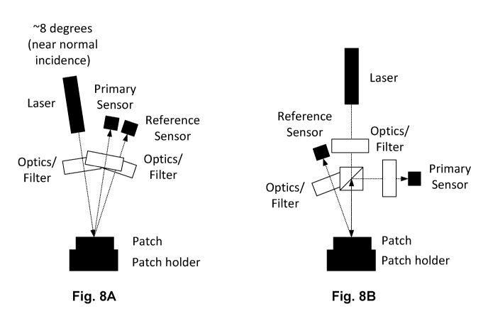
embodiment of the
equipment setup for detecting the coating.
[0060] Figure 9 is a schematic diagram of one embodiment of the equipment
setup for
detecting the coating on a coated substrate.
CA 03065371 2019-11-28
WO 2018/227246 PCT/AU2018/050586
- 10 -
[0061] Figure 10 is a schematic diagram of one embodiment of the laser diode
housing.
[0062] Figure 11 is a schematic diagram of one embodiment of the receiver
housing.
[0063] Figure 12 is a schematic diagram of one embodiment of the patch mount.
[0064] Figure 13 is a plot of normalized reflectance versus coating transfer
efficiency.
[0065] Figure 14 is a schematic diagram of one embodiment of the housing of
the device.
[0066] Figure 15 is a schematic diagram of one embodiment of the device as
viewed through
the housing of the device.
[0067] Figure 16 is a schematic diagram of one embodiment of the device as
viewed through
the top of the housing of the device.
[0068] Figure 17A is a schematic diagram of one embodiment of the device as
viewed through
the side of the housing of the device; Figure 17B is a schematic diagram of
one embodiment
of the device without the housing.
[0069] Figure 18A is a plot of low dose total protein transfer ( g) versus
laser reflectance (%);
Figure 19B is a plot of high dose total protein transfer ( g) versus laser
reflectance (%).
[0070] Figure 19 is a table of laser acceptance criteria for low dose and high
dose amounts.
[0071] Figure 20A is a schematic of the coating percentages by quadrant for a
microprojection
array; Figure 20B is a "heat map" representation of reflectance vs position
data of the coating
of the microprojection array. Green color represents a high intensity (i.e.
Significant tip
coating) and red color is mapped to low intensity readings (i.e. With
significant base coating).
[0072] Figure 21A is top-down view of an illustrated example of a patch mat;
Figure 21B is a
side-view of an illustrated example of a patch mat.
[0073] Figure 22 is a schematic diagram of one embodiment of a quality control
station where
a mat of patches may be coated by multiple print heads and then conveyed to a
quality control
CA 03065371 2019-11-28
WO 2018/227246 PCT/AU2018/050586
- 11 -
station where the patches can be checked for amount and position of coating on
the
microprojections.
[0074] Figure 23 is a schematic of one system that provides feedback
information so that the
coating of the MAPs performed by the print heads can be monitored and adjusted
based on the
data.
Detailed Description of the Invention
[0075] The present invention relates to devices and methods for detecting the
amount of
material coating a medical device or substrate, in particular the present
invention relates to
devices and methods for detecting the amount of vaccine material coating a
microarray patch
in real time.
[0076] The patches take a variety of forms from metal formed patches to
polymer molded
patches to patch projections formed from the vaccine or pharmacological
solution itself. The
manufacture of these patches relies on the ability to deposit a dried down
drug solution or
vaccine onto the tips of the microprojections with high throughput and high
accuracy.
Accurately coating the projections is important as the delivery of the coated
material to the
patient needs to be consistent. If too little material is delivered the
efficacy of the treatment is
compromised. Too much material could lead to overdosing or at a minimum
wasting
expensive vaccine or drug. The ability to coat the patches quickly is
necessary to producing a
commercial product. Coating of a Micro Array Patch (MAP) and other vaccine and
biologic
platforms requires the precise dosing and allocation of biologics targeting
each individual
projection on the platform with a controlled dose. Typically, a MAP (Micro
Array Patch)
platform has a length and a width of less than 20 mm and carries an evenly
spaced two-
dimensional array of projections. The microprojections are situated on a
substantially planar
base. The number of projections in either dimension may be less than 100.
Therefore the
projection density on the MAP is usually between 2,000 and 10,000 per cm2. The
total amount
of pharmaceutical formulation such as a vaccine required to coat each
projection is typically
more than 500 picolitres and must be accurately measured both in terms of the
applied dried
volume of material and the position of the material on the microprojection.
For example it
would be informative to determine whether the material deposited on the
microprojections was
CA 03065371 2019-11-28
WO 2018/227246 PCT/AU2018/050586
- 12 -
located on the top fourth of the microprojection or top half of the
microprojection or whether
the entire microprojection was coated. Furthermore, in order to accomplish
large volume
manufacturing of MAPs, each patch may need to be coated with one or more drops
(e.g. 1-6
drops per microprojection or between 20p1 to 1 L of material) in in a short
time period (e.g.
seconds). It is important to be able to quantify the amount of material that
is distributed onto
the microprojections in a manner that is preferably non-destructive and which
does not contact
the material or the microprojections. The method should be rapid enough to
keep up with
production levels of microprojection arrays which could number in the millions
per week.
The devices and methods of the present invention provide the ability to
determine the amount
of material coated onto the microprojections of the MAP.
[0077] The devices and methods of the present invention can determine the
amount of
material deposited on a substrate where the substrate is made of both an area
that is nominally
"to be coated" and an area that is nominally "uncoated". The measurement of
the coating
distribution can in principle be made by the direct measurement of the
material on the coated
area of the substrate or inferred by the measurement of the absence of
material in the
nominally uncoated area of the substrate. For example with respect to
microprojection arrays
which are made of a base from which microprojections arise, the coated area is
the tips of the
microprojections (preferably the top half of the microprojections) and the
uncoated area is the
base from which the microprojections arise (preferably the lower 50% of the
projection). Thus
the measurement of the material on the microprojections can be made either
directly by
determining the amount of material on the microprojections or by the
measurement of material
on the base from which the amount of material on the microprojections can be
determined.
The devices and methods of the present invention enable the use of
electromagnetic radiation
directed onto an uncoated/coated microprojection array or micro array patch
(MAP) to be
reflected off the array or to induce an electromagnetic emission and detected
to determine the
extent of coating of the microprojections on the microprojection arrays. In
the devices and
methods of the present invention the detection of the coating on the MAP may
utilize one or
more electromagnetic radiation wavelengths for reflectance measurements or
fluorescence
detection. The devices and methods of the present invention may use
reflectance
measurements and fluorescence measurements alone or in combination either
simultaneously
CA 03065371 2019-11-28
WO 2018/227246 PCT/AU2018/050586
- 13 -
or sequentially. Optics may be required for reflectance mode measurements to
make sure
illumination is collimated. Fluorescence mode illumination may not require
collimated light.
[0078] The use of a laser (or other illumination source with appropriate
illumination filters),
and an intensity sensor (with appropriately chosen collection filters) to
measure the reflected
or emitted intensity of the electromagnetic radiation from a coated MAP
correlates with
coating performance or transfer efficiency of the coating onto the
microprojections. The sensor
may ideally have optics for both reflectance and fluorescence mode
measurements in order to
maximize signal collection and directionality of photons.
[0079] In the devices and the methods of the present invention the uncoated
surfaces of the
MAP (e.g. a polymer microprojection array patch) have different reflectance
and/or
fluorescence emission spectra from a polymer surface that is coated; the
orientation of the
sensor relative to the substrate surface being measured can assist in
isolating signals that are
primarily related to coating on either the base region, or the tip region
(depending on the
sensor configuration); coating on a surface is detected as a reduction in the
signal intensity
compared to the signal from a reference surface; the reference surface can be
an uncoated
patch or a measurement made at a wavelength where the coating is substantially
transparent,
and is thus representative of an uncoated patch. For example, in a reflectance
configuration
for measuring a signal related to the amount of base coating the illumination
source and sensor
may be positioned such that if the patch were replaced by a mirror, the beam
would reflect off
the mirror and enter directly in alignment with the sensor optics detection
path. When the
mirror is replaced with a microprojection patch, the illumination will, like
the mirror,
substantially reflect off of the base region of the patch. Regions of the
patch, where there are
microprojections, will not contribute a significant signal in the direction of
the sensor since the
microprojections are substantially orthogonal to the base of the patch.
Therefore, the
measured signal is primarily from the reflection of the electromagnetic
radiation from the
base. However, if a material such as a vaccine is present on the base, the
material will act to
reduce the reflected signal (either from absorption by the material or by
scattering). If the
quantity of material deposited onto the patch is known and controlled, the
amount of coating
on the tips can then be inferred from the measured quantity on the base. In
the case where
material is substantially deposited on the tips with little material deposited
on the base, the
CA 03065371 2019-11-28
WO 2018/227246 PCT/AU2018/050586
- 14 -
measured reflectance intensity signal will be high (ostensibly the same or
similar as an
uncoated patch). If material is instead deposited on the base, the reflected
intensity will be
reduced. Thus, if a high proportion of tip is coated the result will be the
detector will observe a
large signal, whereas a low proportion of tip coating will result in a small
signal.
[0080] In one embodiment of the devices of the present invention the device is
comprised of a
radiation (light) source, a coated microprojection array and a sensor for
detecting radiation
(light). The radiation source illuminates the coated array and the sensor is
positioned such that
it can detect the radiation reflected from the coated array. To determine the
amount of coating
on the microprojection array the value of reflected light derived from the
sensor may be
compared to the value of reflected light derived from the sensor when the same
radiation
source is reflected off an uncoated microprojection array. A normalized
reflectance diagram
can be constructed (See Figure 13) which correlates the normalized reflectance
of the radiation
with the transfer efficiency of the coating onto the microprojections. Example
1 provides the
details of the construction of the normalized reflectance diagram, but in
essence several
different coating amounts may be applied to several different microprojection
arrays such that
different transfer efficiency of the coating is achieved. The transfer can be
measured in a
variety of ways including a membrane transfer method in which the material
transferred to the
membrane from the microprojections was quantified by using scintillation
counting of 14C or
Ponseau S staining. While the initial transfer efficiency measurement may be
made in a
destructive fashion the measurements may be made with methods which are non-
destructive.
These different microprojection arrays can then be subjected to irradiation by
the radiation
source and the reflected radiation measured by the sensor. An uncoated
microprojection array
can then be tested and the normalized reflectance can be calculated by
dividing the reflectance
values obtained in the various coated microprojection array by the reflectance
value obtained
from the uncoated array. If all of the coating material is transferred to the
microprojections
then none of the material will be on the base of the array. Thus, the
reflectance value of an
array where none of the material is transferred to the base is the same as
that of the uncoated
array. Reflectance values of the coated array which are less that the
reflectance values of the
uncoated arrays indicate that some of the coating material was transferred to
the
microprojections. Once the correlation of the normalized reflectance and the
transfer
efficiency is established then the measurement of the transfer efficiency of
any coated
CA 03065371 2019-11-28
WO 2018/227246 PCT/AU2018/050586
- 15 -
microprojection array can be ascertained. The
transfer efficiency of the coated
microprojection array can be determined in a non-destructive, real-time
fashion.
[0081] As described above the reflectance from the coated patch may be
compared to the
reflectance from the uncoated patch. This comparison could be accomplished by
having an
uncoated and coated patch illuminated simultaneously or sequentially. The
comparison could
also be accomplished by comparing a portion of a single patch which contains
both coated and
uncoated sections.
[0082] In addition to the basic scheme described above other optical equipment
and/or
mechanical equipment may also be included in the devices and methods of the
present
invention. Various lenses, filters and mirrors to optimize the illumination of
the patch as well
as providing optimal conditions for detection of the reflected light may be
provided. A
housing that provides aseptic or sterile conditions for the microarray can
also be part of the
devices of the present invention. It is desirable to maintain an aseptic or
sterile environment
so that the microarrays are not contaminated as the coatings on the
microprojections are to be
inserted into patients.
[0083] In the devices and methods of the present invention various radiation
sources may be
used including but not limited to laser sources, infrared sources and
fluorescence sources. In
some embodiments of the devices and methods of the present invention the
wavelength of the
radiation source may be at a wavelength or wavelengths at which the coating
strongly absorbs.
In other embodiments, the dried coating material may either strongly emit
fluorescence in
response to the excitation wavelength, or strongly absorb or scatter at the
emitted fluorescence
wavelength of the underlying polymer substrate. The direction of the
illumination source and
the detector patch may influence the quality and information received,
especially for detection
based on reflectance. the orientation of the sensor relative to the
microprojection array surface
being measured can assist in isolating signals that are primarily related to
coating on either the
base region, or the tip region (depending on the sensor configuration).
Illuminating near
normal to patch surface results in a signal that is almost entirely due to the
base reflectance
(reflections from projections do not return to the sensor). Reflectance is
reduced when coating
is present, due to either absorbance by the coating, or scattering from the
dried solids deposits.
CA 03065371 2019-11-28
WO 2018/227246 PCT/AU2018/050586
- 16 -
Placing the sensor at an angle such that tips of other projections in the
array mask or shadow
the base portion of the projections as well as the base of the patch coating
on a surface is
detected as a reduction (or increase in some cases) in the signal intensity
compared to the
signal from a reference surface. Illumination should be electromagnetic
radiation source with a
defined wavelength (or wavelengths if 2 or more are needed)
[0084] The orientation of the electromagnetic radiation source and the sensors
influence the
reflectance signal that registers with the detectors. For example, if the
detector and
illumination source are oriented as in Figure 1A, the tips of the
microprojections are visible,
but they contribute little reflectance signal because the light from the tips
is not directed
towards the sensor. The reflectance signal intensity is related to the light
reflected from the
base and if the coating material is coating the base rather than the tips of
the microprojections
the signal is reduced. Figure 1B shows the view that a sensor placed in the
orientation in
Figure 1A would "see". For example, Figure 2C shows the view the detector
"sees" if the
detector is placed in the direction as shown in Figure 2B and at the angle as
shown in Figure
2A. The tip of the microprojection is visible while the body of each
microprojection is
masked by the adjacent microprojections. However in this case, the base is
also visible
between the rows of microprojections. Thus the signal received will be a
combination of
signals emanating from the base and the top half of each projection. Figure 2F
shows the view
the detector "sees" if the detector is placed in the direction as shown in
Figure 2A and the
angle as shown in Figure 2E. In this case, the tip of the microprojection is
visible and the
body of each microprojection is masked by the adjacent microprojections.
Importantly, the
base is also masked by adjacent microprojections. The received signal comes
primarily from
the projection tips, but only from the side of the projection facing the
detector. In order to
maximize information collection from the entire tip surface, an alternate
configuration may be
used as in Figure 3, where the illumination is such that the use of four
detectors at
approximately 45 degree downward angle to the microprojections and at 45
degrees out of
alignment with the rows of microprojections provides a signal primarily from
the tips of the
microprojection arrays. The use of this geometric masking by having the
detector detect
signals from the upper coated portion of the microprojection rather than from
the lower
uncoated portion of the microprojection and uncoated base can isolate the
signal from the
coated portion of the microprojection.
CA 03065371 2019-11-28
WO 2018/227246 PCT/AU2018/050586
- 17 -
[0085] The size of the area illuminating the substrate, such as a
microprojection array will also
influence the quality of the data. For example if the area of illumination is
a large area relative
to the entirety of the substrate the information gathered from the reflectance
data will relate to
an average coating over the entire substrate. Smaller areas of illumination
relative to the
entirety of the substrate will provide more data about the coating of
particular areas of the
substrate. The smaller the area of illumination the greater the detail of the
coating on the
substrate. For example more detail will be gained by illuminating a single
microprojection
than illuminating the entire microprojection array. Figure 4 shows various
configurations of
illuminating a microprojection array. With respect to illumination of a
microprojection array
the diameter of the illuminating spot can be as large as the diameter of the
entire array or as
small as an individual microprojection. In some embodiments the diameter of
the illumination
spot may be lOmm or less or 9mm or less or 8mm or less or 7mm or less or 6mm
or less or
5mm or less or 4mm or less or 3mm or less or 2mm or less or lmm or less or
0.5mm or less or
0.1mm or less or 0.05mm or less or 0.01mm or less.
[0086] Alternatively the use of fluorescence rather than reflectance may
decrease the
dependence of the signal on the geometry of the radiation source and the
detectors as
fluorescence emits in all directions. In the case of reflectance the signal
may be reduced by as
much as 95% if the source of the radiation is normal to the patch. Conversely,
if the source of
radiation is normal to the patch when using fluorescence detection, the signal
is only
marginally reduced. If a coating is coated onto a substrate such as on the
microprojections of
a microprojection array the wavelength for excitation and the wavelength range
for an
emission filter can provide scenarios where the coating such as a vaccine may
either mask the
fluorescence of the patch (polymer) or provide little or no masking of the
fluorescence of the
patch (polymer). For example, in Figure 5A, the excitation wavelength is set
at 445nm and
the emission filter is 455-530nm. In this case the vaccine coating on the
polymer patch masks
the fluorescence signal from the polymer thereby reducing the signal. In
Figure 5B, the
excitation wavelength is set at 405nm and the emission filter is 495-515nm. In
this case the
vaccine coating on the polymer patch does not mask the fluorescence signal
from the polymer
and only reduces the signal marginally. This signal could thus potentially
serve as a reference
signal on a coated patch which might enhance the quality of the measurement
and/or remove
the need to measure the patch before it is coated.
CA 03065371 2019-11-28
WO 2018/227246 PCT/AU2018/050586
- 18 -
[0087] The use of Fourier Transform Infrared Spectroscopy (FTIR) may be used
to assist in
identifying optimal wavelengths for detection of the coating on a substrate.
To achieve
maximum sensitivity, it may be desirable to select a wavelength where the
dried vaccine
absorbs strongly compared to the polymer (See Figure 6). FTIR Spectral Imaging
may assist
in identifying strong absorbance peaks that are unique to the dried vaccine.
[0088] Figure 7 is a schematic diagram of a device for measuring reflectance
in which
radiation is projected onto the patch and a receiver detects the reflected
light which is
communicated to a display device. The radiation source can be any source that
emits
radiation. Laser diodes are preferred as the radiation source as they have
high intensity,
narrow bandwidth, and are collimated, which simplifies the optical setup. In
one embodiment
the laser diode may be a 4.5mW laser diode that emits light at 635 nm and has
adjustable
focus. The laser may be powered by a power supply such as a 5 VDC power
supply. A large
range of wavelengths may be used in the methods and the devices of the present
invention. A
wavelength between 200 nm to 10[tm may be used for illuminating the
microprojection array.
Wavelengths between 200nm to 10000nm or between 200nm to 9000nm or between
200nm to
8000nm or between 200nm to 7000nm or between 200nm to 6000nm or between 200nm
to
5000nm or between 200nm to 4000nm or between 200nm to 3000nm or between 200nm
to
2000nm or between 200nm to 1000nm or between 200nm to 900nm or between 200nm
to
800nm or between 200nm to 700nm or between 200nm to 600nm or between 200nm to
500nm or between 200nm to 400nm or between 200nm to 300nm or between 300nm to
10000nm or between 300nm to 9000nm or between 300nm to 8000nm or between 300nm
to
7000nm or between 300nm to 6000nm or between 300nm to 5000nm or between 300nm
to
4000nm or between 300nm to 3000nm or between 300nm to 2000nm or between 300nm
to
1000nm or between 300nm to 900nm or between 300nm to 800nm or between 300nm to
700nm or between 300nm to 600nm or between 300nm to 500nm or between 300nm to
400nm or between 400nm to 10000nm or between 400nm to 9000nm or between 400nm
to
8000nm or between 400nm to 7000nm or between 400nm to 6000nm or between 400nm
to
5000nm or between 400nm to 4000nm or between 400nm to 3000nm or between 400nm
to
2000nm or between 400nm to 1000nm or between 400nm to 900nm or between 400nm
to
800nm or between 400nm to 700nm or between 400nm to 600nm or between 400nm to
500nm or between 300nm to 400nm or between 500nm to 10000nm or between 500nm
to
CA 03065371 2019-11-28
WO 2018/227246 PCT/AU2018/050586
- 19 -
9000nm or between 500nm to 8000nm or between 500nm to 7000nm or between 500nm
to
6000nm or between 500nm to 5000nm or between 500nm to 4000nm or between 500nm
to
3000nm or between 500nm to 2000nm or between 500nm to 1000nm or between 500nm
to
900nm or between 500nm to 800nm or between 500nm to 700nm or between 500nm to
600nm or between 600nm to 10000nm or between 600nm to 9000nm or between 600nm
to
8000nm or between 600nm to 7000nm or between 600nm to 6000nm or between 600nm
to
5000nm or between 600nm to 4000nm or between 600nm to 3000nm or between 600nm
to
2000nm or between 600nm to 1000nm or between 600nm to 900nm or between 600nm
to
800nm or between 700nm to 10000nm or between 700nm to 9000nm or between 700nm
to
8000nm or between 700nm to 7000nm or between 700nm to 6000nm or between 700nm
to
5000nm or between 700nm to 4000nm or between 700nm to 3000nm or between 700nm
to
2000nm or between 700nm to 1000nm or between 700nm to 900nm or between 700nm
to
800nm. In certain embodiments of the radiation sources used in the devices and
methods of
the present invention, 635 nm was utilized primarily to reduce the effect of
background light
(noise) from the room. At 635 nm the intensity of room lighting at this
wavelength is very low
compared to the laser intensity. Filters may be placed in front of the sensor
to significantly
remove the other wavelengths of light (primarily from room lighting) from
striking the sensor.
In certain embodiments the measured signal from the room lights was not
detectable by the
sensor which measures into the100 picoWatt range (1010 Watts). The signals
from the laser
are usually in the microwatt range (106), meaning that the signal detected by
the sensor is
about 1,000 to 10,000 times more intense than the background radiation.
[0089] The sensor can be a detector such as a photodiode including but not
limited to silicon
photodiodes preferably with a wavelength range 400-1100nm, power range 500 pW-
500 mW
and coated with an ND reflective coating. Placing a filter in front of the
sensor can be used to
reduce stray signals from light coming from the production environment. A
filter can filter out
the excitation wavelength when a fluorescence signal is being measured.
Additionally, optical
elements placed in front of the sensor may assist is maximizing the
specificity in directionality
and signal amplitude. The sensor can be directly read by a power meter console
which is
compatible with the receiver or a PLC system which reads the power sensor
measurements,
processes them, and feeds the information into the production system.
CA 03065371 2019-11-28
WO 2018/227246 PCT/AU2018/050586
- 20 -
[0090] Figures 8A and 8B and Figure 9 are schematic diagrams of alternative
embodiments of
the present invention that include the components in Figure 7 but in addition
may provide
various lenses, filters and mirrors to optimize the illumination of the patch
as well as providing
optimal conditions for detection of the reflected light. In general lenses can
be convex/convex
lenses with 350-700nm wavelength. The lenses are typically uncoated. Bi-convex
lenses are
useful for many finite imaging applications. This type of lens is best suited
for use in
situations where the object and image are on opposite sides of the lens and
the ratio of the
image and object distances (conjugate ratio) is between 0.2 and 5. Filters
include bandpass
filters which provide one of the simplest ways to transmit a well-defined
wavelength band of
light, while rejecting other unwanted radiation. Their design is essentially
that of a thin film
Fabry-Perot Interferometer formed by vacuum deposition techniques and consists
of two
reflecting stacks, separated by an even-order spacer layer. These reflecting
stacks are
constructed from alternating layers of high and low refractive index
materials, which can have
a reflectance in excess of 99.99%. By varying the thickness of the spacer
layer and/or the
number of reflecting layers, the central wavelength and bandwidth of the
filter can be altered.
In one particular embodiment the filter permits transmission of 635 2nm. The
design also
may include the use of mirrors such as broadband dielectric mirror 400-750nm.
[0091] Figure 10 is a schematic diagram of one embodiment of the laser diode
housing of the
devices and methods of the present invention. The design of the laser diode
housing includes
a laser diode housing, laser diode, an aspheric lens, a beam shaping diffuser
and a focusing
lens. The aspheric lens will cause the beam coming from the laser diode to
diverge and the
beam shaping diffuser will shape the beam. After passing through the beam
shaping diffuser
the focusing lens will focus the shaped beam onto the patch. Optionally a
diaphragm may be
placed between the focusing lens and the patch.
[0092] Figure 11 is a schematic diagram of one embodiment of the receiver
housing of the
devices and methods of the present invention. The design of the receiver
housing includes a
receiver housing a biconvex lens and a receiver. The biconvex lens causes the
reflected light to
converge at the receiver.
CA 03065371 2019-11-28
WO 2018/227246 PCT/AU2018/050586
- 21 -
[0093] Figure 12 is a schematic diagram of one embodiment of the patch mount
of the devices
and methods of the present invention where the patch is displayed on or in a
patch housing.
The patch housing serves to hold the patch in place during the illumination of
the patch. The
area of illumination of the patch may be the entire patch or alternatively
some portion of the
patch.
[0094] Figures 14-17 are schematic diagrams of different aspects of one
embodiment of the
devices of the present invention.
[0095] Optionally a reference sensor as shown in Figures 8A and 8B can be
incorporated into
the design as a reference sensor may provide extra information such as a
signal that is due to
scattering rather than reflected light. Additionally the reference sensor
might provide a
reference signal that is essentially a surrogate measure of the incident laser
intensity. This
would potentially help stabilize the readings over time if the laser intensity
drifts, or the optics
setup shifts over time or deteriorates and or provide the ability to replicate
results from system
to system.
[0096] In one embodiment the signals from the sensor are normalized by
measuring a blank
(uncoated) patch prior to or simultaneously with measuring the signal for
coated patches. The
ratio of the coated patch signal to the uncoated patch signal may then be
calculated.
[0097] As shown in Figure 7, in one embodiment of the devices and methods of
the present
invention the radiation source is placed at an angle from the microarray patch
such that the
incident radiation hits the patch at angle where the light is reflected at an
angle and detected by
the sensor. As shown in Figure 8A the angle of incidence of the radiation
source with respect
to the patch is 8 . Figure 8B shows an alternative embodiment where the
radiation source is
normal to the patch.
[0098] It is also possible to illuminate at an angle such that using the
geometry of the patch a
shadow could be cast on the lower part of the projection and leave a signal
that is primarily
from the tips of the microprojections rather than from the base.
CA 03065371 2019-11-28
WO 2018/227246 PCT/AU2018/050586
- 22 -
[0099] In alternative embodiments of the present invention a "spectral"
measurement may be
taken in which multiple wavelengths are monitored for intensity spectra which
may be
signatures of different components in the coating or the polymer patch.
[0100] As described above, the instruments, devices and methods of the present
invention
need to provide high throughput quality solutions for determining the coating
on the
microprojection arrays. This includes having the patches that will be coated
in a format where
they can be coated, checked for quality and transported easily. A method for
providing
patches that can be coated by commercial production is to interconnect the
individual MAP' s
into compact mats that can be further stacked into a single compact body that
requires minimal
packaging (Figure 21A and 21B). The mats can be individually manipulated in an
aseptic
environment. The mat of patches can be coated as one unit thereby minimizing
the instrument
footprint. The patch mats provide in-plane cohesion of the patches, while
allowing slight
individual freedom of movement of the patch out of plane which enables each
patch to be
perfectly mated to the coating base. The patches can be individually detached
from the mat by
a pick-and-place robot. The patches of the patch mat may be coated using print
head designs
that utilize a piezoelectric stack actuator as the driving component to push a
membrane plate
such that the fluid in the pumping chamber is dispensed though a two-
dimensional array of
nozzles. The dispensed fluid is coated onto microprojections on a
microprojection array as the
nozzles are aligned with the microprojections on the array. The print head
functions in the
following way. The print head has a source of fluid from a reservoir which may
be integral or
externally located. Initially, the fluid from the reservoir to the nozzle is
at a static condition,
i.e., no flow. Between the reservoir and the nozzle, there are microfluidic
conduits and a
pumping chamber. The microfluidic conduits are responsible for replenishing
fluid from the
reservoir to the pumping chamber. The pumping chamber is responsible for
pumping fluid out
from the nozzle. At the nozzle exit, there is a meniscus or liquid/air
interface defined by the
nozzle exit geometry, which is some embodiments forms a round meniscus. The
print head
device may provide that each drop ejection cycle enable all the nozzles to
simultaneously
dispense a drop or a sequence of drops with a total volume in the range of 30
to 3000
picoLiters per nozzle. The print head may provide that each drop ejection
cycle enable a single
nozzle or subset of nozzles to dispense a drop or a sequence of drops.
CA 03065371 2019-11-28
WO 2018/227246 PCT/AU2018/050586
-23 -
[0101] Figure 22 shows one scheme by which the patches on the patch mat are
coated by a
printer and transferred to a conveyer where the patches may be tested for
quality by the
devices and methods of the present invention.
[0102] The sequence begins with the system start up for each print head in
which a start
priming sequence is initiated to expel air from the print circuit. Once
primed, printer will idle
(tickle). The print head will print a single dispense onto a hydrophobic
surface, image system
counts drops, measures drop diameter and aligns print head to X,Y, axis and
rotation. Drop
size can be adjusted via PZT voltage.
[0103] Next an array of patches (Mat) is aligned under the print head, each
patch is imaged
and the position of the patch relative to axis is determined. Print head
vision systems (P1 to
P4) inspect patches and mark rejects (missing projections, no tips or damage).
In addition
periodic checks of drop mass dispense can be performed to confirm target
dispense. The
voltage supplied to PZT may be altered to achieve the mean dispensing value.
Printing can
then commence and a coating is built up on the microprojections by multiple
passes depending
on required dose. The printed mat of patches is then transferred to coating QC
conveyor.
[0104] The mat patch passes under QC station and reflected light of various
wavelengths may
be used to collect data per patch. Such data may include where the coating is
positioned on
projection and estimates of the dispensed mass per patch. Mass may be
calculated by reading
fluorescence emitted from one component of a homogeneous coating material or
the patch
itself. This data from the fluorescence scan may be checked against the
dispensed mass check
for that print head to confirm the any deviations from the established
protocol. Any out of
specification patches are rejected at the patch insertion stage.
[0105] Figure 23 is a schematic of one system that provides feedback
information so that the
coating of the MAPs performed by the print heads can be monitored and adjusted
based on the
data. The system is designed to respond to out of specification data by
purging the print head
and printing a single array to check drop size as well as clearing nozzles and
adjusting
position. PZT voltage can be adjusted to increase or decrease dispensed mass.
If the position
of the coating moves from a target value for a particular print head that
print head will be
asked to perform a calibration check.
CA 03065371 2019-11-28
WO 2018/227246 PCT/AU2018/050586
- 24 -
[0106] In view of the above, it will be appreciated that a method for
controlling the quality of
coated microprojection arrays may include determining the amount of coating on
microprojections of a coated microprojection array using the above described
techniques,
comparing the determined amount of coating to a coating specification; and
rejecting the
coated microprojection array if the determined amount of coating is outside of
the coating
specification.
[0107] Similarly, it will be appreciated that a system for controlling the
quality of coated
microprojection arrays may include a device that determines the amount of
coating on
microprojections of a coated microprojection array as described above,
together with a
processing system configured to receive from the device an indication of the
determined
amount of coating, compare the determined amount of coating to a coating
specification and
determine that the coated microprojection array should be rejected if the
determined amount of
coating is outside of the coating specification.
[0108] Within this disclosure, any indication that a feature is optional is
intended provide
adequate support (e.g., under 35 U.S.C. 112 or Art. 83 and 84 of EPC) for
claims that include
closed or exclusive or negative language with reference to the optional
feature. Exclusive
language specifically excludes the particular recited feature from including
any additional
subject matter. For example, if it is indicated that A can be drug X, such
language is intended
to provide support for a claim that explicitly specifies that A consists of X
alone, or that A
does not include any other drugs besides X. "Negative" language explicitly
excludes the
optional feature itself from the scope of the claims. For example, if it is
indicated that element
A can include X, such language is intended to provide support for a claim that
explicitly
specifies that A does not include X. Non-limiting examples of exclusive or
negative terms
include "only," "solely," "consisting of," "consisting essentially of,"
"alone," "without", "in the
absence of (e.g., other items of the same type, structure and/or function)"
"excluding," "not
including", "not", "cannot," or any combination and/or variation of such
language.
[0109] Similarly, referents such as "a," "an," "said," or "the," are intended
to support both
single and/or plural occurrences unless the context indicates otherwise. For
example "a dog"
is intended to include support for one dog, no more than one dog, at least one
dog, a plurality
CA 03065371 2019-11-28
WO 2018/227246 PCT/AU2018/050586
- 25 -
of dogs, etc. Non-limiting examples of qualifying terms that indicate
singularity include "a
single", "one," "alone", "only one," "not more than one", etc. Non-limiting
examples of
qualifying terms that indicate (potential or actual) plurality include "at
least one," "one or
more," "more than one," "two or more," "a multiplicity," "a plurality," "any
combination of,"
"any permutation of," "any one or more of," etc. Claims or descriptions that
include "or"
between one or more members of a group are considered satisfied if one, more
than one, or all
of the group members are present in, employed in, or otherwise relevant to a
given product or
process unless indicated to the contrary or otherwise evident from the
context.
[0110] Where ranges are given herein, the endpoints are included. Furthermore,
it is to be
understood that unless otherwise indicated or otherwise evident from the
context and
understanding of one of ordinary skill in the art, values that are expressed
as ranges can
assume any specific value or subrange within the stated ranges in different
embodiments of the
invention, to the tenth of the unit of the lower limit of the range, unless
the context clearly
dictates otherwise.
[0111] All publications and patents cited in this specification are herein
incorporated by
reference as if each individual publication or patent were specifically and
individually
indicated to be incorporated by reference. The citation of any publication is
for its disclosure
prior to the filing date and should not be construed as an admission that the
present invention
is not entitled to antedate such publication by virtue of prior invention.
[0112] Throughout this specification and claims which follow, unless the
context requires
otherwise, the word "comprise", and variations such as "comprises" or
"comprising", will be
understood to imply the inclusion of a stated integer or group of integers or
steps but not the
exclusion of any other integer or group of integers. As used herein and unless
otherwise stated,
the term "approximately" means 20%.
[0113] While this invention has been particularly shown and described with
references to
example embodiments thereof, it will be understood by those skilled in the art
that the various
changes in form and details may be made therein without departing from the
scope of the
invention encompassed by the appended claims.
CA 03065371 2019-11-28
WO 2018/227246 PCT/AU2018/050586
- 26 -
[0114] A better understanding of the present invention and of its many
advantages will be had
from the following examples, given by way of illustration.
Examples
Example]
Normalized Reflectance
[0115] A range of coating performance was obtained by creating three different
groups of
microprojection patch arrays. Each patch was coated with 6 drops of 14C
labelled vaccine per
projection. The three groups were then manufactured as follows: In group I six
drops were
targeted to the tips of the microprojections; in group II, three drops were
targeted to tips of the
microprojections and three drops targeted to the base; and in group III, six
drops were targeted
to the base and no drops targeted to the micro projections. Multiple
replicates of each group
were manufactured. As the process for targeting the drops to particular
portions of the array
cannot as yet be perfectly replicated there was a spread of coating
performance instead of
simply three clusters at 0%, 50% and 100% coating. These microprojection
arrays were made
in duplicate (TN821 and TN 848). Both sets of microarrays were subjected to
reflectance
measurements as were microarrays which were uncoated.
[0116] The quantitation of the coating for a first set (TN 821) of microarrays
was measured by
a membrane transfer method where a porous 100 micron thick membrane is used to
remove
the coated material from the top 100 microns of the projections. The membrane
(PVDF with
0.4 micron pores) was hydrated with 1/4 strength phosphate buffer and placed
against a rigid
surface (e.g. glass slides). The patch was placed with the projection side
facing the membrane
and a pneumatic press was used to press the projections into the membrane for
5 seconds at 40
PSI. Projections penetrate the membrane and stop when the microprojection tips
reach the
glass surface. Thus, the thickness of the membrane and the pressure (to some
extent) control
the penetration of the microprojections into the membrane. The coating
transfers to the
membrane where it was retained due to the hydrophobic interactions between the
coating and
the membrane. The membrane is hydrated and is a high protein binding membrane
traditionally used in blotting techniques for protein analysis. The remaining
material (that was
CA 03065371 2019-11-28
WO 2018/227246 PCT/AU2018/050586
- 27 -
not transferred to the membrane) was eluted from the patch and the material
bound to the
membrane was quantified by using scintillation counting.
[0117] The results of the reflectance studies are show in Figure 13. The red
squares
correspond to TN 821 in which the reflectance was measured and normalized to a
microarray
having no coating and then the microarrays were subjected to membrane
transfer. The green
squares correspond to TN 848 821 in which only the reflectance was measured
and compared
to the values generated for TN 821. The plot demonstrates that the reflectance
methods of the
present invention may be used to quantitate the transfer of coating to
microprojections.
Example 2
Large Spot Reflectance
[0118] Eight MAPs were coated respectively with the following coatings:
30%, 60%,
80% and 100% high dose coating and 30%, 60%, 80% and 100% low dose coating. A
laser
source illuminated a 7 mm spot on the microprojection array and reflectance
was measured.
The amount of coating was plotted versus reflectance as seen in Figures 18A
and 18B. A
Laser Acceptance Threshold can be established by calculating a "mean + 4 x
standard
deviation" (99.993% confidence interval) by bracketing the coating transfer
specification
limits which can be determined by the type of device used to coat the
substrate and the amount
of coating required for a particular purpose. In this example doses 5 and 7
were selected for
the lower end and 6 and 8 were selected for the higher end. Figure 19 shows a
table of the
acceptance calculations.
Example 3
Spatially Resolved QC Measurements
[0119] A single MAP was coated with 4 different tip targeting accuracies as
shown in Figure
20A with one quadrant with 100% tip coating, a second quadrant with 66.7% tip
coating, a
third quadrant with 33.3% tip coating, and a fourth quadrant with 0% tip
coating. "Point-
scan" Laser beam (-1mm Dia.) scanned throughout patch and corresponding Laser
reflectance
measurements were made. The loss in laser reflectance is plotted in heat map
as shown in
CA 03065371 2019-11-28
WO 2018/227246 PCT/AU2018/050586
- 28 -
Figure 20B. Point-scan measurements are used to distinguish spatial coating
variations within
a single patch.