Note: Descriptions are shown in the official language in which they were submitted.
CA 03065884 2019-12-02
WO 2018/229029
PCT/EP2018/065445
1
Method for detecting at least one glitch in an electrical signal and device
for implementing this method
INTRODUCTION
The present disclosure relates to the field of electronic circuits, in
particular integrated circuits where there is an interest to check that the
supply
voltage or the input signal of a circuit is constant, especially that it is
not
affected by any glitch.
BACKGROUND
Integrated circuits are powered by a DC power input signal having a
nominal voltage defined with respect to ground reference. The digital
components of integrated circuits are especially sensitive to any disturbance
within their input signal.
A glitch can be regarded as a signal perturbation of a relative short
duration which may unexpectedly occur and generally has an unknown origin.
It typically refers to a very short self-recovery transient phenomenon.
Glitches
can result from a very poor quality power supply or noise on the power supply
signal or power environment causing undue voltage spikes. More seriously,
glitches can also be caused by hacker attacks. Indeed, malicious persons
may seek to voluntarily generate disturbances in the power input signal of the
circuit in order to cause internal malfunctions in the circuit. By changing
the
normal behaviour of the circuit, hackers can extract information that can be
used to reverse some sensitive data or functions hidden within the circuit.
Such sensitive data may refer to cryptographic keys used in
encryption/decryption algorithms within smart cards, for instance.
To prevent such attacks, some circuits use specific security hardware
solutions to check the integrity of their power supply. One of the solutions
is
based on the detection of glitches on the internal power supply of the
circuit.
Known glitch detectors use analog components. They are at least partially
dependent on an analog technology and are sometimes very tricky to
implement. Accordingly, such detectors typically require 1 to 2 months of
development involving a cost range generally comprised between 30,000 to
60,000 US dollars. In addition, such glitch detectors require significant
space
CA 03065884 2019-12-02
WO 2018/229029
PCT/EP2018/065445
2
within the circuit where they are implemented. They also need a certain
energy consumption causing heat releases which reduce the energy efficiency
of the circuit.
Accordingly, there is an interest in providing a solution suitable to detect
at
least one glitch in an electrical signal, while at least partially overcoming
the
drawbacks associated with common glitch detectors.
SUMMARY OF THE PRESENT SOLUTION
To address this concern, the present disclosure proposes a solution that
allows glitch detection in an electrical signal, such as a power supply signal
of
a circuit or any electrical signal arising from such a power supply. This
solution may be used either instead of or in addition to glitch detectors
known
from the prior art. Accordingly, it may be used to prevent glitch attacks, but
it
may also be used to monitor glitches on an electrical signal, e.g. on a power
supply signal, of a circuit without any security considerations.
To this end, the present solution firstly proposes a method for detecting at
least one glitch in an electrical signal. This method comprises:
- generating, from the electrical signal, at least one digital oscillatory
signal which is sensitive to common glitches; and
- performing the following steps as a repeatable round:
- assigning a time window to at least one digital oscillatory signal,
said time window being implemented on the basis of a clock
signal which is substantially insensitive to said at least one glitch
to be detected;
- determining from said time window a sampling value of the digital
oscillatory signal, said sampling value characterizing said digital
oscillatory signal throughout its time window;
- detecting any potential glitch in said electrical signal by comparing
said sampling value with an expected reference value; and
- outputting a response typifying a result of the comparison step.
CA 03065884 2019-12-02
WO 2018/229029
PCT/EP2018/065445
3
According to one embodiment, all the data or signals generated by the
present solution are digital and are advantageously generated by digital
components.
The clock signal is a reference signal that is typically used by an entire
system. For this reason, the clock signal is usually not generated by a device
such as a glitch detector dedicated to a specific function, but it typically
refers
to an input signal received by such device through a communication interface.
In this case, the clock signal should not be considered as being "generated"
by the present solution, but it should rather be regarded as an input signal
which is imported from a third party device or entity.
However, even if the clock signal was generated within the present
solution, it could be generated by a local source using digital components
such as digital oscillator(s). Such a variant should be considered as another
embodiment of the present solution.
Whatever the embodiment, the clock signal can remain insensitive to the
glitch to be detected in the aforementioned electric signal. Indeed, in the
case
where the clock signal is an input signal provided by a third party clock
generator, it is usually provided by an analog component or an analog set of
components such as a quartz piezo-electric oscillator. Nevertheless, simpler
analog tank circuits and even RC circuits may also be used. In all cases,
these clock generators comprise analog components such as quartz, inductor,
capacitor, which are almost insensitive to glitches according to what it has
been observed through laboratory tests. Generally speaking, one can note
that analog clock generators have insignificant sensitivity to glitches,
unlike
digital components which are rather very sensitive to such glitches. For these
reasons, it could be also considered, in accordance to another embodiment,
that the clock signal is locally generated within the present solution by an
analog generator.
However, even if the clock signal is generated within the present solution
using a local digital clock generator, the clock signal can remain insensitive
to
the glitch to be detected. Indeed, in such a case the local clock generator
would be powered by an independent power source, namely by an electrical
CA 03065884 2019-12-02
WO 2018/229029
PCT/EP2018/065445
4
power source which is dissociated from that which supplies the electrical
signal likely to be disturbed by glitches.
Thus, whatever the embodiment suggested above, it can be seen that
significant advantages arise from the present solution, at least in terms of
size, power consumption, development and cost price, due to the fact that the
present solution uses digital components instead of analog components. Such
digital components may refer to Complementary Metal Oxide Semiconductor
(CMOS) standard cells for example. CMOS technology has the benefit of
requiring extremely low power consumption. Accordingly, the present solution
has a significant interest, e.g. for smart cards where the space to implement
tamper resistant solutions, or to improve such solutions, is especially
limited.
Other embodiments allow to further optimize the solution suggested so
far, as described in the detailed description that will follow.
It should also be noted that the present solution is not limited to a method,
but also refers to a device for implementing the method according to any of
its
embodiments. Other advantages and embodiments will also be disclosed in
the detailed description.
BRIEF DESCRIPTION OF THE DRAWING
The solution and the embodiments suggested in the present disclosure
should be taken as non-limitative examples and will be better understood with
reference to the attached figures in which:
Fig. 1 schematically depicts different types of glitches usually known in
glitch attacks.
Fig. 2 illustrates an example of a glitch effect on a synchronous logic
circuit.
Fig. 3 schematically illustrates the basic concept of the present solution.
Fig. 4 schematically depicts the main differences related to some
alternatives of the basic concept shown in Fig. 3.
Fig. 5 is a flow chart of a process or an algorithm that may be used to
deploy the present solution at a best location within a circuit.
CA 03065884 2019-12-02
WO 2018/229029
PCT/EP2018/065445
Fig. 6 provides an example of a main architecture of a device for
implementing the method.
Fig. 7 shows the architecture of a preferred ring oscillator used in the
present solution.
5 DETAILED DESCRIPTION
The following description refers both to a method and to a device.
Although these two subject-matters are presented one after the other, it
should be understood that any features disclosed in connection with the
method may be applied, if any, to the device for implementing this method and
vice-versa.
Glitch examples and glitch impacts
Fig. 1 shows some examples of different kinds of glitches 1 which may be
used by hackers in so-called glitch attacks. Glitches 1 can occur e.g. on the
power supply (VDD) of an integrated circuit powered by a DC power supply,
as shown in the upper graph of Fig. 1, or on the ground (GND), as shown in
the lower graph of this Figure. Glitches 1 can refer to single spikes la, or
can
occur in a series of successive spikes 1 b which do not necessarily have the
same amplitude. As shown in Fig. 1, glitches 1 can be positive 1' or negative
1".
Glitches 1 should not be confused with noise that may occur in an
electrical signal. Small variations, e.g. +10% of the nominal value or
voltage,
of the electrical signal should be considered as noise due to the
insignificant
impact that such small variations may have on the logic circuit. Beyond the
admitted range assigned to noise, the variations may be considered as
glitches or common glitches. Similarly, glitches may have a minimum width in
order to have a sufficient impact through the electrical signal. This minimum
width can be considered, for example, as being of the order of 2-3 ns.
The effects of glitches on a power supply of a logic circuit may be different
depending on the type of the elements of the logic circuit. In this regard, a
distinction should be made between sequential logic and combinational logic.
In combinational logic, the state of the output(s) at a given moment depends
only on the circuit and on the value of the inputs at that instant. In
contrast, in
CA 03065884 2019-12-02
WO 2018/229029
PCT/EP2018/065445
6
sequential logic the state of the output(s) of the circuit at the given
instant
depends on the value of the inputs at that instant and the value of the
output(s) at the previous instants. In other words, the sequential logic uses
the
notion of storage memory, whereas the combinational logic does not have
such a notion. Such a notion is obtained in the sequential logic by flip-
flops,
whereas the basic element of the combinational logic is the logic gate, e.g.
AND, OR, XOR or NOT gates.
In addition, there are two main categories of flip-flops: some are
asynchronous with respect to the clock signal and are called latches, whereas
the others are synchronous with respect to the clock signal and are simply
called flip-flops. Today, nearly all sequential logics are clocked or
synchronous logics. This is the reason why the present description will
specifically refer to synchronous circuits, namely circuits whose elements
change their state in synchronism with the clock signal under normal
conditions.
It has been assessed that glitches have a limited effect on sequential
elements, especially on synchronous sequential elements because flip-flops
can only be affected in the vicinity of a clock edge event. Since this
sensitive
instant corresponds to a rising or falling edge of the clock signal, it is
very
limited in time, contrary to the period of the clock signal.
In contrast, the glitches have much more impact on synchronous
combinational elements, e.g. logic gates, since they can change the result of
Boolean operation due to the variation of the delay cells. The effects of a
glitch occurring on the power supply of combinational elements are quite
complex. Nevertheless, they can be summarized as follows:
When a positive glitch 1' occurs on the power supply VDD or when a
negative glitch 1" occurs on the ground GND, the delay of the logic element
supplied in this way is accelerated.
When a negative glitch 1" occurs on the power supply VDD or when a
positive glitch 1' occurs on the ground GND, the delay of the logic element
supplied in this way is slow down.
CA 03065884 2019-12-02
WO 2018/229029
PCT/EP2018/065445
7
By way of example, Fig. 2 shows the impact of glitches 1 on a
synchronous design. The upper part of Fig. 2 shows a single glitch la and a
series of glitches 1 b occurring on the power supply of a synchronous circuit
comprising flip-flops. In correspondence with this upper part, the lower part
of
Fig. 2 shows the clock signal 2 Clk and the data path Dta along the time axis
t
of the upper part. Boolean results N-1, N and N+1 are successively provided
at the output of successive flip-flops. The operations to calculate the
Boolean
result N start at a first clock pulse Pi and ends at the end of a normal delay
d.
One can see that when the second clock pulse P2 is rising, the Boolean
result N is done and stable. This is shown through the safe margin Mg setup
between the Boolean result N and the second clock pulse P2. However, once
the glitches la, 1 b occur, they slow down the combinational logic between the
two successive flip-flops as shown by the abnormally longer delay d+At
required for providing the Boolean result N+1. Consequently, when the third
clock pulse P3 is rising for capturing the Boolean result in accordance with a
synchronous design, the result is captured before its operation ends properly.
It generates a timing violation which may create a malfunction of the circuit
or
a local metastability inside the circuit. Metastability can be regarded as the
ability, for a digital electronics circuit, to persist for an unknown duration
in an
unstable equilibrium due to the fact that it remains unable to decide what to
do
with its input signals.
Basic concept of the present solution
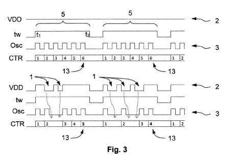
Fig. 3 schematically illustrates the basic concept used by the present
solution to detect at least one glitch 1 in an electrical signal 2. The upper
part
of Fig. 3 illustrates a first instance where no glitch is present in the
electric
signal 2. In contrast, the lower part of Fig. 3 corresponds to a second
instance
where several glitches are present in the electrical signal 2. In this Figure,
glitches are schematically represented by variations of square shapes
according to a digital glitch model.
Glitches 1 can occur at any time, in any manner and can therefore be
regarded as fully asynchronous in synchronous designs. From the
aforementioned electric signal 2, where glitches 1 may occur as shown in Fig.
CA 03065884 2019-12-02
WO 2018/229029
PCT/EP2018/065445
8
3, the present solution proposes to generate at least one digital oscillating
signal 3 which is sensitive to common glitches 1. To this end, at least one
digital oscillator, especially a ring oscillator, may be used as digital
generator
for generating the digital oscillating signal 3. The role of the digital
oscillator(s)
is to make possible the detection of any glitches, including those occurring
between the rising and falling edges of a clock signal 4 (Fig. 2).
Accordingly,
the solution proposes the use of asynchronous logic to detect glitches within
a
circuit designed for synchronous logic.
The basic concept is to use at least one free running digital oscillator to
determine, during a lapse of time, a sampling value characterizing this
digital
oscillator. From a theoretical point of view, if no glitch occurs the sampling
value will be always constant. In practice, some slight differences between
sampling values may occur, despite the absence of glitches. This may be
caused by jitter, e.g. variations in the period of the oscillator signal, and
other
variations within the circuit, e.g. temperature, voltage. However, if a single
glitch or a series of glitches occur, the sampling value will be clearly
different
from that provided by the digital oscillator when no glitch occurs.
To this end, the method of the present solution proposes to perform the
following steps as a repeatable round or cycle:
The first step of this round aims to assign a time window 5 to at least one
digital oscillating signal 3. This time window 5 is implemented on the basis
of
a clock signal 4 as shown in Fig. 2. This means that the time window 5 is
synchronous with the clock signal 4 and the duration of the time window is set
on a certain number of oscillations of the clock signal. The clock signal 4 is
substantially insensitive to the aforementioned at least one glitch 1 to
detect in
the electrical signal 2. This can be obtained through several embodiments, as
already discussed above in the summary of the present solution.
The second step of this round aims to determine, from the time window 5,
a sampling value 13 of the digital oscillating signal 3 to which this time
window
is assigned. This means that the sampling value 13 is determined from the
digital oscillating signal 3 to which the aforementioned time window 5 is
assigned and, more particularly, within the time limits ti-t2 defined by this
time
CA 03065884 2019-12-02
WO 2018/229029
PCT/EP2018/065445
9
window. The sampling value 13 is a value that characterizes the digital
oscillating signal 3 throughout its time window 5. Typically, such a value 13
may refer to the number of oscillations, pulses which may be positive and/or
negative pulses, periods or edges which may be raising and/or falling edges
of the digital oscillating signal 3 throughout its time window 5.
Alternatively,
the sampling value 13 may refer to value that derives from at least one of the
examples of values listed above. For instance, the sampling value may refer
to the frequency of the digital oscillating signal 3 during the time interval
ti-t2
defined by its time window 5.
As shown in the example depicted in Fig. 3, the sampling value 13
corresponds to the number of pulses provided by the digital oscillating signal
3
during its time window 5, i.e. between ti and t2. This number of pulses may be
determined by a counter CTR configured to count each pulse of the digital
oscillating signal 3 within the time window 5. Accordingly, the counter is
reset,
e.g. to zero, at the beginning of the time window: at instant ti, and then
counts
each pulse of the digital oscillating signal 3 until the end of the time
window: at
instant t2. As shown in the upper part of Fig. 3, the sampling value 13 is
constant and is equal to 6 due to the fact that the digital oscillating signal
3 is
also constant and especially not affected by glitches since no glitch is
present
in the monitored electrical signal 2.
The next step of the round aims to detect any potential glitch 1 in the
electric signal 2 which can be regarded as a monitored electric signal. Such a
step is performed by comparing the sampling value 13 with an expected
reference value 23. This reference value 23 may be for example a nominal
value provided by the digital oscillating signal 3 under normal conditions,
without any glitches 1. For example, the reference value 23 may be the
number of oscillations of the digital oscillating signal 3 within its time
window 5
under normal conditions, especially when no glitch 1 occurs on the electric
signal 2.
The last step of the round aims to output a response typifying a result of
the comparison made in the former step. The result of the comparison may
depend on the comparison itself, i.e. it may depend on the values compared
and the comparison operation which is used, such as >, <, =, 0, E, "--",
<<,
CA 03065884 2019-12-02
WO 2018/229029
PCT/EP2018/065445
>>. For example, if the sampling value 13 is equal to the expected reference
value 23, the response provided as output of this comparison may be a single
bit "1", otherwise a bit "0" may be output. A lot of other comparisons should
be
applicable without necessarily providing a binary response, i.e. a response
5 which is limited to two states. For example, the response may correspond to
"11" if the difference between the sampling value 13 and the reference value
23 is greater than five, otherwise the response may correspond to "01" if this
difference is greater than one, and finally if none of these cases is
satisfied,
then the response may correspond to "00".
10 Referring now to the lower part of Fig. 3, one can note that some
glitches
1 occur in the monitored electrical signal 2. Given that the digital
oscillating
signal 3 is generated from the electrical signal 2 and is sensitive to common
glitches i.e. glitches 1, this means that the digital oscillating signal 3 is
sensitive to the same glitches as those occurring in the electrical signal 2.
Due
to the glitch sensitivity of the digital oscillating signal 3, one can see
that the
latter is affected by the glitches occurring on the electrical signal 2.
Indeed, in
the upper part of Fig. 3, the sampling value 13 is always equal to six,
whereas
in the lower part it is firstly equal to five, then to four. Some pulses of
the
digital oscillating signal 3 were lost because this signal 3 has been
generated
from the electrical signal 2 and the latter has been affected by glitches 1.
Consequently, if the reference value 23 was set to six, the comparison
between the sampling value 13 and the reference value would indicate that no
glitch has been detected in the electrical signal of the upper part of Fig. 3,
whereas the same comparison would indicate the presence of at least one
glitch in the case of the lower part of Fig. 3.
Time window variants and/or digital oscillating signal variants
Fig. 4 schematically illustrates alternate embodiments, especially
regarding the time window 5. More specifically, this Figure shows three
different embodiments which may be used as variants within the solution
suggested in the present disclosure. Each embodiment is shown with a
horizontal time axis t. The time windows 5, 5' successively assigned to the
CA 03065884 2019-12-02
WO 2018/229029
PCT/EP2018/065445
11
digital oscillating signal through the repeated steps of the round may be
regarded as a so-called "time window signal" tw1.
According to the first embodiment, the time interval between two
successive time windows 5, 5' is as small as possible. Preferably, this time
interval will not excess the time required to:
- compare the sampling value 13 with the expected reference value 23, so
as to obtain a result, and
- assign a new time window 5' to the appropriate digital oscillating signal
3
in order to be ready to determine a new sampling value 13.
Once the result of the comparison is determined, the response typifying
the result of the comparison may be output either within the aforementioned
time interval, i.e. between two successive time windows, or subsequently, e.g.
during the next time window 5'.
The second embodiment disclosed through Fig. 4 is depicted in the
central part of this Figure through the so-called time window signals tw2a and
tw2b. Instead of using successive time windows 5, 5' provided by a single
time window signal tw1, the second embodiment suggests using two parallel
time windows signals tw2a, tw2b which are desynchronized with respect to
each other. More specifically, one can note in this second embodiment that
the time interval between two successive time windows 5a, 5b, 5'a, 5'b, along
the time axis t, is further minimized compared to that of the first embodiment
of Fig. 4. In the case shown in the median part of Fig. 4, this time interval
is
reduced to zero because the windows 5a and 5b, or 5'a and 5'b, are out of
phase, namely when the time window 5a or 5'a begins, the time window 5b,
respectively 5'b, ends. Thus, the falling edge of the time window 5a, or 5'a,
coincides with the rising edge of the time window 5b, respectively 5'b.
Accordingly, two successive time windows, e.g. 5a, 5b, or 5'a, 5'b are
temporally contiguous.
The third embodiment of Fig. 4 is shown at the bottom of this Figure
through two parallel time windows signals tw3a, tw3b. Instead of the time
windows 5a, 5b, 5'a, 5'b succeeding each other perfectly, by reducing the time
interval between two successive time windows to zero, there is an overlap
CA 03065884 2019-12-02
WO 2018/229029
PCT/EP2018/065445
12
between these time windows. Accordingly, the time interval between two
successive time windows may be regarded as being negative, in contrast with
that of the single time window signal tw1 where it may be regarded as being
positive. Such an overlap can be obtained using two identical time window
signals tw3a, tw3b, as shown in the bottom of Fig. 4, or it may be obtained by
using time windows 5a, 5b, or 5'a, 5'b, which are different. In any case, two
successive time windows, e.g. 5a, 5b, or 5'a, 5'b temporally overlap, whatever
the duration of the overlap.
Each of the time windows 5', 5'a, 5'b may be regarded as an additional
time window assigned on the relevant digital oscillating signal 3. Thanks to
the
time window 5 and to the at least one additional time window 5', 5'a, 5'b,
more
than one sampling value 13 may be determined to monitor the electric signal
2. Preferably, one sampling value 13 may be determined from each time
window 5, 5' or 5a, 5'a, 5b, 5'b. Still preferably, said at least one time
window
refers to time windows 5b, 5'b from each of which one sampling value 13 can
be determined in addition to the sampling value 13 determined from the time
window 5a, 5'a. In this way, several sampling values 13 can be
advantageously determined in parallel relative to one another, as shown in the
two last embodiments as shown in Fig. 4. In this way, the electric signal 4
may
be advantageously monitored in continuous way, i.e. without time interruption.
The implementation of any embodiment based on two so-called "time
window signals", may be obtained through two rounds of steps running in
parallel. A first round may be in charge of the implementation of the set of
the
first time windows 5a, 5'a, whereas the set of the second time windows 5b, 5'b
may be implemented by a second round running in parallel with the first
round. The two rounds may be synchronized each other so as to obtain the
second or the third embodiment of Fig. 4. Such synchronization may be
obtained thanks to the clock signal 4 which can be used for any signals or any
operation within a synchronous design or architecture.
A single digital oscillating signal 3 may be used for the two time windows
5a, 5b (5'a, 5'b) of the embodiments shown in Fig. 4. However, each time
window 5a, 5b (5'a, 5'b) may be applied to its own digital oscillating signal
3.
In this case, at least two digital oscillating signals 3 may be generated in
CA 03065884 2019-12-02
WO 2018/229029
PCT/EP2018/065445
13
parallel. These digital oscillating signals 3 may be identical or different
each
other. In other words, the frequency of a first digital oscillating signal
onto
which the first set of time windows 5a, 5'a is applied may be different from
the
frequency of a second digital oscillating signal onto which the second set of
time windows 5b, 5'b is applied.
It should be noted that even if there is a single so-called "time window
signal" twl , as shown in the upper part of Fig. 4, the time windows 5, 5' may
be applied onto more than one digital oscillating signal 3, either
simultaneously or alternatively. For instance, some time windows, e.g. odd-
numbered time windows if they were numbered, may be applied onto a first
digital oscillating signal 3, whereas the other time windows, e.g. even-
numbered time windows, may be applied onto a second digital oscillating
signal 3. There is no requirement for the first and second digital oscillating
signal to be identical. Alternatively, one can further consider having a
single
digital oscillating signal 3 whose frequency is modulated in accordance to the
number of the time window 5, 5'. For example, the digital oscillating signal 3
may have a first frequency fl for odd-numbered time windows 5, whereas the
same digital oscillating signal 3, i.e. a signal 3 generated by the same
generator, may have a second frequency f2 for even-numbered time windows
5'. Since the oscillating signal 3 is digital, therefore it may be obtained by
a
digital oscillation generator which can be set depending on the current time
window 5, 5', so as to generate digital oscillating signal sometimes having a
first frequency fl and sometimes a second frequency f2.
Whatever the embodiment, it should be noted that the maximum number
of digital oscillating signals 3 or frequencies of such a signal is no case
limited
to two.
Other embodiments
According to a preferred embodiment, the clock signal 4 is a third party
input signal or, in other words, a clock signal 4 which is provided, as input
signal, by a third party device. Since the only signal which may be analog in
the basic concept of the present solution is the clock signal 4, this
additional
CA 03065884 2019-12-02
WO 2018/229029
PCT/EP2018/065445
14
embodiment provides a solution in which no analog signal is generated, or a
solution where no analog data is generated.
Indeed, even if the clock signal 4 is an analog signal issued from an
analog clock generator, this clock signal 4 is merely used as input data, or
input signal, from a third party device or third party system which is
external to
the present solution. Accordingly, each step of the present solution may be
performed by a digital component or several digital components.
Advantageously, the solution provided in accordance to this embodiment
can be qualified as a full digital solution. It may provide significant
advantages
in terms of development, optimization, as miniaturization for example, and
achievement. For example, such a full digital solution may be easily
implemented under a software-based solution or a small form factor at a very
low cost for many technical applications, e.g. in fields such as banking,
telephony, computing, pay-TV and so on.
According to one embodiment, the clock signal may be generated from a
power supply signal, such as analog power supply signal, which is dissociated
from the electrical signal 2. This would mean that the signal used to power
the
oscillation generator from which the clock signal 4 is generated would be
decoupled from the monitored electric signal 2. Advantageously, such an
embodiment allows to ensure that the clock signal 4 will not be affected by
any glitch occurring on the electrical signal 2. If the power supply is of
high
quality, then glitches are more likely to be feared from hacker attacks. By
decoupling the clock signal 4 from the power supply signal, it becomes
possible to isolate the clock signal 4 from any glitch attack. Consequently,
if
the clock signal 4 can no longer be affected by glitches, then this clock
signal
4 may be generated by a digital oscillator, such as a ring oscillator, instead
of
being generated by an analog oscillator. This also means that in such a case,
the basic concept of the present solution may also be regarded as a full
digital
solution.
According to one embodiment, the time window 5, 5', 5a, 5'a, 5b, 5'b has
a duration which does not exceed one period of the clock signal 4.
Accordingly, the response time provided by the round can be optimized. The
CA 03065884 2019-12-02
WO 2018/229029
PCT/EP2018/065445
duration of the time window defines the time interval during which at least
one
glitch can be detected. However, the higher is this duration, the longer will
be
the response time since the result of the comparison of the sampling value 13
with the expected reference value 23 cannot be determined before the end of
5 the time window. Therefore, the duration of the time window may result
from a
compromise between the time range assigned to the glitch detection and the
response time of each round.
Furthermore, the frequency of the digital oscillating signal 3 has also an
impact on the sensibility of the glitch detection. Indeed, providing the
digital
10 oscillating signal 3 with a low frequency does not allow to have a
glitch
detection with a fine granularity. In contrast, if the digital oscillating
signal 3
has a high frequency, the granularity of the response provided by the round
will be much finer. On the other hand, a high frequency involves more
computing resources and more energy consumption than a low frequency.
15 The energy consumption may be regarded as a significant parameter,
especially for autonomous small form factor solutions such as those
embedded in smart cards for example.
In order to optimize the response time of the present solution, a first step
may intend to reduce as much as possible the time interval between two
successive rounds. To this end, the round may preferably be repeated as
soon as it is ended or completed, in order to optimize the glitch detection.
According to one embodiment, such an optimization may also be obtained
by adjusting the time window 5, 5', 5a, 5'a, 5b. 5'b, e.g. to specific
requirements. To this end, the time window may be configured using at least
one input parameter to set a specific duration. Setting the duration of the
time
window may be performed during an initial phase, for example before the
round(s) is/are triggered. Each time window 5, 5', preferably each set of
parallel time window 5a, 5'a and 5b, 5'b, may be configured using specific
input parameters or values. Alternatively, a single parameter or set of
parameters or values, may be applied to all time windows in order to set a
specific duration to these time windows.
CA 03065884 2019-12-02
WO 2018/229029
PCT/EP2018/065445
16
Similarly, the frequency of the digital oscillating signal 3 may also be set
or configured using an input parameter or at least one additional input
parameter. Advantageously, this embodiment allows to adjust the frequency
or frequencies, e.g. f1, f2, of any digital oscillating signal 3, in similar
way to
that performed to adjust the duration of the time window.
According to a preferred embodiment, the sampling value 13 refers to a
number of oscillations of the digital oscillating signal 3 throughout its
related
time window 5. The number of oscillations may be determined by a counting
function. To this end, a counter can be reset at the beginning of the time
window, and the counting can start at the rising edge of the time window and
can be stopped at the falling edge of the same time window. For this purpose,
a synchronization step may be added to trigger and stop the counting function
respectively at the rising edge and at the falling edge of the time window.
The
number of oscillations of the digital oscillating signal 3 can be counted,
throughout the time window, by several manners, for example by counting all
rising edges or falling edges of the digital oscillating signal 3. In a
variant,
pulses of the digital oscillating signal 3 may also be determined and counted,
e.g. by detecting each time this signal 3 reaches a predefined amplitude
level.
Although the sampling value 13 may also refer to the frequency of the
digital oscillating signal 3, it is more efficient to count, for example, all
the
rising edges of this signal 3, because a result is obtained more quickly than
if
the frequency has to be determined. Accordingly, the efficiency of the round
is
increased both in terms of speed and computing resources, while finally
improving the efficiency of the glitch detection.
According to another embodiment, the digital oscillating signal 3 may be
further filtered from any noise and/or jitter effect before determining the
sampling value 13. To this end a filtering function may be applied at the
output
of the generator providing the digital oscillating signal 3, so as to obtain a
filtered digital oscillating signal 3. Advantageously, such a filter or
filtering
function may be parameterized by input data, so as to adjust its filtering
level
e.g. at a predefined setting value. It should be noted that one can also
disable
the filtering function, e.g. by bypassing the filtering function or by setting
the
filtering level to one of its extreme levels. Such settings or adjustments may
CA 03065884 2019-12-02
WO 2018/229029
PCT/EP2018/065445
17
typically be performed during the initial phase mentioned above. Still
advantageously, by working with a digital oscillating signal 3 that is already
filtered, it is not necessary to add any filtering step in the round of the
present
solution. Therefore, the required time to execute the round is advantageously
shortened while improving its response time.
Glitch detection locations
To further increase the efficiency of the glitch detection, strategic
locations
may be taken in account as additional particular embodiments to apply the
steps of the present solution.
Glitches can be propagated inside a circuit through various paths which
cannot be known in advance. However, some techniques developed in the
laboratory have helped to identify specific locations that appear to be more
strategic than others.
From an input voltage applied to the power supply terminals, e.g. GND,
VDD, of a circuit, the voltage gradient through this circuit can be modeled in
the form of a grid in which each mesh or node corresponds to a certain
voltage. Therefore, such a grid may be regarded as a power supply grid which
reproduces the power distribution plan within the circuit. Due to the
resistance
of the interconnections and components constituting the circuit, there is a
voltage drop across the circuit commonly referred to as the IR-drop. The IR-
drop can be modeled e.g. through software simulations. A static IR-drop
analysis can be regarded as a representation of the power mesh quality
performed in accordance with statistical or specific power consumption which
typically depends on the number of gates, the frequency, the activity per
circuit block and so on. A dynamic IR-drop analysis can be obtained using
different functional scenarios.
Fig. 5 shows a flow chart of a process which may be used to determine
the best locations, i.e. physical positions, where it should be suitable to
perform glitch detections within a circuit. Indeed, the glitch detection
according
to the present solution is not limited to the detection of glitches on power
supply, but it may be used for detecting glitches on any electrical signal 2
within a circuit.
CA 03065884 2019-12-02
WO 2018/229029
PCT/EP2018/065445
18
Box 20 illustrates the beginning of the process which may be
implemented, for example by using a computer-implemented algorithm.
Two main parallel paths appear just after the beginning. One of these
path, in this case the left one, refers to steps performed in accordance with
a
static analysis, whereas the other path, i.e. the one on the right, refers to
steps performed in accordance with a dynamic analysis.
At boxes 22a and 22b, respectively static and dynamic power constraints
are applied to the circuit.
At boxes 24a and 24b, a static IR-drop analysis, respectively a dynamic
IR-drop analysis is launched.
At box 26a, a weak static spot and a strong static spot are identified. In
the same way, at box 26b, a weak dynamic spot and a strong dynamic spot
are identified.
The two aforementioned paths meet at box 28 in order to check if there
are common weak and strong spots. In other words, the operation undertaken
at box 28 aims to look for common weak static-dynamic IR-drop and also aims
to look for common strong static-dynamic IR-drop in order to increase the
chance to get the most pertinent spot to observe.
At the next box 30, the present solution for detecting at least one glitch is
applied at strategic locations identified at steps 26a, 26b. Preferably these
strategic locations are refined, e.g. still at boxes 26a, 26b, so as to
identify a
spot where a potential difference with respect to one power supply terminal
e.g. GND or VDD, of the circuit is high or low, still preferably the highest
or the
lowest. Still preferably, the strategic locations are those identified at box
28.
Whatever the embodiment, it should be understood that at least one of
these strategic locations may be used to perform glitch detection.
Accordingly, the steps of the solution suggested through the basic
concept or any of its embodiments are applied on the electrical signal 2 of a
circuit, preferably at those strategic locations, for example physical
positions,
or at least one of those strategic locations. Providing glitch detection at
strong
CA 03065884 2019-12-02
WO 2018/229029
PCT/EP2018/065445
19
IR-drop places, i.e. locations, and at weak IR-drop places, i.e. locations,
allows to cover the most sensitive locations across the circuit or the chip.
Alternatively, the aforementioned electric signal can refer to that of a
specific block or portion of the circuit, instead of referring to the entire
circuit
which may comprises several separate blocks or distinct portions.
Accordingly, specific parts of a circuit such as sensitive blocks may be
protected against glitches. Particular strategic locations may be reached,
especially thanks to the miniaturization provided by the so-called "full
digital"
present solution. Indeed, the present solution gives access to new locations
that remain impossible to reach using conventional solutions based one or
more analog components.
Regarding the last box 32, it may be regarded as the end of the process
or algorithm.
A third path, parallel to the aforementioned two main parallel paths, may
also be taken from the beginning for checking locations of block to protect,
as
schematically shown through box 22c. Once this operation is achieved, the
process through this third path may directly join the box 30. The third path
schematically depicts some iterations that may be executed in order to obtain
some refinements of the process.
The basic concept of the solution disclosed so far, or any of its
embodiments, may be applied through a method suitable to detect at least
one glitch in an electrical signal. Such a solution, including any of its
embodiments, may also be applied by a device or a system. Accordingly, the
next part of the present disclosure will especially refer to a device for
implementing the aforementioned method, including any of its embodiments.
Device for implementing the method of the present solution
Fig. 6 provides an example of a main architecture of a device 40 for
implementing the method based on any embodiments disclosed so far. As
shown, the device 40 may comprises:
CA 03065884 2019-12-02
WO 2018/229029
PCT/EP2018/065445
at least one digital oscillator 43 in order to generate the at least one
digital
oscillating signal 3;
a data interface 45 configured to output or exchange data beyond the
device 40; and
5 a
computing unit 50 configured to perform at least the steps of the
repeatable round or cycle disclosed above.
The device 40 is provided with power supply terminals 41, e.g. GND and
VDD. Preferably, the clock signal 4 CLK is input into the device 40 as input
signal. Such an input signal may be generated by a third party device or
10 entity,
typically by a clock generator which is external to the device 40 and
which may generate the clock signal as a reference signal for an entire
system whose the device 40 could be just one part of such a system.
Advantageously, by receiving a clock signal 4 from a third party entity
external to the device 40, this device 40 can be regarded as a so-called "full
15 digital"
device. It may be made from a CMOS standard cells library and is fully
synthesizable. Accordingly, the functions provided by the device 40 may be
fully simulated, for example using a simulation program such as SPICE
(Simulation Program with Integrated Circuit Emphasis). In other words, the
operating steps of such a device 40 may be also recorded in the form of
20 program
steps, within a text file, to be executed by a microprocessor.
Therefore, the present solution may be easily used through IP technology.
Still advantageously, it has no particular backend requirements and no
extra hard macro development impact. The device 40 has very compact sizes
and can take advantage of all the other benefits already mentioned above in
connection with the former part of the present disclosure. Nevertheless, the
clock signal 4 may be also generated by a dedicated clock generator located
within the device 40, as already explained.
As shown in Fig. 6, the device may receive other signal as input signal,
such as a reset signal 44. Such a reset signal 44 may be used to reset some
data or parameter of the device 40, for example to totally or partially
restore
the factory configuration of the device 40. The reset signal 44 may be
CA 03065884 2019-12-02
WO 2018/229029
PCT/EP2018/065445
21
triggered for example by pressing a reset button from the external side of
device or by receiving a remote command having the same effect.
Preferably, the digital oscillator 43 is a ring oscillator which may be made
according to any one of the embodiments well known by the person skilled in
the art. As a reminder, a ring oscillator is a device at least composed of odd
number of inverter, i.e. NOT gates, in a ring, whose output therefore
oscillates
between two voltage levels. The inverters are attached in a chain and the
output of the last inverter is fed back into the first inverter of the chain
so as to
create a loop or a ring. Delay cells or buffers may be added to increase the
temporal offset of the signal between the two ends of the chain of inverters.
A
specific and preferred embodiment of a ring oscillator is shown in Fig. 6 and
will be described in more detail later.
The data interface 45 of the device 40 is mainly configured to send or
exchange any kind of useful data between the device 40 and its external
environment. Preferably, the data interface 45 is connected to the computing
unit 50 within the device 40. On the other side, i.e. at the external of the
device 40, the data interface 45 may be connected to any kind of external
units 60, for example to a micro-controller 61, a direct memory access 62 to
store data or any other kind of memory 63.
Regarding the computing unit 50, this unit may be configured to perform
any operation in connection with at least one of the digital oscillator 43,
data
transmitted through the data interface 45 and the signals 4, 44, 41 received
as
input signal in the device 40. Furthermore, the computing unit 50 may
comprise a setting unit 52, a synchronizing unit 54, and a filtering unit 56.
Instead of being located in the computing unit 50, any of these units 52, 54,
56 may be located outside the computing unit 50, while remaining inside the
device 40. The same may be true for other units not shown in Fig. 6, such as
a counting unit for counting the sampling value 13, a comparing unit for
comparing the sampling value 13 with the expected reference value 23 or a
memory unit for storing any kind of values or parameters such as the
reference value 23. These units have not been shown in Fig. 6 because their
functions may be performed by the computing unit 50 without requiring
specific units. The same should be applicable with the functions provided by
CA 03065884 2019-12-02
WO 2018/229029
PCT/EP2018/065445
22
the units 52, 54 and 56 which, for this reason, have been each drawn using a
broken line within the computing unit 50.
The setting unit 52 may be used to set some parameters or values used in
any function, algorithm or steps within the device 40. Such a setting unit 52
may typically operable with the data interface 45 for receiving or exchanging
data to be used for setting purposes. As already explained in connection with
the first part of the present disclosure, data, values or parameters may be
used e.g. to set any time window or duration, the frequency of the digital
oscillating signal 3 to be output from the digital oscillator 43 or the
filtering
levels of a filtering function to be applied at the output of the digital
oscillating
signal 3, for instance.
The synchronizing unit 54 may be used for several purposes. For
example, it can be used to implement the synchronization step designed to
trigger and stop the counting function respectively at the rising edge and at
the falling edge of the time window. The synchronizing unit 54 may also be
used to synchronize the time windows with each other or to synchronize the
rounds with each other if several rounds are running in parallel.
The filtering unit 56 may be especially used to filter the digital oscillating
signal 3 from any noise or jitter. Accordingly, a clear digital oscillating
signal 3
can be obtained and used by the computing unit 50 to identify any glitch,
without any ambiguity.
Although a single digital oscillator 43 has been shown in the device 40 of
Fig. 6, it should be noted that this device 40 may comprise more than one
digital oscillator 43, depending on the number of digital oscillating signals
3
that are needed to implement any embodiment already discussed above.
The device 40 may be manufactured as a monolithic device, for example
in a single chipset.
Fig. 7 shows the architecture of a ring oscillator used in the present
solution as preferred digital ring oscillator 43. As shown in this Fig.7, this
ring
oscillator is based on a three states ring selection, where the inputs E0, El
and E2 are used to enable and to select the ring loop frequency of the ring
CA 03065884 2019-12-02
WO 2018/229029
PCT/EP2018/065445
23
oscillator 43 thanks to three possible loops. The input E0 is the input which
activates the main ring loop.
This ring oscillator 43 always comprises an odd number of inverters 43a,
as a NOT gates, in the ring path. In this case a single inverter 43a, such as
single NOT gate, is used as example. This ring oscillator further comprises
other logic gates 43b, as a AND gates. In addition, it comprises delay cells
43c which are especially used to increase the temporal offset of the signal
between the inputs and the outputs of the loop of the ring oscillator 43.
Finally,
it comprises tri-states 43d.
Advantageously, the use of logic gates allows to reduce the power
consumption. Indeed, in the present ring oscillator 43, the number of gates,
in
combination with an adequate clock gating, allows to cut the power
consumption in the non-active part of the ring.
Thanks to such a ring oscillator 43, multiple frequencies may be selected
so as to respond to different process variations and conditions of use of the
circuit while remaining suitable to detect a whole range of glitches.
Accordingly, the frequency may be selected so as to detect glitches whose
detection may be affected by the specification dispersion of certain
components of the circuit. By increasing the frequency of the digital
oscillator,
.. it becomes possible to improve the glitch detection so as to cover the
entire
range of such a dispersion.
The device 40 may be used in many technical fields. For example, it may
be especially convenient for implementing the method of the present solution
in the next smart cards generation. Thanks to the present solution, it becomes
possible to detect any glitch occurring on the internal power supply of a
device
or system by using digital circuitry as logic circuits.
It should be noted that any other feature mentioned in connection with the
method remains valid for the present device 40. However, for the sake of
conciseness, the present disclosure refrains from repeating all variants and
.. embodiment which may also be applied to the device 40.
CA 03065884 2019-12-02
WO 2018/229029
PCT/EP2018/065445
24
Final considerations
Although an overview of the inventive subject matter has been described
with reference to specific example embodiments, various modifications and
changes may be made to these embodiments without departing from the
broader spirit and scope of embodiments of the present invention. For
example, various embodiments or features thereof may be mixed and
matched or made optional by a person of ordinary skill in the art. The
Detailed Description, therefore, is not to be taken in a limiting sense, and
the
scope of various embodiments is defined only by the appended claims, along
with the full range of equivalents to which such claims are entitled.