Note: Descriptions are shown in the official language in which they were submitted.
CA 03067098 2019-12-11
WO 2019/010028
PCT/US2018/039294
SECONDARY CIRCUIT AND TIMING DEVICE FOR APPLIANCE
Cross-Reference to Related Applications
[0001] This application claims priority to and the benefit of U.S. Patent
Application No.
15/643,541, filed July 7, 2017, the entire contents of which is incorporated
herein by
reference in its entirety.
Background
[0002] The present invention is directed to a power cut-off circuit
configuration, and in
particular to a secondary power cut-off device for an appliance, such as a
toaster.
[0003] Appliances, such as toasters, can utilize heating elements or other
components to heat,
toast, and/or cook items, such as food to be toasted. Heating elements
generally convert
electricity into heat by passing the electricity through a metal of high
resistivity, causing
energy passing therethrough to be converted to heat that is emitted by the
heat element. Some
examples of heat element materials include Nichrome (nickel and chromium),
ceramic
materials (such as molybdenum disilicide), polymers, composites, and
combinations thereof.
During appliance use, one or more heating elements may cause items being
heated thereby to
become overheated in cases of overuse or malfunction. For example, it can be
undesirable to
heat a food item too long.
[0004] To date, various mechanical and circuit-based configurations have been
used to limit
the heating and control timing related to appliance misuse or malfunction. For
instance, in
one example, a thermal sensor is built into an appliance, which can signal to
a heating control
unit that the item being heated is at risk of being overheated based on a heat
and time-based
threshold.
Summary
[0005] The present invention overcomes shortcomings of the prior art by
introducing a
secondary circuit configured to automatically break an appliance heating
element power
circuit after a set time that is preferably chosen to be longer than the
maximum time an item
can be cooked by the appliance heating element.
1
CA 03067098 2019-12-11
WO 2019/010028
PCT/US2018/039294
[0006] According to a first aspect, a circuit configuration is disclosed for
use in an appliance.
The circuit configuration includes a power switch electrically coupled to a
power source, the
power switch configured to open and close a first group of electrical
contacts, where the
contacts while closed cause the appliance to energize upon a user initiating a
use of the
appliance. The circuit configuration also includes a primary timing device
electrically
connected to the first group of electrical contacts, the primary timing device
being actuated
upon energization of the appliance and the primary timing device being
configured to de-
energize the appliance after a first time period by opening the first group of
electrical
contacts. The circuit configuration also includes a secondary timing device
electrically
connected to the power switch by a second group of electrical contacts, where
the secondary
timing device is configured to de-energize the appliance after a second time
period, where the
second time period is set based on the first time period, and where the second
time period is a
third time period longer than the first time period.
[0007] According to a second aspect, toaster including a power cut-off
function is disclosed.
The toaster includes a power switch electrically coupled to a power source,
the power switch
configured to open and close a first group of electrical contacts, where the
contacts while
closed cause the appliance to energize upon a user initiating a use of the
appliance. The
toaster also includes a primary timing device electrically connected to the
first group of
electrical contacts, the primary timing device being actuated upon
energization of the
appliance and the primary timing device being configured to de-energize the
toaster after a
first time period by opening the first group of electrical contacts. The
toaster also includes a
secondary timing device electrically connected to the power switch by a second
group of
electrical contacts, where the secondary timing device is configured to de-
energize the
appliance after a second time period, where the second time period is based on
the first time
period, and where the second time period is a third time period longer than
the first time
period.
[0008] According to a third aspect, a method for controlling an appliance is
disclosed. The
method includes receiving an input to energize an appliance, where the
appliance includes a
heating unit. The method also includes activating a primary timing device of
the appliance
upon the energizing the appliance, where the primary timing device is
connected to a first
group of electrical contacts, and where the primary timing device is
configured to de-energize
the appliance after a first time period by opening the first group of
electrical contacts. The
2
CA 03067098 2019-12-11
WO 2019/010028
PCT/US2018/039294
method also includes setting a second time period based on the first time
period, where the
second time period is set to be a third time period longer than the first time
period. The
method also includes activating a secondary timing device of the appliance
upon the
energizing the appliance, where the secondary timing device is connected to a
second group
of electrical contacts, and where the secondary timing device is configured to
de-energize the
appliance after the second time period.
Brief Description of the Drawings
[0009] FIG. 1 is a schematic representation of a toaster system including a
toaster, according
to various embodiments.
[0010] FIG. 2A is an example configuration of an appliance power supply
circuit, according
to various embodiments.
[0011] FIG. 2B is a controller circuit for use with power supply circuit in an
appliance,
according to various embodiments.
[0012] FIG. 3 is an embodiment of a transistor-based secondary circuit,
according to an
aspect of the present invention.
[0013] FIG. 4 is a transistor and integrated-circuit-based embodiment of a
secondary circuit,
according to an aspect of the present invention.
[0014] FIG. 5 is another embodiment of a transistor-based secondary circuit,
according to an
aspect of the present invention.
[0015] FIG. 6 is a graph showing a first time period t, a second time period
t+n, and a third
time period n, according to various embodiments.
Detailed Description of the Preferred Embodiments
[0016] FIG. 1 is a schematic representation of a toaster system 10 including a
toaster 16,
according to various embodiments.
[0017] Toaster 16 can be an appliance, as used herein. Toaster 16 can receive
an input 12, for
example, from a user, computer, or other external source. Input 12 can be
received at toaster
16 through various input methods and systems 14, such as buttons, knobs,
plungers, levers,
3
CA 03067098 2019-12-11
WO 2019/010028
PCT/US2018/039294
etc. Toaster 16 can include a carriage module 18, which can include a ferrous
element 20 and
an electromagnet 22, which can be used to hold down carriage 18. Electromagnet
22 can be
similar to electromagnet 136 of FIG. 2A, described below, according to various
embodiments.
[0018] Toaster 16 can also include a primary timing device 28, a secondary
timing device 32,
heating element(s) 30, a controller 26, and a power switch 24. Power switch 24
can be used to
regulate power flow from power source 34 to toaster 16, and may be actuated by
controller
26 and/or through primary timing device 28 or secondary timing device 32.
Additional
features and variations on the toaster 16 configuration are contemplated
within the scope of
this disclosure.
[0019] FIG. 2A is an example configuration of an appliance power supply (PS)
circuit 100,
according to various embodiments. According to the shown example, the circuit
can be
configured for use in an appliance, such as a pop-up electric toaster (an
example of which is
schematically shown as toaster 16 of FIG. 1).
[0020] PS circuit 100 can be separated into two circuit sub-components, with a
heating
portion 102 shown at left and an electromagnetic ejection portion 104 shown at
right of FIG.
2A. Alternatively, heating portion 102 and ejection portion 104 can compose a
single PS
circuit 100. Various electrical connection points are represented. A power
source 108 can be
an alternating current (AC) source, and may be preferably received at either
110-120V or
220-240V, 50-60Hz, and preferably at a power level of 1100-1300W, according to
various
embodiments. A main power switch 110 (e.g., power switch 24 of FIG. 1) can be
activated by
a user, computer system, or other control according to various embodiments.
Where the
example appliance is a toaster, pressing down on a carriage lever (e.g., part
of carriage
module 18 of FIG. 1) may activate power toaster power switch 110.
[0021] Power switch 110 may have a first group of electrical contacts
including a first pole
and a second pole, where the power switch 110 is connected at the first pole
to a line 112, and
at the second pole to a ground, an inner heater 113 and two outer heaters 111
and 115
connected in series, and a heater relay connection 114. Also connected to the
second pole is a
PS connection 120, and optionally two resistors shown in box 118, preferably
to be utilized
where a normally-open relay is employed in circuit 100 in the heating portion
102.
4
CA 03067098 2019-12-11
WO 2019/010028
PCT/US2018/039294
Electrically coupled to the resistors in box 118 are line connection 124 and
PS connection
126.
[0022] The other, ejection portion 104 of PS circuit 100 can preferably
include a PS
connection 116 with diodes, resistors, capacitors, transistor 134, and at
least one
electromagnet 136 (e.g., for use in carriage ejection), as shown. A 5V
connection 128 and
12V connection 117 may be included, along with a reheat connection 130, a
defrost
connection 132, and a control connection 122. Control connection 122, reheat
connection
130, and defrost connection 132 can be connected to a controller 200, as
described in FIG.
2B.
[0023] Various circuit components of PS circuit 100 (and other circuits,
herein) can be
selected such that various specifications of the circuit components is
appropriate based on
implementation and configuration. Such components could be selected for
various
configurations by those skilled in the art.
[0024] FIG. 2B is a controller circuit 200 for use with power supply (PS)
circuit 100 in an
appliance, according to various embodiments.
[0025] Controller circuit 200 is a primary controller circuit for an
appliance, preferably a
toaster (e.g., toaster 16 FIG. 1). Controller circuit 200 includes an
integrated circuit (IC) (e.g.,
an application-specific integrated circuit (ASIC)) 210, and connections for
the controller
circuit 200 to be operatively connected to PS circuit 100 of FIG. 2A. ASIC 210
can have
many connections, and can include many IC components, depending on
configuration.
Examples of ASIC 210 may include ICs, such as commercially-available CMS12560
and/or
A0201H timing chips, according to various embodiments. A 5V connection 218 to
ASIC 210
can be included, as shown. A reheat connection 212 may be configured to
connect to reheat
connection 130 of FIG. 1A, a defrost connection 214 may be configured to
connect to defrost
connection 132 of FIG. 1A, and control connection 216 may be configured to
transmit control
commands to control connection 122 of circuit 100 of FIG. 1A. Together,
circuits 100 and
200 may form a single circuit including both PS and control aspects of an
appliance,
according to various embodiments.
[0026] FIGs. 3-5 are three embodiments of a secondary circuit, according to
various
embodiments of this disclosure.
CA 03067098 2019-12-11
WO 2019/010028
PCT/US2018/039294
[0027] FIG. 3 is an embodiment of a transistor-based secondary circuit 300,
according to an
aspect of the present invention.
[0028] An appliance (e.g., toaster 16 of FIG. 1) can include (PS and control)
circuits 100 and
200 of FIGs. 2A and 2B, and can operate nominally under standard conditions
without further
safeguards against overheating. A secondary circuit 300, having an RC circuit
302 and a relay
circuit 304, can be introduced in order to prevent overheating of the toaster
and/or food item.
It is known that toasters employ a timing device to prescribe how long a piece
of bread,
bagel, etc. should preferably be toasted before ejecting. According to this
disclosure, a
secondary circuit 300 can be or include a secondary timing device (e.g.,
circuit 300) in order
to act as a power-cutting, circuit-breaking fail safe in a case where a
primary timing device
fails to operate properly.
[0029] When a user operates a toaster including the secondary circuit 300,
power switch 110
is closed (e.g., when a toaster carriage having a ferrous element is pressed
down) power is
applied to the circuit 300, a carriage-holding electromagnet (e.g., 136 of
FIG. 2A) is
energized and holds the carriage in place, using the ferrous element, against
biased ejection
springs (not shown). Circuit 300 can include a 12V electrical input 315 at the
RC circuit 302
and a 12V electrical input 317 at the relay circuit 304. Both 12V inputs can
be connected to
and received from PS connection 117, which can be a rectified, tapped a heater
winding, filter
it and then use it as a 12 volt supply. The carriage can be held down for a
set amount of time
based on either consumer settings or inputs of external toaster controls at a
primary timing
device (not shown). In some embodiments, the amount of time can be set by the
primary
timing device automatically based on conditions or detected requirements. Of
note, the
secondary circuit 300 (and secondary timing device) can have a time set based
on a time set
on the primary timing device. For example, a time set on the secondary circuit
can be 30
seconds longer than a time period set on the primary timing device. According
to various
embodiments, there may be a maximum time period setting for the primary timing
device.
According to another embodiment, a time period setting of the secondary
circuit 300 can be
set such that it is a time period longer than the longest possible setting of
the primary timing
device. The delay can be shorter or longer as determined to provide a desired
release using
relay circuit 304.
6
CA 03067098 2019-12-11
WO 2019/010028
PCT/US2018/039294
[0030] At the same time at the carriage is held down and the toaster begins
heating operation,
a direct current (DC) voltage (e.g., 12V from PS connection 117) can be
applied to a
secondary circuit 300 (or circuit 400 of FIG. 4, among other embodiments). As
shown,
transistor Q? 326 can preferably be selected to be a PNP transistor that can
operate as
normally closed (electrically connected) switches when no bias is applied to
the transistor
base. Transistor Q9326 can include a base, an emitter, and a collector. The
collector of
transistor Q? 326 can be electrically grounded, the base can be connected to a
resistor-
capacitor (RC) circuit 302, and the emitter can be connected to relay circuit
304. In this case,
no bias would be applied at toaster activation due to the RC circuit 302
composed of R2 at
316 and capacitor Ci at 320. The RC circuit 302 can be grounded, as shown.
[0031] As the RC circuit 302 charges up over time from a biased voltage input
(preferably
12V, as shown) from a PS connection 117, e.g., from PS 100 of FIG. 2A, the
transistor Q?
326 base becomes increasingly biased (shown also as charge curve 512 of FIG.
5), and
transistor Q? 326 having its base connected to the RC circuit 302 and emitter
connected to
relay circuit 304, can be reached through resistor R4 322. RC circuit 203 may
have a
characteristic charge time "tau," based on various components' specifications.
A reverse-bias
Zener diode 318 can be included in RC circuit 302, electrically connected on
an output end to
resistor R4 322 and capacitor C9324 (leading to transistor Q? 326 and a relay
334 and
associated relay switch 332 of relay circuit 304). The Zener diode 318 can be
connected on
the other end to resistors R2 316 and R3 314 and to capacitor Ci 320 within RC
circuit 302.
The Zener diode 318 (with a particular corresponding Zener breakdown voltage)
can be
placed in the base leg of transistor Q? 326 so that the circuit 300 and
transistor Q? 326 do not
activate until the specific Zener breakdown voltage has been reached during
the RC charge
time of RC circuit 302. The characteristic RC charge time may be a function of
the various
components of RC circuit 302. If the characteristic Zener breakdown is
reached, the relay
circuit 304 can de-energize a heating element (e.g., 30 of FIG. 1) of an
appliance (e.g., toaster
16 of FIG. 1). According to a preferred embodiment, relay 334 can be normally
open.
[0032] The closed switch 110 condition (see FIG. 2A), once adequate charge is
built up in
the RC circuit 302, applies voltage to the base of transistor Q? 326, thereby
turning transistor
Q? 326 "on." By turning on transistor Q? 326, relay 334 of relay circuit 304
is energized by
12V electrical input 317 from PS 100 connection 117. Relay 334 can be
connected in series
with the power switch 110. Also as shown, diode DI 328 (e.g., a commercially-
available
7
CA 03067098 2019-12-11
WO 2019/010028
PCT/US2018/039294
standard silicon switching diode, such as a 1N4148 signal diode) is of reverse-
bias and is
located in a circuit from transistor Q? 326 to ground in order to protect
transistor Q9326 from
back electromotive force (EMF) from the relay switch 332 of relay 334. Relay
switch 332 is
connected to relay 334, which is shown connected to line connection 330 and
heater relay
connection 336 at two electrical contacts or poles. Line connection 330 and
heater relay
connection 336 can then be used to de-energize the appliance, as described
herein.
[0033] Once the RC circuit 302 has been sufficiently charged after a time by
5V input 315,
RC circuit 302 can place a bias on the base of transistor Q9326 which opens
the closed switch
characteristic of transistor Q? 326, energizing relay 334. As relay 334 is
energized, the 12V
input from the relay 334 is removed at relay switch 332, thereby shutting down
and de-
energizing the heating element(s) of the appliance. The RC time constant
(e.g., tau) can be
chosen to be less than 30 seconds longer than the longest time period of the
longest toaster
setting, about 30 seconds longer, or more than 30 seconds longer.
[0034] Secondary circuit 300 can trigger after the RC time constant is
reached, and secondary
circuit 300 can remove (de-energize) all AC input power from the various
circuit components
by opening the power switch 110, and bias can be removed from transistor Q1312
through
resistor R1310, causing transistor Qi 312 to now operate as a closed switch,
allowing
capacitor C1320 to discharge through resistor R3 314 and thereby removing the
bias from
transistor Q? 326, and activating (or deactivating) relay circuit 304
accordingly.
[0035] FIG. 4 is a transistor and integrated-circuit-based embodiment of a
secondary circuit
400, according to an aspect of the present invention.
[0036] When the power switch 110 is closed (e.g., when the carriage of a
toaster is lowered
or pressed down) power is applied to a circuit 400, and the holding
electromagnet (e.g., 136
of FIG. 2A or 22 of FIG. 1) is thereby energized. The energized electromagnet
can hold the
carriage (e.g., carriage module of FIG. 1) in place for a set amount of time,
for example based
on consumer settings of the external controls. As explained with respect to
FIG. 3, a
secondary circuit 300 (e.g., a secondary timing device) can include an RC
circuit 302
including at least one resistor and at least one capacitor can be configured
to set the trigger
timing of the circuit. Alternatively, instead of employing an RC circuit 302,
the secondary
timing device and circuit can include a timer circuit 404 including a timer
circuit device, e.g.,
8
CA 03067098 2019-12-11
WO 2019/010028
PCT/US2018/039294
a "555," "556," "558," or "559" timer integrated circuit, as are commercially
available.
Examples of timer integrated circuits can include a plurality of transistors,
diodes, and
resistors on a silicon chip, and can include a plurality of connections, such
as grounds,
triggers, output, input, control, reset, etc. Based on inputs and
configurations, timer circuit
404 can be set for various time periods, including about 30 seconds longer
than the longest
time period of the longest toaster time setting, less than 30 seconds longer,
greater than 30
seconds longer, or any other suitable time longer than the applicable toaster
time setting.
[00371 As shown in FIG. 4, components including transistor Q? at 410, diode D?
at 414, relay
at 420, associated relay switch at 416, and line connection at 412 and heate
connection at 418
can be similar to the various connections described as to circuit 304 in FIG.
3. However,
instead of employing the RC circuit 302 of FIG. 3, FIG. 4, as shown, employs
the timer
circuit 404 including an integrated timing circuit device 428 configured to
set a time period
leading to increased appliance control. Also shown are capacitors C? 424, C2
432, C3 430,
resistor R5 426, and resistor trigger 422 connected to a positive 12V PS
voltage (e.g., VCC)
415, for example from 12V connection 117 ofPS circuit 100 of FIG. 2A. A second
PS VCC
419 can also be connected to resistor R5 426 and timing circuit device 428, as
shown. As
shown the integrated circuit can be in communication with various relays,
circuits, and
integrated circuit components, both shown and not shown in various
embodiments, herein.
Fewer overall components may be employed in circuit 400 than circuit 300,
according to
various embodiments.
[0038] As above, the timing circuit, when a time expires at timer circuit 404,
a relay signal is
sent via first relay connection 417 to second relay connection 411. When
second relay
connection receives a timer signal from first relay connection 417, transistor
Q9 410 activates
and allows VCC 413 to energize relay 420, triggering the relay 420 and an
associated relay
switch 416.
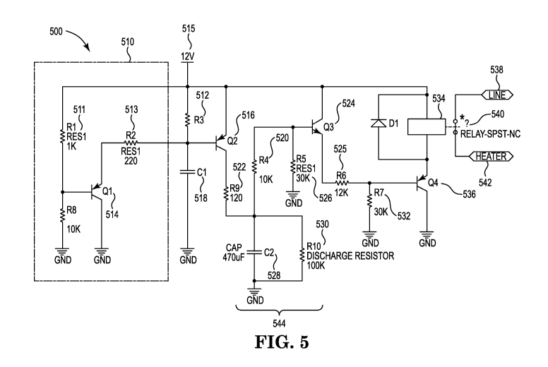
[00391 FIG. 5 is another embodiment of a transistor-based secondary circuit
500, according
to an aspect of the present invention.
[0040] Circuit 500 is another alternative, transistor-based embodiment of a
secondary circuit,
according to the present invention. Circuit 500 can include various
components, as shown,
and can be connected to a voltage source at 515 as well as a heating element
via line
9
CA 03067098 2019-12-11
WO 2019/010028
PCT/US2018/039294
connection 538 and heater connection 542. Circuit 500 can be similar to
circuit 300 of FIG. 3,
but, as shown, can include additional transistors and other circuitry. Circuit
500 can include a
transistor Q2516 having a base, a collector, and an emitter, an RC circuit
544, and
components 510 that can be configured to discharge a capacitor C1 518 in a
case where power
has been removed. Components 510 of circuit 500 can include a transistor Qi
514, which can
be a PNP-type transistor. Transistor Qi 514 can have a base, a collector, and
an emitter, with
the collector connected to base of transistor Q2516. Transistor Qi 514 can act
as a closed
switch connecting capacitor C1 to ground through resistors R2 513 and/or R3
512. Resistor R3
512 can act as a current-limit resistor protecting transistor Qi 514 from high
(e.g., short
circuit) currents possible during a discharge, for example of capacitor C1
518.
[0041] Transistor Q3 524 can have a base, a collector, and an emitter, as
shown. Transistor Q4
536 can be a relay coil, and can have a base, a collector, and an emitter,
with the collector
connected to a relay 534 having a relay switch 540. As shown, resistors R1 511
and R2 513
form a voltage divider which can be configured to keep a bias on transistor Q1
514. As long
as AC power is applied at 12V connection 515, the bias on transistor Qi 514
keeps transistor
Qi 514 from conducting. Transistor Q1 514 may be configured to conduct only
when AC
power has been removed. Then transistor Qi 514 can discharge capacitor C1 518.
[0042] Resistor R3 513 and capacitor C1 518, as shown, form an RC circuit
configured to bias
transistor Q2 516 after a period of time. The period of time should preferably
be long enough
to charge capacitor C2 528 through resistor R9 522. Once capacitor C1 518 is
charged, it can
place a bias on transistor Q2 516, which can cause transistor Q2 516 to stop
conducting,
thereby disconnecting a input voltage from resistor R9522 and capacitor C2528.
As shown,
capacitor C2 528 and resistor R10 530 can form an RC circuit 544 that is
configured to set the
timing for discharging the capacitor C2 528. In some embodiments, once
capacitor C1 518 is
charged and has therefore preferably placed a bias on transistor Q2 516,
capacitor C2 528 now
can become a power source for circuit 500 until capacitor C2 528 is drained of
its energy
charge.
[0043] Resistor R4 520 can be a base bias resistor for transistor Q3 524, and
resistor R5 526
can hold the base of transistor Q3524 low when no bias is applied, according
to various
embodiments. In various embodiments, transistor Q3 524 can drive the base of
relay coil
transistor Q4 536 through a resistor R6 525, keeping relay coil transistor Q4
536 from
CA 03067098 2019-12-11
WO 2019/010028
PCT/US2018/039294
conducting keeping the relay switch 540 de-energized which can keep relay 534
closed,
thereby allowing energy to the heaters via line connection 538 and/or heater
connection 542.
In a case where capacitor C2 528 has discharged and therefore removed the bias
from
transistor Q 524, transistor Q 524 may no longer place a bias on the base of
relay coil
transistor Q 536, causing relay coil transistor Q4 536 to begin to conduct,
thereby energizing
the relay coil transistor Q 536, and opening relay switch 540 via relay 534,
which is
configured to de-energizes one or more heaters via line connection 538 and/or
heater
connection 542. Once AC power has been disconnected (preferably through a
switch, such as
switch 110), then capacitor C1 518 can discharge and the process can restart
once AC power
has been restored to the circuit 500.
[0044] Stated different, at an initial appliance (e.g., toaster 16) startup
(e.g., when a carriage
is initially pressed down by a user), the base of transistor Q2516 can be held
low by resistor
R3512 and capacitor C1518. For example, capacitor C1 518 initial voltage
condition can
preferably be OV. This setup can preferably allow voltage to pass through
transistor Q2 516 to
charge capacitor C2528. As shown, resistor R9 522 can be a current-limiting
resistor
configured to protect transistor Q2 516 from excessive current due to example
initial charge
of OV on capacitor C2528. Once capacitor C1 518 has been charged sufficiently
to bias
transistor Q2 516, transistor Q2 516 can stop conducting and can in some
embodiments
effectively disconnects capacitor C2 528 from 12V input 515, and capacitor C2
528 can begin
to deliver the stored energy to transistor Q 524 through the base bias
resistor R4520.
Capacitor C2 528 and resistor R10 530 form an RC circuit 544 which can set the
RC time
constant (e.g., "tau"), which can be characteristic of how long the circuit
will stay energized.
Resistor R5 526 can be utilized to hold the base of transistor Q3 524 low when
no base bias is
being delivered.
[0045] During a time that the base of transistor Q2 516 is forward biased,
capacitor C2 528
can send a base bias to transistor Q3 524, which can turn it on and deliver a
base bias to relay
coil transistor Q 536. This may preferably prevent relay coil transistor Q4536
from
conduction and may hold the energy to the relay 534 (and associated relay
switch 540) off
The relay 534 being normally closed can allow voltage to the heater(s) via
contact 542 and
line contact 538. A resistor R7 532 can hold the base of relay coil transistor
Q 536 low,
preventing it from being biased inadvertently and preferably avoiding false
tum-ons in cases
where no base bias is present.
11
CA 03067098 2019-12-11
WO 2019/010028
PCT/US2018/039294
[0046] In a case where capacitor C2528 and resistor R10 530 (RC circuit 544)
have dumped
all their energy and can therefore no longer provide base bias to transistor
Q2516, transistor
Q 524 can lose its base bias and can shut off This can have the effect of
removing the base
bias off of relay coil transistor Q 536, turning it on and allowing the relay
534 to energize,
thereby opening the relay 534 (and relay switch 540), shutting power off to
the heater(s) via
heater contact 542 and/or line contact 538. This power-off condition can
remain until power
to the circuit 500 is removed or disconnected.
[0047] A function of transistor Q1 514 can be to turn on when power has been
removed from
the circuit 500, effectively discharging capacitor C1 518. Once capacitor
C1518 has been
discharged in this way, the described cycle can start again if and when power
is restored. The
RC timer circuit 544 composed of C2528, and R10 530 can be charged via 12V
connection
515, and can be configured to be set to most any time desired as to when to
shut the heaters
down.
[0048] FIG. 6 is a graph showing a first time period t, a second time period
t+n, and a third
time period n, according to various embodiments. Primary timing device curve
610 shows an
appliance energization curve during normal operation, and secondary timing
device curve
612 shows a growing charge (e.g., in the case of an RC circuit such as 302 or
544) where the
charge reaches a point and activates a relay, and de-energizes the appliance,
as described
herein. The curves 610 and 612 may not be drawn to scale, and curve 610 may
extend to
second time period t+n in a case of malfunction whereby secondary timing
device (e.g., 300
or 400) will cause the appliance to de-energize at time t+n, as described
herein.
[0049] Reference is made herein to the accompanying drawings that form a part
hereof and in
which are shown by way of illustration at least one specific embodiment. The
detailed
description provides additional specific embodiments. It is to be understood
that other
embodiments are contemplated and may be made without departing from the scope
or spirit
of the present disclosure. The detailed description, therefore, is not to be
taken in a limiting
sense. While the present disclosure is not so limited, an appreciation of
various aspects of the
invention will be gained through a discussion of the examples provided.
[0050] As used herein, the singular forms "a," "an," and "the" encompass
embodiments
having plural referents, unless the content clearly dictates otherwise. As
used in this
12
CA 03067098 2019-12-11
WO 2019/010028
PCT/US2018/039294
specification and the appended claims, the term "or" is generally employed in
its sense
including "and/or" unless the content clearly dictates otherwise.
[0051] Unless otherwise indicated, all numbers expressing feature sizes,
amounts, time
periods, and physical properties are to be understood as being modified by the
term "about."
Accordingly, unless indicated to the contrary, the numerical parameters set
forth are
approximations that can vary depending upon the desired properties sought to
be obtained by
those skilled in the art utilizing the teachings disclosed herein.
[0052] The present invention has now been described with reference to several
embodiments
thereof. The entire disclosure of any patent or patent application identified
herein is hereby
incorporated by reference. The detailed description and examples have been
given for clarity
of understanding only. No unnecessary limitations are to be understood
therefrom. It will be
apparent to those skilled in the art that many changes can be made in the
embodiments
described without departing from the scope of the invention. Thus, the scope
of the present
invention should not be limited to the structures described herein, but only
by the structures
described by the language of the claims and the equivalents of those
structures.
13