Note: Descriptions are shown in the official language in which they were submitted.
,
,
BATTERY SUPPLY CIRCUITS, DEVICES TO BE CHARGED, AND CHARGING
CONTROL METHODS
FIELD
The present disclosure relates to the field of battery technologies, and more
particularly, to a
battery supply circuit, a device to be charged, and a charging control method.
BACKGROUND
Devices to be charged (e.g. smart phones, mobile terminals or smart devices)
are increasingly
favored by consumers. However, the devices to be charged consume a large
amount of power and
need to be charged frequently, and it takes a few hours for charging fully the
devices to be charged
by a low-power normal charging scheme. To cope with this challenge, the
industry proposed a fast
charging scheme that increases the charging power for charging the devices to
be charged.
It becomes a technical problem how to provide a battery supply circuit that
can accommodate
multiple charging schemes (including normal charging schemes and fast charging
schemes) in the
same device to be charged to increase the scalability and adaptability of the
device to be charged.
The above information disclosed in this Background section is only for
enhancement of
understanding of the background of the present disclosure, and thus it may
include information
that does not constitute a prior art known to those of ordinary skill in the
art.
SUMMARY
The present disclosure provides a battery supply circuit, a device to be
charged, and a
charging control method. It may provide the battery supply circuit capable of
accommodating
various charging schemes, in the same device to be charged.
Additional aspects and advantages of embodiments of the present disclosure
become apparent
from the following descriptions, or be learned from the practice of the
embodiments of the present
disclosure.
In a first aspect, a battery supply circuit is provided. The battery supply
circuit includes a first
cell, a second cell, a switch, a first switching unit and a second switching
unit. A first end of the
second cell is coupled to a first end of the second switching unit, and a
second end of the second
cell is coupled to a first end of the switch, a second end of the second
switching unit is coupled to
a second end of the switch; a first end of the first cell is coupled to the
second end of the switch, a
1
PI0E3195709PCA
CA 3068896 2020-01-31
second end of the second cell is coupled to a first end of the first switching
unit, and a second end
of the first switching unit is coupled to the first end of the switch; and in
a case that the switch is
turned on, and the first switching unit and the second switching unit are in
an off state, the first cell
and the second cell are coupled in series; and in a case that the switch is
turned off, and the first
switching unit and the second switching unit are in an on state, the first
cell and the second cell are
coupled in parallel
wherein the first switching unit and the second switching unit are
semiconductor switches;
wherein in a case that the first cell and the second cell are coupled in
series for charging, after
the charging is completed, in response to a voltage difference between the
first cell and the second
cell being greater than a first voltage difference threshold, the first
switching unit is further
configured to be controlled to operate in a linear region to be as a current-
limiting resistor for the
first cell, and/or the second switching unit is further configured to be
controlled to operate in a
linear region to be as a current-limiting resistor for the second cell,_such
that the first switching
unit and the second switching unit are formed as an equalization circuit to
imbalance the voltage
difference between the first cell and the second cell.
In a second aspect, a device to be charged is provided. The device to be
charged includes the
battery supply circuit described above and a charging interface, and the
device to be charged
receives an output voltage and an output current of an adapter through the
charging interface.
In a third aspect, a charging control method is provided for charging a device
to be charged.
The device to be charged includes the battery supply circuit described above
and a charging
interface. The method includes: in response to receiving a first control
instruction, turning on the
switch in the supply circuit and causing the first switching unit and the
second switching unit in
the supply circuit to be in an off state, such that the first cell and the
second cell are coupled in
series in the supply circuit; and in response to receiving a second control
instruction, turning off
the switch and causing the first switching unit and the second switching unit
to be in an on state,
such that the first cell and the second cell are coupled in parallel.
The device to be charged according to the present disclosure may provide the
battery supply
circuit, and the battery supply circuit is capable of accommodating various
charging schemes, e.g.
a normal charging mode and a fast charging mode, a flash charging mode (e.g.
the second charging
mode) and a super-flash charging mode (e.g. the third charging mode) in the
fast charging mode.
Moreover, for different charging modes, power may be supplied through two
batteries that can be
2
Date Recue/Date Received 2021-07-28
coupled in parallel or charging integrated circuit in the device to be
charged. This manner does not
cause loss by power conversion, and can further improve the cruising ability
of the device to be
charged. In addition, based on the bidirectional communication with the
adapter, the device to be
charged can automatically switch to different charging modes according to the
type of the adapter,
which can improve the using experience of the user.
It should be noted that the above general description and the following
detailed description
are merely exemplary and are not intended to limit the disclosure.
BRIEF DESCRIPTION OF THE DRAWINGS
2a
Date Recue/Date Received 2021-07-28
The above and/or additional aspects and advantages of embodiments of the
present disclosure
will become apparent and more readily appreciated from the following
descriptions made with
reference to the drawings, in which:
FIG 1 is a schematic diagram of a device to be charged according to an example
embodiment.
FIG 2 is a schematic diagram of a device to be charged according to an example
embodiment.
FIG. 3 is a schematic diagram of a device to be charged according to an
example embodiment.
FIG 4 is a schematic diagram of a device to be charged according to an example
embodiment.
FIG 5 is a schematic diagram of a device to be charged according to an example
embodiment.
FIG 6 is a schematic diagram of a battery supply circuit according to an
example
embodiment.
FIG 7 is an equivalent circuit diagram of the battery supply circuit, in a
case that the switch
106 is turned on and the first switching unit 108 and the second switching
unit 110 are in an off
state.
FIG. 8 is an equivalent circuit diagram of the battery supply circuit, in a
case that the switch
106 is turned off and the first switching unit 108 and the second switching
unit 110 are in an on
state.
FIG 9 is a schematic diagram of a device to be charged according to an example
embodiment.
FIG 10 is a circuit diagram in a case that a device 20 to be charged is
charged by a first
charging circuit 206 in a first charging mode according to an example
embodiment.
FIG 11 is a circuit diagram in a case that a device 20 to be charged is
charged by a second
charging circuit 208 in a second charging mode according to an example
embodiment.
FIG 12 is a circuit diagram in a case that a device 20 to be charged is
charged by a second
charging circuit 208 in a third charging mode according to an example
embodiment.
FIG. 13 is a schematic diagram of a device to be charged according to an
example
embodiment.
FIG. 14 is a schematic diagram of a device to be charged according to an
example
embodiment.
FIG 15 is a circuit diagram in a case that a device 40 to be charged is
charged by a third
charging circuit 402 in a fourth charging mode according to an example
embodiment.
FIG 16 is a circuit diagram in a case that a device 40 to be charged is
charged by a third
charging circuit 402 in a fifth charging mode according to an example
embodiment.
3
PI0E3195709PCA
CA 3068896 2020-01-31
FIG. 17 is a flowchart of a charging control method according to an example
embodiment.
DETAILED DESCRIPTION
Example embodiments are described more fully with reference to the
accompanying
drawings. However, the example embodiments can be embodied in various forms
and should not
be construed as being limited to the examples set forth herein; rather, these
embodiments are
provided so that the disclosure is more complete to those skilled in the art.
The drawings are only
schematic diagrams of the disclosure, and are not necessarily to scale. The
same reference
numerals in the drawings denote the same or similar parts, and the repeated
description thereof is
omitted.
Furthermore, the described features, structures, or characteristics may be
combined in any
suitable manner in one or more embodiments. In the following description,
numerous specific
details are set forth to fully understand the embodiments disclosed. However,
one skilled in the art
will appreciate that one or more specific details may be omitted, and other
methods, components,
devices, steps, may be employed. In other instances, various aspects of the
present disclosure may
not be obscured without the details of the structure, method, apparatus,
implementation, material,
or operation.
In the present disclosure, unless specified or limited otherwise, the terms
"mounted,"
"connected," "coupled" and "fixed" are understood broadly, such as fixed,
detachable mountings,
connections and couplings or integrated, and can be mechanical or electrical
mountings,
connections and couplings, and also can be direct and via media indirect
mountings, connections,
and couplings, and further can be inner mountings, connections and couplings
of two components
or interaction relations between two components, which can be understood by
those skilled in the
art according to the detail embodiment of the present disclosure.
In addition, terms such as "first" and "second" are used herein for purposes
of description and
are not intended to indicate or imply relative importance or significance.
Furthermore, the feature
defined with "first" and "second" may comprise one or more this feature
distinctly or implicitly. In
the description of the present disclosure, "a plurality of" means two or more
than two, unless
specified otherwise.
First, a related adapter for charging a device to be charged in the related
art is described.
In a case that the related adapter works in a constant-voltage mode, the
output voltage of the
4
PI0E3195709PCA
CA 3068896 2020-01-31
,
adapter is basically constant, such as 5V, 9V, 12V or 20V. The output current
of the adapter may be
pulsating DC (direct current) (the direction of which is constant, but the
amplitude varies with
time), AC (alternating current) (both direction and amplitude vary with time),
or constant DC
(direction and amplitude of which do not change with time).
The voltage output by the adapter is not suitable to be directly applied to
both ends of the
battery, but needs to be converted by a conversion circuit in the device to be
charged to obtain the
charging voltage and/or charging current expected by the battery in the device
to be charged.
Before introducing the controlling of the charging voltage and/or charging
current of the
battery through the conversion circuit, the charging process of the battery is
introduced. The
charging process of the battery may include: a trickle charging phase (or
mode), a constant-current
charging phase (or mode), a constant-voltage charging phase (or mode), and a
supplemental
charging phase (or mode). In the trickle charging phase, a fully-discharged
battery is pre-charged
(i.e., restoratively charged), and the trickle charging current is typically
one tenth of the
constant-current charging current. When the battery voltage rises above a
trickle charging voltage
threshold, the charging current is raised to enter the constant-current
charging phase. In the
constant-current charging phase, the battery is charged with the constant
current, and the charging
voltage rises rapidly. When the charging voltage reaches an expected charging
voltage threshold of
the battery, the constant-voltage charging phase is entered. During the
constant-voltage charging
phase, the battery is charged at the constant voltage, and the charging
current is gradually
decreased. When the charging current is reduced to a preset current threshold
(which is usually one
tenth of the charging current value in the constant-current charging phase or
less, optionally, the
current threshold can be tens of milliamps or less), the battery is fully
charged. After the battery is
fully charged, current loss occurs due to the self-discharge of the battery,
and then the
supplementary charging phase is entered. During the supplementary charging
phase, the charging
current is small, just to ensure that the battery is fully charged.
The conversion circuit can control the charging voltage and/or charging
current of the battery
during different charging phases. For example, in the constant-current
charging phase, the
conversion circuit can utilize a current feedback loop to make the magnitude
of the current
entering the battery meet the magnitude of the first charging current expected
by the battery. In the
constant-voltage charging phase, the conversion circuit can utilize a voltage
feedback loop to make
the magnitude of the voltage applied to both ends of the battery meet the
magnitude of the
5
PI0E3195709PCA
CA 3068896 2020-01-31
charging voltage expected by the battery. In the trickle charging phase, the
conversion circuit can
utilize the current feedback loop to make the magnitude of the current
entering the battery meet the
magnitude of the second charging current expected by the battery (the second
charging current is
less than the first charging current).
For example, when the voltage output by the adapter is greater than the
charging voltage
expected by the battery, the conversion circuit is configured to perform a
step-down conversion
process on the voltage output by the adapter, so that the magnitude of the
charging voltage
obtained after the step-down conversion meets the magnitude of the charging
voltage expected by
the battery.
The "normal charging mode" and "fast charging mode" are described below. In
the normal
charging mode, a battery in a device to be charged is charged with relatively-
small current
(generally less than 2.5 A) output by the adapter or relatively-small power
(generally less than 15
W). In the normal charging mode, it usually takes several hours to fully
charge a large capacity
battery (such as a 3000 mAh battery). In the fast charging mode, a battery in
a device to be
charged is charged with relatively-large current (generally greater than 2.5A,
such as 4.5A, 5A or
higher) output by the adapter or relatively-large power (generally greater
than or equal to 15W).
Compared to the normal charging mode, the charging speed of the adapter is
faster in the fast
charging mode, and the charging time required to fully charge the battery of
the same capacity can
be significantly shortened.
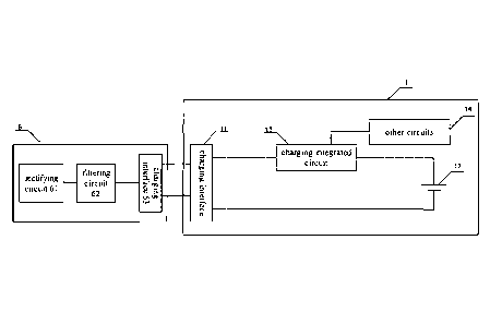
FIG 1 is a schematic diagram of a device to be charged and a relevant adapter
for charging
the device to be charged according to an example embodiment. As illustrated in
FIG 1, the device
1 includes: a charging interface 11, a battery unit 12, a charging integrated
circuit (IC) 13, and
other circuits 14.
The device 1 can be charged by an adapter 6 of 10W (5V/2A). The adapter 6
charges the
device 1 in the normal charging mode. The adapter 6 includes a rectifying
circuit 61, a filtering
circuit 62, and a charging interface 63. The rectifying circuit 61 is
configured to convert input AC
into DC, and the filtering circuit 62 is configured to perform a filtering
operation on the DC
outputted from the rectifying circuit 61 to provide stable DC to the device 1
coupled thereto
through the charging interface 63. The battery unit 12 may be, for example, a
single lithium battery
cell, and a charging cutoff voltage of the single cell is generally 4.2V.
Therefore, it is necessary to
arrange the charging integrated circuit 13 for converting voltage of 5V into
charging voltage
6
PI0E3195709PC A
CA 3068896 2020-01-31
suitable for the charging voltage expected by the battery unit 12. In
addition, the charging
integrated circuit 13 is also configured to supply power to other circuits 14
(such as a CPU or the
like) inside the device 1.
FIG. 2 is a schematic diagram of a device to be charged and a relevant adapter
for charging
the device to be charged according to an example embodiment. As illustrated in
FIG 2, the device
2 includes: a charging interface 21, a battery unit 22, a charging integrated
circuit (IC) 23, other
circuits 24, and a charging circuit 25.
The device 2 can be quickly charged by a high power adapter 7 of 20W (5V/4A),
in other
words, the adapter 7 charges the device 2 in the fast charging mode. The
adapter 7 includes a
rectifying circuit 71, a filtering circuit 72, a voltage conversion circuit
73, a control unit 74, and a
charging interface 75. The rectifying circuit 71 is configured to convert
input AC into DC. The
filtering circuit 72 is configured to perform a filtering operation on the DC
output from the
rectifying circuit 71 to provide stable DC. The voltage conversion circuit 73
is configured to
perform voltage conversion on the DC output from the filtering circuit 72. The
voltage conversion
circuit 73 is generally a step-down circuit for supplying DC of a suitable
voltage to the device 2
coupled thereto through the charging interface 75. The control unit 74 is
configured to receive
feedback from the device 2 to control the voltage and/or current of the DC
output from the
rectifying circuit 71. The charging circuit 25 is coupled to the charging
interface 21 and the battery
unit 22 for charging the battery unit 22. The battery unit 22 is still
exemplified by a lithium battery
including a single lithium battery cell. Since the voltage conversion circuit
73 is provided in the
adapter 7, the voltage output from the adapter 7 can be directly applied to
both ends of the battery
unit 22, that is, the charging circuit 25 charges the battery unit 22 in a
direct charging manner, and
the electric energy outputted by the adapter 7 is directly supplied to the
battery unit 22 through the
charging circuit 25 without voltage conversion. Optionally, the charging
circuit 25 can be a
switching circuit. The current output from the adapter 7 changes slightly in
voltage drop after
passing through the charging circuit 25 so as not to substantially affect the
charging process of the
battery unit 22. The charging integrated circuit 23 is configured to supply
power to the other
circuits 24 (such as a CPU or the like) inside the device 2.
In some embodiments, the adapter 7 can also provide the pulsating DC or the AC
to charge
the device 2. In order to realize the output of the pulsating DC or the AC of
the adapter 7, in an
embodiment, the foregoing filtering circuit 72 can be removed, so that the
unfiltered current output
7
PIOE3195709PCA
CA 3068896 2020-01-31
by the rectifying circuit 71 can directly supply power to the device 2 after
passing through the
voltage conversion circuit 73 and the charging interface 75. Alternatively,
the electrolytic capacitor
included in the aforementioned filtering circuit 72 may be removed to achieve
the output of the
pulsating DC or the AC.
In addition, the charging integrated circuit 23 can also control the adapter
to employ
multi-stage constant-current charging in the constant-current charging phase.
The multi-stage
constant-current charging may have M constant-current phases (M is an integer
no less than 2),
and the multi-stage constant-current charging starts from a first phase
charging with a preset
charging current, and the M constant-current phases are executed sequentially
from the first phase
to the Mth phase. When the previous constant-current phase in the constant-
current phases is
transferred to the next constant-current phase, the magnitude of the current
may be decreased.
When the battery voltage reaches a charging termination voltage threshold, the
previous
constant-current phase in the constant-current phases moves to the next
constant-current phase.
The current conversion process between two adjacent constant-current phases
may be gradual or
stepped.
For a device to be charged containing a single cell, when relatively-large
charging current is
used to charge the single cell, the heating phenomenon of the device to be
charged is more serious.
In order to ensure the charging speed of the device to be charged and to
alleviate the heating
phenomenon of the device to be charged during charging, the battery structure
can be modified,
and a plurality of cells coupled in series are used to be directly charged, in
other words, the voltage
output from the adapter is directly applied to both ends of the battery unit
containing multiple
cells. Compared with the single-cell solution (that is, the capacity of the
single cell before the
modifying is considered to be the same as the total capacity of the modified
multiple cells coupled
in series), if the same charging speed is achieved, the charging current
required for the multiple
cells is about 1/N of the charging current required for the single cell (N is
the number of cells in
series), in other words, multiple cells coupled in series can greatly reduce
the magnitude of the
charging current under the premise of ensuring the same charging speed,
thereby further reducing
the amount of heat generated by the device to be charged during charging.
FIG 3 is a schematic diagram of a device to be charged and a relevant adapter
for charging
the device to be charged according to an example embodiment. As illustrated in
FIG 3, the device
3 includes: a charging interface 31, a first battery unit 32, a second battery
unit 32', a charging
8
PI0E3195709PCA
CA 3068896 2020-01-31
integrated circuit 33, other circuits 34 and a charging circuit 35.
The device 3 can be quickly charged by a high power adapter 8 of 50W (10V/5A),
that is, the
adapter 8 charges the device 3 in the fast charging mode. The adapter 8
includes a rectifying circuit
81, a filtering circuit 82, a voltage conversion circuit 83, a control unit
84, and a charging interface
85. The rectifying circuit 81 is configured to convert input AC into DC. The
filtering circuit 82 is
configured to filter the DC output from the rectifying circuit 81 to provide
stable DC. The voltage
conversion circuit 83 is configured to perform voltage conversion on the DC
output from the
filtering circuit 82 to provide DC power of a suitable voltage to the device 3
coupled thereto
through the charging interface 85. The control unit 84 is configured to
receive feedback of the
device 3 to control the voltage and/or current of the DC output by the
rectifying circuit 81. The
first battery unit 32 is coupled in series with the second battery unit 32'.
The first battery unit 32
and the second battery unit 32' are, for example, both lithium batteries
including a single battery
cell. The charging circuit 35 is coupled to the charging interface 31 and the
first battery unit 32 and
the second battery unit 32' coupled in series for charging the first battery
unit 32 and the second
battery unit 32'. The voltage output from the adapter 8 can be directly
applied to both ends of the
first battery unit 32 and the second battery unit 32' coupled in series, in
other words, the charging
circuit 35 directly charges the first battery unit 32 and the second battery
unit 32' coupled in series
in a direct charging manner. It should be noted that, since the charging
circuit 35 charges the first
battery unit 32 and the second battery unit 32' coupled in series in the
direct charging manner, and
the line impedance causes a voltage drop in the charging circuit, the output
voltage output by the
adapter 8 and received by the charging circuit 35 is required to be greater
than the total voltage of
the multiple cells included in the first battery unit 32 and the second
battery unit 32'. In general,
the operating voltage of a single cell is between 3.0V and 4.35V. Taking the
dual cells coupled in
series as an example, the output voltage of the adapter 8 can be set to be
greater than or equal to
10V. The charging integrated circuit 33 is configured to supply power to other
circuits 34 (such as
a CPU or the like) inside the device 3.
In order to realize fast charging, the fast charging technology scheme with
high voltage and
small current as shown in FIGS. 4 and 5 can be adopted.
FIG 4 is a schematic diagram of a device to be charged according to an example
embodiment
As illustrated in FIG 4, the device 4 includes a charging interface 41, a
battery unit 42, a charging
integrated circuit 43, other circuits 44, and a switched-capacitor conversion
circuit 45.
9 PI
0E3195709PCA
CA 3068896 2020-01-31
=
The device 4 can be quickly charged, for example, by an adapter 9 having
maximum output
voltage of 10 V and supporting only a single cell. The switched-capacitor
conversion circuit 45 can
be, for example, a switched-capacitor DC-DC converter. The switched-capacitor
conversion circuit
45 is coupled to the charging interface 41 and the battery unit 42, and
receives the voltage output
from the adapter through the charging interface 41 to charge the battery unit
42. The battery unit
42 is still exemplified by a lithium battery including a single lithium
battery cell. Since the output
voltage of the adapter is 10 V, it cannot be directly loaded on both ends of
the battery unit 42.
Therefore, the switched-capacitor conversion circuit 45 is required as the
charging circuit of the
battery unit 42. The voltage output from the adapter is stepped down to meet
the expected charging
voltage of the battery unit 42. The charging integrated circuit 43 is
configured to supply power to
the other circuits 44 inside the device 4.
A device to be charged using a switched-capacitor conversion circuit can also
use a battery in
which a plurality of cells are coupled in series.
FIG 5 is a schematic diagram of a device to be charged according to an example
embodiment
of the present disclosure. As shown in FIG 5, the device 5 includes a charging
interface 51, a first
battery unit 52, a second charging unit 52', a charging integrated circuit 53,
other circuits 54, and a
switched-capacitor conversion circuit 55.
The device 5 can be quickly charged, for example, by an adapter 9' which
supports double
cells with maximum output voltage of 20V. The switched-capacitor conversion
circuit 55 can be,
for example, a switched-capacitor DC-DC converter. The switched-capacitor
conversion circuit 55
is coupled to the charging interface 51 and the first battery unit 52 and the
second charging unit 52'
coupled in series, and the voltage output by the adapter is received through
the charging interface
51 to charge the first battery unit 52 and the second charging unit 52'
coupled in series. Both the
first battery unit 52 and the second charging unit 52' are exemplified by a
lithium battery including
a single battery cell. Since the output voltage of the adapter is 20V, which
is greater than the total
voltage of the two cells in the first battery unit 52 and the second charging
unit 52', the
switched-capacitor conversion circuit 55 is required to perform step down on
the voltage output
from the adapter. The charging integrated circuit 53 is configured to supply
power to the other
circuits 54 inside the device 5.
A battery supply circuit, a device to be charged, and a charging control
method according to
the embodiments of the present disclosure are described as follows.
10
PI0E3195709PCA
CA 3068896 2020-01-31
,
FIG. 6 is a schematic diagram of a battery supply circuit according to an
example
embodiment.
As illustrated in FIG 6, the battery supply circuit 10 can be applied for a
device to be charged
(not shown in the figures), and includes a first cell 102, a second cell 104,
a switch 106, a first
switching unit 108, and a second switching unit 110.
A first end of the second cell 104 is coupled to a first end of the second
switching unit 110,
and a second end of the second cell 104 is coupled to a first end of the
switch 106, a second end of
the second switching unit 110 is coupled to a second end of the switch 106. A
first end of the first
cell 102 is coupled to the second end of the switch 106, a second end of the
first cell 102 is
coupled to a first end of the first switching unit 108, and a second end of
the first switching unit
108 is coupled to the first end of the switch 106. In FIG 6, the second end of
the first cell 102 is
taken as a grounding end, which is not limited in this disclosure.
In a case that the switch 106 is turned on, and the first switching unit 108
and the second
switching unit 110 are in an off state, the first cell 102 and the second cell
104 are coupled in
series, and in a case that the switch 106 is turned off, and the first
switching unit 108 and the
second switching unit 110 are in an on state, the first cell 102 and the
second cell 104 are coupled
in parallel.
FIG 7 is an equivalent circuit diagram of the battery supply circuit in a case
that the switch
106 is turned on, and the first switching unit 108 and the second switching
unit 110 are in an off
state. FIG 8 is an equivalent circuit diagram of the battery supply circuit in
a case that the switch
106 is turned off and the first switching unit 108 and the second switching
unit 110 are in an on
state.
In some embodiments, the first cell 102 and the second cell 104 each may be a
single cell or
each may be multiple cells coupled in series.
In some embodiments, the first cell 102 and the second cell 104 may be cells
in a plurality of
cells included in the device to be charged.
In some embodiments, the first cell 102 and the second cell 104 may be
packaged together in
a battery cell or in two batteries.
The current device to be charged (or components in the device to be charged or
chips in the
device to be charged) generally adopts a single cell for power supply.
Therefore, in a case that the
first cell 102 and the second cell 104 are coupled in series for charging, if
the first cell 102 or the
11
PI0E3195709PCA
CA 3068896 2020-01-31
,
second cell 104 is configured to supply power to the device to be charged (or
the components in
the device to be charged or the chips in the device to be charged), the cell
for power supply
continues to consume power, thus resulting in imbalanced voltage between the
first cell 102 and
the second cell 104 (or the voltages are inconsistent). The voltage imbalance
between the first cell
102 and the second cell 104 reduces the overall performance of the first cell
102 and the second
cell 104 and affects the service life of the first cell 102 and the second
cell 104. In addition, the
voltage imbalance between the first cell 102 and the second cell 104 may make
it difficult to
manage multiple cells in a unified manner. Therefore, the battery supply
circuit according to the
embodiment of the present disclosure also introduces an equalization circuit:
a first switching unit
108 and a second switching unit 110.
In some embodiments, the first switching unit 108 and the second switching
unit 110 are
switching tubes (e.g. MOS tubes, and CMOS tubes), At the end of charging, if
the voltage
difference between the first cell 102 and the second cell 104 is greater than
a first voltage
difference threshold, the first switching unit 108 and the second switching
unit 110 work in an
equilibrium state, and the first switching unit 108 and/or the second
switching unit 110 can be
controlled to operate in a linear region to provide a current-limiting
resistor (refer to the
current-limiting resistors R1 and R2 in FIG 7), thereby reducing the voltage
difference between
the first cell 102 and the second cell 104 to prevent large current from
damaging the battery when
the voltage difference between the two is large. When the voltage difference
between the first cell
102 and the second cell 104 is less than a second voltage difference threshold
(the second voltage
difference threshold is less than the first voltage difference threshold)
through equalization, the
first switching unit 108 and the second switching unit 110 are completely
turned on, so that the
first cell 102 and the second cell 104 are coupled in parallel.
According to the battery supply circuit provided by the embodiments of the
present
disclosure, a plurality of charging connection modes can be provided in the
device to be charged
through switch control. For example, when the first cell 102 and the second
cell 104 are coupled in
parallel for charging, both the normal charging scheme as shown in FIG. 1 and
the fast charging
scheme as shown in FIG. 2 or FIG. 4 are applicable for charging. When the
first cell 102 and the
second cell 104 are coupled in series for charging, the fast charging scheme
shown in FIG. 3 or
FIG 5 is applicable for charging.
FIG. 9 is a schematic diagram of a device to be charged according to an
example embodiment.
12
PI0E3195709PCA
CA 3068896 2020-01-31
The device 20 shown in FIG. 9 may be, for example, a terminal or a
communication terminal,
which includes but is not limited to a device configured to receive/transmit
communication signals
via a wired connection (for example, public switched telephone network (PSTN),
digital
subscriber line (DSL) connection, digital cable connection, direct cable
connection and/or another
.. data connection/network) and/or via a wireless interface (for example,
cellular network, wireless
local area network (WLAN), digital TV network such as digital video
broadcasting handheld
(DVB-H) network, satellite network, an amplitude modulation-frequency
modulation (AM-FM)
broadcasting transmitter, and/or a wireless interface of another communication
terminal). The
communication terminal configured to communicate via the wireless interface
may be referred to
as "wireless communication terminal", "wireless terminal" and/or "mobile
terminal". Examples of
mobile terminals include, but are not limited to a satellite phone or a cell
phone, a terminal
combining a cell radio phone and a personal communication system (PCS) having
capability of
data process, fax, and data communication, a personal digital assistant (PDA)
including a radio
phone, a pager, Internet/Intranet access, a web browser, a note pad & address
book, a calendar
and/or a global positioning system (GPS) receiver, and a common laptop and/or
handheld receiver,
or other electronic devices including a radio phone transceiver.
The device 20 includes the battery supply circuit 10 as shown in FIG 6
described above, a
charging interface 202, a first charging circuit 206, and a second charging
circuit 208.
It should be noted that, the embodiment of the present disclosure does not
specifically limit
.. the type of the charging interface 202. For example, the charging interface
202 may be a Universal
Serial Bus (USB) interface. The USB interface may be a standard USB interface,
a micro USB
interface or a Type-C interface. The first charging circuit 206 and/or the
second charging circuit
208 can charge the first cell 102 and the second cell 104 through a power line
in the USB
interface. The power line in the USB interface can be a VBus line and/or a
ground line in the USB
interface.
FIG. 10 is a circuit diagram in a case that a device 20 to be charged is
charged by a first
charging circuit 206 in a first charging mode according to an example
embodiment.
As shown in FIG 9 and FIG 10, FIG. 10 is a circuit diagram, in a case that the
switch 106
shown in FIG. 9 is turned off, and the device 20 is charged by the first
charging circuit 206 in the
first charging mode. The first charging mode may be, for example, the normal
charging mode as
shown in FIG. 1.
13
PI0E3195709PCA
CA 3068896 2020-01-31
,
The first charging circuit 206 can, for example, adopt a conventional charging
circuit design,
that is, a conversion circuit (such as a charging integrated circuit) is
provided between the charging
interface 202 and the first end of the first cell 102, so that the first cell
102 and the second cell 104
coupled in parallel can be charged. The conversion circuit can perform
constant voltage and
constant current control on the charging process of the adapter (such as the
adapter 6 shown in
FIG 1) for charging the device 20, and modulate the output voltage of the
adapter according to
actual needs, such as step-down. In some embodiments, the charging integrated
circuit may be, for
example, a Buck circuit.
In some embodiments, the first charging circuit 206 is also configured to
supply power to
other circuits 204 of the device 20, and may include a circuit management
module 2062 for
managing a charging circuit of the first cell 102 and the second cell 104 and
a charging circuit for
supplying power to the other circuits.
In the normal charging mode provided by the first charging circuit 206, the
adapter outputs a
relatively-small current value or uses relatively-small power to charge the
first cell 102 and the
second cell 104 coupled in parallel in the device 20.
FIG 11 is a circuit diagram in a case that a device 20 to be charged is
charged by a second
charging circuit 208 in a second charging mode according to an example
embodiment. FIG. 12 is a
circuit diagram in a case that a device 20 is charged by a second charging
circuit 208 in a third
charging mode according to an example embodiment.
As illustrated in FIG 9 and FIG 11, FIG 11 is a circuit diagram in a case that
the switch 106
shown in FIG 9 is turned off, and the device 20 is charged by the second
charging circuit 208 in
the second charging mode. The second charging mode may be, for example, the
fast charging
mode shown in FIG 2, that is, a high-power charging scheme of 20W (5V/4A). In
the second
charging mode provided by the second charging circuit 208, the second charging
circuit 208 may
adopt a direct charging manner as shown in FIG 2 to charge the first cell 102
and the second cell
104 coupled in parallel.
As illustrated in FIG 9 and FIG 12, FIG 12 is a circuit diagram in a case that
the switch 106
shown in FIG 9 is turned off, and the device 20 is charged by the second
charging circuit 208 in
the third charging mode. The third charging mode may be, for example, the fast
charging mode
shown in FIG 3, that is, a high-power charging solution of 50W (10V/5A). In
the third charging
mode provided by the second charging circuit 208, the second charging circuit
20 may adopt a
14
PI0E3195709PCA
CA 3068896 2020-01-31
direct charging manner as shown in FIG 3 to charge the first cell 102 and the
second cell 104
coupled in series.
The connection manner of the first cell 102 and the second cell 104 can be
controlled, for
example, based on a switch or a control unit. The switch or control unit can
be flexibly switched
between serial connection mode and parallel connection mode according to the
actual needs (such
as the type of adapter coupled).
In addition, as shown in FIG 12, in a case that the third charging mode is
adopted to charge
the first cell 102 and the second cell 104 through the second charging circuit
206, the first charging
circuit 206 is further configured to directly draw energy from the adapter to
supply power to the
other circuits 204 of the device 20; or, the electric energy output by a
positive electrode of the first
cell 102 can also be used to power the other circuits 204 through the first
charging circuit 106.
It should be noted that, in order to simplify the circuit diagram, the
equalization circuits in the
first cell 102 and the second cell 104 are not shown in FIG 12, but those
skilled in the art should
understand that when the series charging of the device 20 is completed, the
device 20 shown in
FIG 12 is configured to reduce the voltage difference between the first cell
102 and the second cell
104 according to the above-mentioned equalization method through the first
switching unit 108
and the second switching unit 110 before the first cell 102 and the second
cell 104 are coupled in
parallel.
FIG. 13 is a schematic diagram of a device to be charged according to an
example
embodiment.
As illustrated in FIG. 13, the difference between the device 30 and the device
20 shown in
FIG 9 is that the device 30 further includes: a control unit 302.
The control unit 302 may perform bidirectional communication with the adapter
for charging
the device 30 through a data line in a cable coupled to the charging interface
202 to negotiate a
charging mode between the adapter and the device 30. In addition, the control
unit 302 is further
configured to control a connection between the first cell 102 and the second
cell 104, that is, the on
and off of the control switch 106, and the status or work area of the first
switching unit 108 and the
second switching unit 110.
Taking the charging interface 202 as a USB interface as an example, the data
line may be a
D+ line and/or a D- line in the USB interface.
It should be noted that the above description of the present disclosure does
not limit the
15
PI0E3195709PCA
CA 3068896 2020-01-31
master-slave nature of the adapter and the control unit 302. In other words,
any one of the adapter
and the control unit 302 can initiate a bidirectional communication session as
the master device.
Accordingly, the other party may act as a slave device to make a first
response or a first reply to
the communication initiated by the master device. As a feasible method, during
the communication
process, the identity of the master and slave devices can be confirmed by
comparing the electrical
level of the adapter side and the side of the device to be charged with
respect to the ground.
The present disclosure does not limit the specific implementation of the
bidirectional
communication between the adapter and the control unit 302, that is, any one
of the adapter and
the control unit 302 can initiate a communication session as the master
device, and accordingly the
other party acts as the slave device to make a first response or a first reply
to the communication
initiated by the master device, and at the same time, the master device can
make a second response
to the first response or the first reply of the slave device, and it can be
considered that a negotiation
process of a charging mode between the master device and the slave device are
completed (also
called a "bidirectional communication" process between the master device and
the slave device).
As a feasible implementation mode, the master device and the slave device can
perform the
charging operation between the master device and the slave device after the
negotiation of multiple
charging modes is completed to ensure that the negotiated charging process is
safely and reliably
executed.
A first way in which the master device makes the second response to the first
response or first
reply to the communication session according to the policy of the slave device
can be: the master
device can receive the first response or first reply made by the slave device
for the communication
session, and make a targeted second response based on the received first
response or first reply of
the slave device. For example, when the master device receives the first
response or first response
of the slave device for the communication session within a preset time, the
master device responds
to the first response or first response of the slave device through the
targeted second response.
Specifically, the master device and the slave device have completed a
negotiation of the charging
mode, and the master device and the slave device perform a charging operation
in the first
charging mode or the second charging mode according to a negotiation result.
That is, the adapter
works in the first charging mode or the second charging mode to charge the
device to be charged
according to the negotiation result.
A second way in which the master device makes the second response to the first
response or
16
PI0E3195709PCA
CA 3068896 2020-01-31
first reply to the communication session according to the policy of the salve
device can be: the
master device does not receive the first response or first reply from the
slave device for the
communication session within the preset time, and the master device also makes
a targeted second
response to the first response or first reply of the slave device. For
example, when the master
device does not receive the first response or first reply of the slave device
for the communication
session within the preset time, the master device side also respond to the
first response or the first
response of the slave device through the targeted second response.
Specifically, the master device
and the slave device have completed the negotiation of a charging mode, and
the master device
and the slave device perform a charging operation in the first charging mode,
that is, the adapter
works in the first charging mode to charge the device to be charged.
When the device 30 to be charged initiates a communication session as a master
device, and
the adapter as a slave device makes a first response or first reply to the
communication session
initiated by the master device, there is no need for the device 20 to be
charged to respond to the
first response or first reply made by the adapter with a targeted second
response, it is considered
that the adapter and the device 30 to be charged have completed the
negotiation of a charging
mode, and it can be further determined according to the negotiation result
that the first cell 102 and
the second cell 104 are charged by the first charging circuit 206 or the
second charging circuit 208.
In some embodiments, the control unit 302 performs bidirectional communication
with the
adapter through a data line to negotiate a charging mode between the adapter
and the device to be
charged. In detail, the control unit 302 receives a first instruction sent by
the adapter, and the first
instruction is configured to query whether the device 30 turns on a third
charging mode. The
control unit 302 sends a reply instruction of the first instruction to the
adapter, and the reply
instruction of the first instruction is configured to indicate whether the
device 30 agrees to turn on
the third charging mode. In a case that the device 30 agrees to turn on the
third charging mode, the
control unit 302 is further configured to control the adapter to charge the
first cell 102 and the
second cell 104 through the second charging circuit 208, and control the first
cell 102 and the
second cell 104 to be coupled in series, and control the first charging
circuit 206 to be coupled to
the adapter, so that the first charging circuit 206 draws energy from the
adapter when supplying
power to other circuits of the device 30.
In some embodiments, the control unit 302 performs bidirectional communication
with the
adapter through a data line to negotiate a charging mode between the adapter
and the device to be
17
PI0E3195709PCA
CA 3068896 2020-01-31
charged. In detail, the control unit 302 receives a second instruction sent by
the adapter, and the
second instruction is configured to query whether the device 30 turns on a
second charging modes.
The control unit 302 sends a reply instruction of the second instruction to
the adapter, and the reply
instruction of the second instruction is configured to indicate whether the
device 30 agrees to turn
on the second charging mode. In the case that the device 30 agrees to turn on
the second charging
mode, the control unit 302 is further configured to control the adapter to
charge the first cell 102
and the second cell 104 through the second charging circuit 208, and control
the first cell 102 and
the second cell 104 to be coupled in parallel.
In some embodiments, the control unit 302 performs bidirectional communication
with the
adapter through a data line to negotiate a charging mode between the adapter
and the device to be
charged. In detail, according to the first instruction, the reply instruction
of the first instruction, the
second instruction and the reply instruction of the second instruction, in the
case where the device
30 neither agrees to turn on the second charging mode nor agrees to turn on
the third charging
mode, the control unit 302 is also configured to control the adapter to charge
the first cell 102 and
the second cell 104 through the first charging circuit 206, and control the
first cell 102 and the
second cell 104 to be coupled in parallel.
FIG 14 is a schematic diagram of a device to be charged according to an
example
embodiment.
As illustrated in FIG 14, the device 40 includes the battery supply circuit
10, the charging
interface 202, and the first charging circuit 206 as shown in FIG 6 described
above, and a third
charging circuit 402.
FIG 15 is a circuit diagram in a case that the device 40 is charged by a third
charging circuit
402 in a fourth charging mode according to an example embodiment. FIG 16 is a
circuit diagram
in a case that the device 40 is charged by a third charging circuit 402 in a
fifth charging mode
according to an example embodiment.
As illustrated in FIG 14 and FIG 15, FIG 15 is a circuit diagram in a case
that the switch 106
shown in FIG 14 is turned off, and the device 40 is charged by the third
charging circuit 402 in the
fourth charging mode. The fourth charging mode may be, for example, the fast
charging mode
shown in FIG 4, that is, a high-power charging scheme with an adapter output
voltage of 10V. In
the fourth charging mode provided by the third charging circuit 402, the third
charging circuit 402
includes, for example, a switched-capacitor DC-DC converter, and adopts a
charging method as
18
PI0E3195709PCA
CA 3068896 2020-01-31
shown in FIG 4, to charge the first cell 102 and the second cell 104 in
parallel.
As illustrated in FIG 14 and FIG 16, FIG 16 is a circuit diagram in a case
that the switch 106
shown in FIG 14 is turned off, and the device 40 is charged by the third
charging circuit 402 in the
fifth charging mode. The fifth charging mode may be, for example, the fast
charging mode shown
in FIG 5, that is, a high-power charging scheme with an adapter output voltage
of 20V. In the fifth
charging mode provided by the third charging circuit 402, the third charging
circuit 402 includes,
for example, a switched-capacitor DC-DC converter, which adopts a charging
method shown in
FIG 5 to charge the first cell 102 and the second cell 104 coupled in series.
It should be noted that, in order to simplify the circuit diagram, the
equalization circuit in the
first cell 102 and the second cell 104 is not shown in FIG 16, but those
skilled in the art should
understand that when the series charging is completed, the device 40 shown in
FIG 16 is
configured to reduce the voltage difference between the first cell 102 and the
second cell 104
according to the above-mentioned equalization method above-mentioned the first
switching unit
108 and the second switching unit 110 before the first cell 102 and the second
cell 104 are coupled
in parallel.
In some embodiments, the device 40 further includes a control unit 302'.
Bidirectional
communication is performed between the control unit 302' and the adapter
through a data line to
negotiate the charging mode between the adapter and the device to be charged.
In detail, the
control unit 302' receives a third instruction sent by the adapter, and the
third instruction is
configured to query whether the device 30 turns on the fifth charging mode.
The control unit 302'
sends a reply instruction of the third instruction to the adapter, and the
reply instruction of the third
instruction is configured to indicate whether the device 30 agrees to turn on
the fifth charging
mode. In the case where the device 30 agrees to turn on the fifth charging
mode, the control unit
302' is further configured to control the adapter to use the switched-
capacitor converter 402 to
charge the first cell 102 and the second cell 104, and to control the first
cell 102 and the second
cell 104 to be coupled in series.
In some embodiments, bidirectional communication is performed between the
control unit
302' and the adapter through a data line to negotiate the charging mode
between the adapter and
the device to be charged. In detail, the control unit 302' receives a fourth
instruction sent by the
adapter, and the fourth instruction is configured to query whether the device
30 turns on the fourth
charging mode. The control unit 302' sends a reply instruction of the fourth
instruction to the
19
PI0E3195709PCA
CA 3068896 2020-01-31
adapter, and the reply instruction of the fourth instruction is configured to
indicate whether the
device 30 agrees to turn on the fourth charging mode. In the case where the
device 30 agrees to
turn on the fourth charging mode, the control unit 302' is further configured
to control the adapter
to use the switched-capacitor converter 402 to charge the first cell 102 and
the second cell 104,
and to control the first cell 102 and the second cell 104 to be coupled in
parallel.
The device to be charged according to the present disclosure may provide the
battery supply
circuit, and the battery supply circuit is capable of accommodating various
charging schemes, e.g.
a normal charging mode and a fast charging mode, a flash charging mode (e.g.
the second charging
mode described above) and a super-flash charging mode (e.g. the third charging
mode described
above) in the fast charging mode. Moreover, for different charging modes,
power may be supplied
through two batteries that can be coupled in parallel or charging integrated
circuit in the device to
be charged. This manner does not cause loss by power conversion, and can
further improve the
cruising ability of the device to be charged. In addition, based on the
bidirectional communication
with the adapter, the device to be charged can automatically switch to
different charging modes
according to the type of the adapter, which can improve the using experience
of the user.
It should be noted that the block diagrams shown in the above drawings are
functional entities
and do not necessarily correspond to physically or logically independent
entities. These functional
entities may be implemented in the form of software, or implemented in one or
more hardware
modules or integrated circuits, or implemented in different networks and/or
processor devices
and/or microcontroller devices.
The following are method embodiments of the present disclosure. For details
not disclosed in
the method embodiments of the present disclosure, please refer to the device
embodiments of the
present disclosure.
FIG 17 is a flowchart of a charging control method according to an example
embodiment.
The charging method is used for charging a device to be charged. The device to
be charged
includes: a charging interface and any one of the power supply circuits 20,
30, or 40 described
above.
As illustrated in FIG 17, the charging control method 50 includes the
following acts.
At block S502, the switch in the supply circuit is turned on and the first
switching unit and
the second switching unit in the supply circuit are caused to be in an off
state in response to
receiving a first control instruction, such that the first cell and the second
cell are coupled in series
20
PI0E3195709PCA
CA 3068896 2020-01-31
=
in the supply circuit.
At block S504, the switch is turned off and the first switching unit and the
second switching
unit are caused to be in an on state in response to receiving a second control
instruction, such that
the first cell and the second cell are coupled in parallel.
In some embodiments, the charging control method 50 includes: in a case that
the first cell
and the second cell are coupled in series for charging, after the charging is
completed, determining
whether a voltage difference between the first cell and the second cell is
greater than a first voltage
difference threshold; in response to that the voltage difference between the
first cell and the second
cell is greater than the first voltage difference threshold, controlling the
first switching unit and/or
the second switching unit to operate in a linear region to provide a current-
limiting resistor for the
first cell and/or the second cell; and in response to that the voltage
difference between the first cell
and the second cell is less than a second voltage difference threshold,
controlling the first
switching unit and the second switching unit to operate in a conducting state;
and in which the
second voltage difference threshold is less than the first voltage difference
threshold.
In some embodiments, the charging control method 50 includes: receiving an
output voltage
and an output current of an adapter through the charging interface.
In some embodiments, the device to be charged includes: a charging integrated
circuit. The
method further includes: causing the battery supply circuit to supply power to
other circuits of the
device to be charged by the charging integrated circuit.
In some embodiments, the charging control method 50 includes: converting the
output
voltage by the charging integrated circuit, and applying the converted output
voltage on both ends
of the first cell and the second cell coupled in parallel in the battery
supply circuit.
In some embodiments, the charging control method 50 includes: directly
applying the output
voltage and the output current on both ends of the first cell and the second
cell coupled in series in
the battery supply circuit, or directly applying the output voltage and the
output current on both
ends of the first cell and the second cell coupled in parallel in the battery
supply circuit.
In some embodiments, the charging control method 50 includes: in response to
directly
applying the output voltage and the output current on both ends of the first
cell and the second cell
coupled in series, supplying power the other circuits by the charging
integrated circuit using
voltage on the first cell.
In some embodiments, the charging control method 50 includes: in response to
directly
21
PI0E3195709PCA
CA 3068896 2020-01-31
applying the output voltage and the output current on both ends of the first
cell and the second cell
coupled in series, drawing energy from the adapter to charge the other
circuits by the charging
integrated circuit.
In some embodiments, the adapter supports a first charging mode, a second
charging mode,
and a third charging mode; in the first charging mode, the charging integrated
circuit applies the
converted output voltage on both ends of the first cell and the second cell
coupled in parallel in the
battery supply circuit; in the second charging mode, the charging integrated
circuit directly applies
the output voltage and the output current on both ends of the first cell and
the second cell coupled
in parallel in the battery supply circuit; and in the third charging mode, the
charging integrated
circuit directly applies the output voltage and the output current on both
ends of the first cell and
the second cell coupled in series in the battery supply circuit.
In some embodiments, the charging interface includes a data line, and the
method further
includes: performing bidirectional communication with the adapter through the
data line to
negotiate the charging mode between the adapter and the device to be charged.
In some embodiments, performing bidirectional communication with the adapter
through the
data line to negotiate the charging mode between the adapter and the device to
be charged,
includes: receiving a first instruction sent by the adapter, in which the
first instruction is
configured to query whether the device to be charged turns on the third
charging mode; and
sending a reply instruction of the first instruction to the adapter, in which
the reply instruction of
the first instruction is configured to indicate whether the device to be
charged agrees to turn on the
third charging mode.
In some embodiments, the charging control method 50 includes: in response to
that the device
to be charged agrees to turn on the third charging mode, sending the first
control instruction.
In some embodiments, performing bidirectional communication with the adapter
through the
data line to negotiate the charging mode between the adapter and the device to
be charged,
includes: receiving a second instruction sent by the adapter, in which the
second instruction is used
to query whether the device to be charged turns on the second charging mode;
and sending a reply
instruction of the second instruction to the adapter, in which the reply
instruction of the second
instruction is in response to that to indicate whether the device to be
charged agrees to turn on the
second charging mode.
In some embodiments, the charging control method 50 includes: in response to
that the device
22
PI0E3195709PCA
CA 3068896 2020-01-31
to be charged agrees to turn on the second charging mode, sending the second
control instruction.
In some embodiments, the device to be charged further includes a switched-
capacitor
converter, and the method further includes: converting the output voltage by
the
switched-capacitor converter, and directly applying the converted output
voltage on both ends of
the first cell and the second cell coupled in series in the battery supply
circuit, or directly applying
the converted output voltage on both ends of the first cell and the second
cell coupled in parallel in
the battery supply circuit.
In some embodiments, the charging control method 50 includes: in a case that
the
switched-capacitor converter directly applies the output voltage and the
output current on both
ends of the first cell and the second cell coupled in series, charging the
other circuits by the
charging integrated circuit using voltage on the first cell.
In some embodiments, the charging control method 50 includes: in a case that
the
switched-capacitor converter directly applies the output voltage and the
output current on both
ends of the first cell and the second cell coupled in series, drawing energy
from the adapter to
charge the other circuits by the charging integrated circuit.
In some embodiments, the adapter supports a fourth charging mode and a fifth
charging
mode; in the fourth charging mode, the switched-capacitor converter applies
the converted output
voltage on both ends of the first cell and the second cell coupled in parallel
in the battery supply
circuit; in the fifth charging mode, the switched-capacitor converter applies
the converted output
voltage on both ends of the first cell and the second cell coupled in series
in the battery supply
circuit.
In some embodiments, the charging interface includes a data line, the method
further
includes: performing bidirectional communication with the adapter through the
data line to
negotiate the charging mode between the adapter and the device to be charged.
In some embodiments, performing bidirectional communication with the adapter
through the
data line to negotiate the charging mode between the adapter and the device to
be charged
comprises: receiving a third instruction sent by the adapter, in which the
third instruction is
configured to query whether the device to be charged turns on the fifth
charging mode; and
sending a reply instruction of the third instruction to the adapter, in which
the reply instruction of
the third instruction is configured to indicate whether the device to be
charged agrees to turn on the
fifth charging mode.
23
PI0E3195709PCA
CA 3068896 2020-01-31
,
In some embodiments, the charging control method 50 includes: in a case that
the device to
be charged agrees to turn on the fifth charging mode, sending the first
control instruction.
In some embodiments, performing bidirectional communication with the adapter
through the
data line to negotiate the charging mode between the adapter and the device to
be charged,
comprises: receiving a fourth instruction sent by the adapter, in which the
fourth instruction is
configured to query whether the device to be charged turns on the fourth
charging mode; and
sending a reply instruction of the fourth instruction to the adapter, in which
the reply instruction of
the fourth instruction is configured to indicate whether the device to be
charged agrees to turn on
the fourth charging mode.
In some embodiments, the charging control method 50 includes: in a case that
the device to
be charged agrees to turn on the fourth charging mode, sending the second
control instruction.
With the charging control method according to the embodiments of the present
disclosure, it
is possible to perform charging control for the device to be charged that has
a battery supply circuit
applicable for various charging schemes. Based on bidirectional communication
with the adapter,
different charging modes can be switched according to the type of the adapter,
thereby improving
the user experience.
It should be noted that the above-mentioned drawings are merely a schematic
description of
processes included in the method according to the exemplary embodiment of the
present
disclosure, and are not for limiting purposes. It is easy to understand that
the processes shown in
the above drawings do not indicate or limit the chronological order of these
processes. In addition,
it is also easy to understand that these processes may be, for example,
performed synchronously or
asynchronously in multiple modules.
The exemplary embodiments of the present disclosure have been particularly
shown and
described above. It should be understood that the present disclosure is not
limited to the detailed
structure, arrangement, or implementation method described herein; rather, the
present disclosure
is intended to cover various modifications and equivalent arrangements
included within the spirit
and scope of the appended claims.
24
PI0E3195709PCA
CA 3068896 2020-01-31