Note: Descriptions are shown in the official language in which they were submitted.
CA 03069156 2020-01-06
WO 2019/014052
PCT/US2018/041002
TECHNIQUES FOR LASER ABLATION/SCRIBING OF COATINGS IN
PRE- AND POST-ASSEMBLED INSULATED GLASS UNITS, AND/OR
ASSOCIATED METHODS
TECHNICAL FIELD
[0001] Certain example embodiments of this invention relate to
techniques for laser ablation/scribing of coatings in pre- and post-laminated
assemblies, pre- and post-assembled insulated glass units, and/or other
products, as well as associated methods. More particularly, certain example
embodiments of this invention relate to techniques for laser ablating/scribing
peripheral edges of a coating (e.g., a low-emissivity, mirror, or other
coating)
on a glass or other substrate in a pre- or post-laminated assembly, pre- or
post-
assembled insulated glass unit, and/or other product, in order to slow or
prevent
corrosion of the coating, and/or associated products.
BACKGROUND AND SUMMARY
[0002] Laminated products have been used in a variety of applications
including, for example, low-emissivity (low-E), mirror, and other
applications.
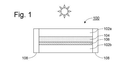
Fig. 1 is a cross-sectional view of an example laminated product 100. The Fig.
1 example laminated product 100 includes first and second substantially
parallel, spaced-apart substrates (e.g., glass substrates) 102a and 102b,
laminated together with a laminating material 104, also sometimes called an
interlayer. Typical laminating materials include, for example, PVB, EVA,
PET, PU, and the like. Depending on the application, the laminating material
104 may be optically "clear," i.e., it may have a high visible transmission.
One
or more coatings may be formed on one or more major surfaces of the first
substrate 102a and/or the second substrate 102b. For example, it is not
uncommon to include a low-E, mirror, antireflection (AR), or other coating on
the second or third surface of a laminated product. In some instances, a
coating
1
CA 03069156 2020-01-06
WO 2019/014052
PCT/US2018/041002
may be provided to each of the second and third surfaces. For ease of
understanding, Fig. 1 includes an example coating 106 on surface 3. An
optional additional edge seal 108 may be provided around a periphery of the
article 100, and the edge seal 108 may be intended to protect the side edges
of
the article 100, the laminating material 104, the coating 106, etc., from
mechanical, environmental, and/or other types of damage.
[0003] One problem with laminated products is that laminated metal
layer inclusive thin films and laminated metallic layer inclusive thin films,
such
as those oftentimes used in mirror and low-E coatings, can gradually corrode
from the edge to the center of the lite, e.g., when exposed to gradients in
temperature, humidity, etc. Corrosion happens in presence and ingress of
ionized moisture. Edge defects in the lamination process and a lack of edge
deletion, can also trigger corrosion. Although edge sealants can be used to
reduce the likelihood of the advance of the corrosion front, such techniques
may not be practical, as these sealants can also develop cracks over time.
[0004] Edge deletion generally involves removing a portion of the
coating around peripheral edges of the underlying substrate, and edge deletion
tables are known. See, for example, U.S. Patent Nos. 4,716,686; 5,713,986;
5,934,982; 6,971,948; 6,988,938; 7,125,462; 7,140,953; and 8,449,348, each of
which is hereby incorporated herein in its entirety. In general, in such
tables, a
series of casters provided to the table allow for smooth movement of glass
across the surface of the table. Grinding wheels of various widths may be used
in connection with shields to help reduce the scattering of debris and for
safety
purposes. Passing the glass substantially consistently under the deletion head
efficiently "deletes" the coating from the glass so that it can be used, for
example, in connection with the above-described and/or other articles. Wider
or narrower grinding wheels may be used to delete more or less coating from
the glass surface.
[0005] Although edge deletion tables can be used in a variety of
applications, they unfortunately have their limitations, especially when it
2
CA 03069156 2020-01-06
WO 2019/014052
PCT/US2018/041002
comes to corrosion prevention. For example, edge deletion tables oftentimes
are large and require additional machinery in a process line. The addition of
process steps can increase processing time and costs. Edge deletion tables, by
their nature, can also create debris that needs to be dealt with accordingly.
Thus, although edge deletion can sometimes remove edge defects, it also can
cause them by virtue of the creation of additional debris.
[0006] Moreover, although edge deletion tables oftentimes are suitable
for edge deletion, as their name implies, they oftentimes are limited in the
ability to remove coatings in interior areas. This can become increasingly
problematic as the area(s) to be removed become smaller and smaller, as there
is a practical limit to the size reductions possible for grinding wheels and
the
like. And because edge deletion tables function on exposed surfaces, they can
do nothing to "fix" already-assembled products and must be used early and in a
potentially disadvantageous time in a process line.
[0007] Certain example embodiments address these and/or other
concerns. For example, certain example embodiments relate to techniques for
stopping or at least slowing the advancement of the corrosion or delamination
edge-front relative to a coating in a laminated product.
[0008] Certain example embodiments are based on the recognition, from
work on soft low-E coatings, that electrochemical corrosion, driven by both
stress and ionized moisture ingress, is a main thermodynamic force behind this
phenomenon. Based on this recognition, certain example embodiments seek to
electrically isolate the coating from the edge, while simultaneously shunting
the layers and de-stressing the stack. In this regard, certain example
embodiments include laser-scribing the edge of a metal layer inclusive coating
or metallic layer inclusive coating on a cladded laminate. As one example,
laser-scribing of the coating through the laminate may be performed using a
diode fiber laser operating at 1064 nm. By optimizing or at least tuning the
width and position of the scribe with respect to glass edge, film corrosion
can
be either stopped or retarded. The viability of the laser scribe technique is
3
CA 03069156 2020-01-06
WO 2019/014052
PCT/US2018/041002
related to the fact that glass substrates and many laminating materials
(including PVB, which is very commonly used) are transparent to 1064 nm
laser irradiation and thus cannot be etched directly (or at least cannot
easily be
etched directly with certain lasers including, for example, 1064 nm lasers).
[0009] In certain example embodiments, a method of making a
laminated product is provided. An intermediate product includes first and
second substantially parallel glass substrates that are laminated together
with a
laminating material, with the first glass substrate having had a multilayer
thin
film coating formed thereon, and with the coating including at least one metal-
inclusive layer and being susceptible to corrosion. In making the laminated
product, a line is laser-scribed in the coating by exposing the intermediate
product to a laser source, with the line creating a barrier to electron
transport
between opposing sides thereof.
[0010] In certain example embodiments, a method of making a
laminated product is provided. A multilayer thin film coating is formed on a
first glass substrate, with the coating including at least one metal-inclusive
layer and being susceptible to corrosion. The first glass substrate is
laminated
to a second glass substrate using a laminating material so that the coating is
oriented between the first and second substrates and so that the first and
second
substrates are substantially parallel to one another. Following the
laminating,
and in making the laminated product, a border line is laser-scribed around a
periphery of the coating. The laser-scribing at least partially dissolves the
coating proximate to the border line and increases electrochemical corrosion
resistance of the coating internal to the border line by electrically
isolating the
coating internal to the border line. Dissolved material from the coating, by
virtue of the laser-scribing, is (a) incorporated into the first substrate,
laminating material, and/or an underlayer of the coating, and/or (b) ablated
and/or vaporized so as to re-form in a non-conductive manner.
[0011] In certain example embodiments, a laminated product is
provided. A first glass substrate supports a multilayer thin film coating. The
4
CA 03069156 2020-01-06
WO 2019/014052
PCT/US2018/041002
coating includes at least one metal-inclusive layer and is susceptible to
corrosion. A second glass substrate is laminated to the first glass substrate
using a laminating material so that the coating is oriented between the first
and
second substrates and so that the first and second substrates are
substantially
parallel to one another. A laser-scribed border is formed around a periphery
of
the coating formed after the first and second substrates have been laminated
together. At least the at least one metal-inclusive layer of the coating
proximate to the border is dissolved by virtue of the laser-scribing.
Dissolved
material from the coating, by virtue of the laser-scribing, is (a)
incorporated
into the first substrate, laminating material, and/or an underlayer of the
coating,
and/or (b) ablated and/or vaporized so as to re-form in a non-conductive
manner. The border has a width and depth sufficient to electrically isolate an
area internal to the border from an area external to the border to a level
sufficient to at least retard electrochemical corrosion in the area internal
to the
border.
[0012] In certain example embodiments, a kit for making a laminated
product. The kit includes a laser source and an intermediate product including
first and second substantially parallel glass substrates that are laminated
together with a laminating material, with the first glass substrate having had
a
multilayer thin film coating formed thereon, and with the coating including at
least one metal-inclusive layer and being susceptible to corrosion. The laser
source is controllable to laser-scribe a line in the coating by exposing the
intermediate product to a laser source in making the laminated product, with
the line creating a barrier to electron transport between opposing sides
thereof.
[0013] In certain example embodiments, a method of making a
laminated product comprises: having an intermediate product, the intermediate
product including first and second substantially parallel glass substrates
that are
laminated together with a laminating material, the first glass substrate
having
had a multilayer thin film coating formed thereon, the coating including at
least
one metal-inclusive layer; and coupling energy into the coating by exposing
the
CA 03069156 2020-01-06
WO 2019/014052
PCT/US2018/041002
intermediate product to a laser from a laser source operating at a wavelength
at
which the second glass substrate and the laminating material are substantially
transmissive in making the laminated product, the energy being coupled into
the coating and the laser source being controlled so as to selectively cause
at
least a part of the coating, in a desired pattern, to (a) dissolve into the
first
substrate, the laminating material, and/or an underlayer of the coating,
and/or
(b) vaporize and re-form in a manner that does not conduct, the desired
pattern
defining at least first and second areas and being formed to a width and depth
sufficient to electrically isolate the first and second areas from one
another, the
electrical isolation being at a level sufficient to at least substantially
retard
electrochemical corrosion in the first area.
[0014] In a similar respect, certain example embodiments relate to IG
units made in the same or similar manners. For instance, in certain example
embodiments, a method of making an IG unit is provided. An intermediate
product includes first and second substantially parallel spaced apart glass
substrates that are connected together with a peripheral edge spacer. A gap is
defined between the first and second substrates. The first glass substrate has
a
multilayer thin film coating formed thereon. The coating includes at least one
metal-inclusive layer and being susceptible to corrosion. A line is laser-
scribed
in the coating by exposing the intermediate product to a laser source in
making
the IG unit, with the line creating a barrier to electron transport between
opposing sides thereof.
[0015] In certain example embodiments, a method of making an IG unit
is provided. On a first glass substrate, a multilayer thin film coating is
formed,
with the coating including at least one metal-inclusive layer and being
susceptible to corrosion. The first glass substrate is connected to a second
glass
substrate in connection with a peripheral edge spacer so that the coating is
oriented between the first and second substrates and so that the first and
second
substrates are substantially parallel to, and spaced apart from, one another.
Following the connecting, a border line is laser-scribed around a periphery of
6
CA 03069156 2020-01-06
WO 2019/014052
PCT/US2018/041002
the coating in making the IG unit. The laser-scribing at least partially
dissolves
the coating proximate to the border line and increases electrochemical
corrosion resistance of the coating internal to the border line by
electrically
isolating the coating internal to the border line. At least the at least one
metal-
inclusive layer is dissolved, by virtue of the laser-scribing, such that
associated
ablated material is (a) re-formed in a non-conductive manner, and/or (b)
dissolved and/or diffused into the first substrate and/or at least one other
layer
of the multilayer thin film coating.
[0016] In certain example embodiments, an IG unit is provided. A first
glass substrate supports a multilayer thin film coating, with the coating
including at least one metal-inclusive layer and being susceptible to
corrosion.
A second glass substrate is substantially parallel to and spaced apart from
the
first glass substrate, with the coating being oriented between the first and
second substrates. An edge seal is included. A laser-scribed border around a
periphery of the coating is formed after the first and second substrates have
been connected together. At least the at least one metal-inclusive layer of
the
coating proximate to the border is dissolved by virtue of the laser-scribing.
Dissolved material from the coating, by virtue of the laser-scribing, is (a)
incorporated into the first substrate and/or an underlayer of the coating,
and/or
(b) ablated and/or vaporized so as to re-form in a non-conductive manner. The
border has a width and depth sufficient to electrically isolate an area
internal to
the border from an area external to the border to a level sufficient to at
least
retard electrochemical corrosion in the area internal to the border.
[0017] In certain example embodiments, a kit for making an IG unit is
provided. The kit includes a laser source and an intermediate product. The
intermediate product includes first and second substantially parallel spaced
apart glass substrates that are connected together with a peripheral edge
spacer,
a gap being defined between the first and second substrates, the first glass
substrate having had a multilayer thin film coating formed thereon, the
coating
including at least one metal-inclusive layer and being susceptible to
corrosion.
7
CA 03069156 2020-01-06
WO 2019/014052
PCT/US2018/041002
The laser source is controllable to laser-scribe a line in the coating by
exposing
the intermediate product to a laser source in making the IG unit, the line
creating a barrier to electron transport between opposing sides thereof.
[0018] In certain example embodiments, a method of making an IG unit
is provided, with the method comprising: having an intermediate product, the
intermediate product including first and second substantially parallel spaced
apart glass substrates that are connected together with a peripheral edge
spacer,
a gap being defined between the first and second substrates, the first glass
substrate having had a multilayer thin film coating formed thereon, the
coating
including at least one metal-inclusive layer; and coupling energy into the
coating by exposing the intermediate product to a laser from a laser source
operating at a wavelength at which the second glass substrate is substantially
transmissive in making the IG unit, the energy being coupled into the coating
and the laser source being controlled so as to selectively cause at least a
part of
the coating, in a desired pattern, to (a) dissolve into the first substrate
and/or an
underlayer of the coating, and/or (b) vaporize and re-form in a manner that
does not conduct, the desired pattern defining at least first and second areas
and
being formed to a width and depth sufficient to electrically isolate the first
and
second areas from one another, the electrical isolation being at a level
sufficient
to at least substantially retard electrochemical corrosion in the first area.
[0019] In a similar respect, certain example embodiments relate to a
coated article including a substrate supporting a multilayer thin film coating
and/or a method of making the same. The thin film coating is laser scribed so
as to create at least first and second areas, the first and second areas being
electrically isolated form one another by virtue of the laser scribing. The
laser
scribing may be performed when the coating of the coated article is in a
closed
or open geometry relative to the coated article and/or anything into which it
might be built.
[0020] The features, aspects, advantages, and example embodiments
described herein may be combined to realize yet further embodiments.
8
CA 03069156 2020-01-06
WO 2019/014052
PCT/US2018/041002
BRIEF DESCRIPTION OF THE DRAWINGS
[0021] These and other features and advantages may be better and more
completely understood by reference to the following detailed description of
exemplary illustrative embodiments in conjunction with the drawings, of
which:
[0022] FIGURE 1 is a cross-sectional view of an example laminated
product;
[0023] FIGURE 2 schematically illustrates one example corrosion
mechanism;
[0024] FIGURE 3 is a schematic cross-sectional view of an example
low-emissivity coating that sometimes encounters corrosion problems;
[0025] FIGURE 4 is a schematic view of a laser scribing setup that may
be used in connection with certain example embodiments;
[0026] FIGURE 5 shows scribe lines obtained with a 1064 nm nano-
second pulsed laser, which may be used in connection with certain example
embodiments;
[0027] FIGURE 6 is a first example setup showing how a laminated
article can be laser scribed in accordance with certain example embodiments;
[0028] FIGURE 7 is a second example setup showing how a laminated
article can be laser scribed in accordance with certain example embodiments;
[0029] FIGURE 8 is a flowchart showing an example process for laser-
scribing a laminated article in accordance with certain example embodiments;
[0030] FIGURE 9 is a cross-sectional view of an example insulated glass
unit (IG unit or IGU) that may have a coating laser ablated in accordance with
certain example embodiments; and
[0031] FIGURE 10 is a flowchart showing an example process for laser-
scribing an IG unit in accordance with certain example embodiments.
9
CA 03069156 2020-01-06
WO 2019/014052
PCT/US2018/041002
DETAILED DESCRIPTION
[0032] Certain example embodiments relate to techniques for laser
ablating/scribing peripheral edges of a metal layer inclusive or metallic
layer
inclusive coating (e.g., a low-emissivity, mirror, or other coating) on a
glass or
other substrate in a pre- or post-laminated assembly, insulated glass unit (IG
unit or IGU), or other product, in order to slow or prevent corrosion of the
coating, and/or associated products. Certain example embodiments may be
used in connection with products having coatings that have already started to
erode, e.g., even after such products have been installed (for example, in a
building, vehicle, etc.).
[0033] Corrosion can be thought of as the deterioration of materials by
chemical processes. One subset is electrochemical corrosion of metals, in
which the oxidation process M ¨> M + e- is facilitated by the presence of a
suitable electron acceptor. At the electron acceptor site, an in-series
resistance,
called polarization resistance, develops. The magnitude of this resistor
affects
the rate of corrosion. One characteristic of most corrosion processes is that
the
oxidation and reduction steps occur at separate locations on the metal. This
is
possible because metals are conductive, so the electrons can flow through the
metal from the anodic to the cathodic regions. The presence of water aids in
transporting ions to and from the metal, but a thin film of adsorbed moisture
can be sufficient to enable corrosion.
[0034] Thus, it will be appreciated that a corrosion system can be
regarded as a short-circuited electrochemical cell including anodic and
cathodic
steps that follow general patterns. For example, the anodic process may
resemble something like:
M(s) ¨> Mx+ (aq) + xe-
The cathodic processes can be any of:
CA 03069156 2020-01-06
WO 2019/014052
PCT/US2018/041002
02+ 2H20 + 4e- ¨> 40H-
+ e- ¨>1/2H2(g)
Mlx+ + xe- ¨> Ml(s)
where MI is another metal.
[0035] Many currently available low-E coatings include a layer
comprising Ag directly on and contacting a layer comprising ZnO and directly
under and contacting a layer comprising Ni (e.g., a layer comprising NiCr,
NiTi, or an oxide thereof). In such systems, from a simplistic thermodynamic
modeling perspective, layers with electrochemical potentials lower than that
of
Ag will "preferentially" corrode. A layer comprising Ni, for example, will
start
to corrode very quickly relative to a layer comprising Ag and, in such
systems,
the entire interface therebetween can be compromised. On the other hand,
when a layer comprising ZnO and a layer comprising Ag are considered, the
situation is reversed, as the layer comprising Ag will corrode faster (both
with
and without light). A layer comprising NiO also will "outperform" the layer
comprising Ag. Of course, this model assumes completion of the electrical
circuit and the role of H20 providing the fr ions in the presence of
electrolytes
such as, for example, salts.
[0036] Several standard electrode potentials are given in the following
table, in volts relative to the standard hydrogen electrode:
Half-Reaction
E (V)
Oxidant Reductant
Ni2+ + 2e- Ni(s) -0.25
Ag+ + e- Ag(s) +0.7996
Ni02(s) + 4H+ + 2e- # Ni2+ + 20H- +1.59
11
CA 03069156 2020-01-06
WO 2019/014052
PCT/US2018/041002
[0037] Other commonly available low-E coatings involve a layer
comprising Ag sandwiched between and directly contacting layers comprising
NiCr. (Specific example coatings of this type will be discussed in greater
detail
below.) Based on electrochemical potentials, in such coatings, the corrosion
of
the metallic Ni present in the NiCr-inclusive barrier layers that surround the
Ag
will result in an "adhesive release" and subsequent agglomeration of the
silver,
which is one of the fingerprints of electrochemical corrosion. An electrolyte
containing water in electrical contact with both metals will exacerbate the
"preferential" corrosion of the Ni and, eventually, lead to corrosion of the
Ag.
[0038] Fig. 2 schematically illustrates this corrosion mechanism. As
shown in Fig. 2, a layer comprising Ag 202 is sandwiched between first and
second layers comprising NiCr 204a and 204b. An electrolyte 206 (in water) is
in contact with these layers. Electrons will migrate into the layer comprising
Ag 202, while there will be preferential leaching of Ni2+ from one or both
layers comprising NiCr 204a / 204b into the electrolyte 206. The overall
mechanism results in the "preferential" dissolution and re-deposition of
(corroded) Ni, together with the agglomeration or "clotting" of Ag.
[0039] Still other commonly available low-E coatings involve a layer
comprising zinc oxide (e.g., a layer comprising zinc oxide which may include
aluminum, tin, and/or the like), a layer comprising Ag formed on (optionally
directly on an in direct physical contact with) the layer comprising zinc
oxide,
and a layer comprising Ni, Cr, and/or Ti, or an oxide thereof (e.g., NiCr,
NiCrOx, NiTi, NiTiOx, etc.) formed on (optionally directly on an in direct
physical contact with) the layer comprising Ag. In layer stacks comprising
ZnOx/Ag/NiCrOx, relatively small and oxidized Ni present suggested a
different mechanism of Ag corrosion, with nominally no interfacial release
which, as evidenced from testing and analysis, was significantly less visually
objectionable.
[0040] When placed in an electrolyte (e.g., salt plus H20), split Ag
layer
stacks (e.g., where the same metallic structure material is used but split
12
CA 03069156 2020-01-06
WO 2019/014052
PCT/US2018/041002
spatially with dielectrics that are electrically active) can develop
differences in
potential as a result of biaxial stress becoming interfacial stress; metal
grain
composition; imperfections, scratches, threads, etc., being exposed;
electrolyte
gradient in the dielectric, laminating PVB or other material, etc.; and/or the
like.
[0041] In so-called double silver low-E products, one of the two silver
layers can start to corrode preferentially with respect to the other, mediated
by
the electrolyte gradient in the electrically active dielectric, which acts as
a
polarization layer. This is similar to a battery setting up a voltage
difference as
a result of a chemical potential imbalance. One of the Ag layers becomes
anodic with respect to the remainder of the stack, and the other Ag will
preferentially corrode. However, here this action occurs where the dielectric
integrity is compromised and water vapor can get into the layers. The water
vapor transmission rate (WVTR) thus can become an important parameter.
The electrochemical model predicts that if there is no ionized moisture
ingress,
the corrosion front should not move.
[0042] In a related regard, the electrochemical model of corrosion makes
some other predictions that can be useful for future designs, namely, that the
thickness ratio of the Ag to NiCr ratio also affects propensity of corrosion.
Surprisingly, modelling also predicts that the ionic conductivity/polarization
of
the glass can help reduce corrosion. Thus, a thinner underlayer or an ionic
underlayer should help reduce corrosion.
[0043] To help assess the models, consider Fig. 3, which is a cross-
sectional view of an example low-E layer stack arrangement. As shown in Fig.
3, a substrate 300 supports a first silicon-inclusive layer 302a (e.g., a
layer
comprising silicon and an oxide and/or nitride thereof); a first layer
comprising
Ni, Cr, and/or Ti 304a (which may or may not be oxidized); a layer comprising
silver 306; a second layer comprising Ni, Cr, and/or Ti 304b (which may or
may not be oxidized); and a second silicon-inclusive layer 302b (e.g., a layer
comprising silicon and an oxide and/or nitride thereof). The following three
13
CA 03069156 2020-01-06
WO 2019/014052 PCT/US2018/041002
example layer thickness correspond to layers with different visual appearances
and/or low-E and other performance:
Example 1
Layer Preferred More Preferred Example
Thickness (nm) Thickness (nm) Thickness (nm)
Si3N4 (302b) 385 ¨ 525 405 ¨ 505 455
NiCr (304b) 20 ¨ 30 22 ¨ 28 25
Ag (306) 95 ¨ 135 100 ¨ 130 115
NiCr (304a) 30 ¨ 50 35 ¨ 45 40
Si3N4 (302a) 110 ¨ 150 115 ¨ 145 130
Glass (300) N/A N/A N/A
Example 2
Layer Preferred More Preferred Example
Thickness (nm) Thickness (nm) Thickness (nm)
Si3N4 (302b) 435 ¨ 595 460 ¨ 570 515
NiCr (304b) 25 ¨ 35 27 ¨ 33 30
Ag (306) 105 ¨ 145 110 ¨ 140 125
NiCr (304a) 20 ¨ 30 22 ¨ 28 25
Si3N4 (302a) 235 ¨ 325 250 ¨ 310 280
Glass (300) N/A N/A N/A
Example 3
Layer Preferred More Preferred Example
Thickness (nm) Thickness (nm) Thickness (nm)
Si3N4 (302b) 360 ¨ 490 380 ¨ 470 425
NiCr (304b) 30 ¨ 50 35 ¨ 45 40
Ag (306) 55 ¨ 75 58 ¨ 72 65
14
CA 03069156 2020-01-06
WO 2019/014052
PCT/US2018/041002
NiCr (304a) 35 ¨ 55 40 ¨ 50 45
Si3N4 (302a) 260 ¨ 360 280 ¨ 340 310
Glass (300) N/A N/A N/A
[0044] Considering the three examples above, Example 3 has the
thickness undercoat (e.g., the layer comprising Si3N4 302a), and it seemingly
has the greatest propensity for corrosion. Example 1 has the thinnest
undercoat
(e.g., the layer comprising Si3N4 302a), and it seemingly smallest propensity
for corrosion. There are, however, additional or alternative hypotheses as to
why these phenomena are encountered. First, it is possible that the undercoat
(e.g., the layer comprising Si3N4 302a) in Example 3 may be rougher than the
corresponding layers in the other coatings, potentially caused by its greater
thickness, and potentially leading to poorer interfacial adhesion and in turn
leading to corrosion more easily. Second, there may be greater tensile
strength
in the Example 3 undercoat (e.g., the layer comprising Si3N4 302a). TEM
imaging and/or other tests may help evaluate the former, and stress-modified
layer depositions achieving the same total thicknesses may help evaluate the
latter. As suggested above, however, it is possible that these hypotheses may
work individually or collectively to account for the relative ease of
corrosion.
In any event, regardless of the precise corrosion-facilitating mechanism at
play,
the example techniques set forth herein operate to slow down and potentially
eliminate corrosion from occurring.
[0045] In this regard, because both the cathodic and anodic steps must
take place for corrosion to occur, prevention of either one should stop
corrosion. It might be possible to stop both processes by coating the object
with a humidity barrier or other protective coating. However, even if this is
done, there are likely to be places where the barrier is broken or does not
penetrate, particularly if there are holes in the structure. A more
sophisticated
approach is to apply a slight negative charge to the metal, thus making it
more
CA 03069156 2020-01-06
WO 2019/014052
PCT/US2018/041002
difficult for the M ¨> M2+ + 2e- reaction to take place. If the film is
encapsulated so that there is a gradient in humidity and oxygen from the
periphery and center of the film, a yet more elegant approach involves
inducing
an equipotential scribe line that helps set up an extremely large polarization
resistance. These approaches may be used in any suitable combination, in
different example embodiments of this invention.
[0046] In this later regard, laser scribing experiments, in connection
with
a diode fiber laser at 1064 nm and through various glass thicknesses, were
performed. An X-Y scanner heled guide the laser over the substrates, resulting
in locally-isolated spots or continuous lines where overlapping spots were
used.
The focus plane and beam diameter (e.g., the size of the beam at the coating
depth) was adjusted using optics in the laser head coupled with pre-determined
gap spacers. In these experiences, the substrates were assumed to be
transparent or at least substantially transparent (e.g., at least 85%
transmissive,
more preferably at least 90% transmissive, and still more preferably 95% or
more transmissive) at 1064 nm, and coupling of the laser was targeted for the
coating.
[0047] Fig. 4 is a schematic view of a laser scribing setup that may be
used in connection with certain example embodiments. The setup includes a
laser 402 that sits atop a platform 404 and a column 406. The platform is
movable in X-Y directions via an X-Y movement stage 408a, and in the Z
direction via the Z movement stage 408b. Both the X-Y movement stage 408a
and the Z movement stage 408b may be computer controllable, e.g., to focus
light emitted from the laser 402 relative to the slotted sample stage 410 and
the
substrate 412 thereon. Output from the laser 402 is directed along a fixed-
length tube towards first optics 416a, which redirects the output along a
second
tube 414b. Focusing and/or other optics 416b focuses the output from the laser
402 through the nozzle 414c and towards the slotted sample stage 410 and the
substrate 412 thereon. A coolant jet 418 is provided to help cool the
substrate
16
CA 03069156 2020-01-06
WO 2019/014052
PCT/US2018/041002
412 and/or components thereof (e.g., a coating therein or thereon, laminating
material, and/or the like).
[0048] The laser can be controlled by adjusting the scan speed, pulse
frequency / duty cycle, and/or the diode output power. The depth of focus also
may be taken into account. These and/or other parameters may be adjusted
using the structure noted above (e.g., the optics, stages, etc.). Scan speeds
may
range from 250-2000 mm/s, more preferably 500-1000 mm/s. Discrete "low"
and "high" scan speeds may operate at, for example, 500 mm/s and 100 mm/s,
respectively, in certain example embodiments. Pulse frequencies may range
from 10-240 kHz, more preferably 20-160 kHz, and still more preferably 40-80
kHz. Discrete "low", "medium", and "high" pulse frequencies usable in
connection with certain example embodiments are 40 kHz, 60 kHz, and 80
kHz, respectively. For a top glass substrate thickness of 3-4 mm (e.g., the
glass
substrate closest to the laser source), a diode laser power of 50-250 uJ, more
preferably 75-200 uJ, and still more preferably 75-150 uJ, may be used.
Furthermore, a beam diameter or major distance of 20-500 um, more preferably
20-250 um, and still more preferably 50-150 um, may be used. A beam radius,
for example, may be adjusted via the optics on the laser output, to have these
and/or other characteristics. In certain example embodiments, a beam diameter
of about 100 um delivering a laser power pulse at or just about 100 uJ (e.g.,
100-115 uJ) may be particularly advantageous for 4 mm glass. In order to
optimize or improve the scribing process for the particular coating, the laser
power and pulse frequency may be adjusted to provide, as an approximate
center point, these values. Scribe lengths of 1-24 inches, and sometimes even
shorter or longer are possible, with a scribe length of 12 inches being one
example that has been found to work with certain example embodiments. As
one example, operating at 5-15% of an 80W power source for an 1064 nm laser
has been found to be sufficient for certain example embodiments.
17
CA 03069156 2020-01-06
WO 2019/014052
PCT/US2018/041002
[0049] The depth of focus may be varied to target the top of the
coating,
the bottom of the coating, or the metallic layer(s) of the coating in
different
example embodiments.
[0050] In certain example embodiments, pulse energy and movement
can be used to create scribing spot overlaps. In this regard, Fig. 5 shows
scribe
lines obtained with a 1064 nm nano-second pulsed laser, which may be used in
connection with certain example embodiments. In Fig. 5, a 100 uJ pulse at a
frequency of 20-80 kHz with a laser beam diameter of about 100 um was used.
The lines moving from left-to-right show the effects of increasing spot
overlaps. As can be seen, the conductivity is reduced with further overlaps.
Multi-pass scribing (e.g., scribing with two or more lines on top of each
other)
may be used in certain example embodiments. In certain example
embodiments, the scribe line width preferably will be at least 100-300 um,
although a 500-800 um scribe line width would be more preferable. In certain
example embodiments, one, two, three, or more scribe lines that are generally
parallel to one another could be advantageously used to create successive
electron transport barrier zones. In certain example embodiments, one or more
line, dot, or other laser types may be used to form the scribes. Line lasers
may
be particularly advantageous in certain example embodiments, e.g., based on
their ability to directly target lines. It will be appreciated that overlaps
may be
used with line, dot, and/or other laser types, in different example
embodiments.
[0051] Fig. 6 is a first example setup showing how a laminated article
can be laser scribed in accordance with certain example embodiments, and Fig.
7 is a second example setup showing how a laminated article can be laser
scribed in accordance with certain example embodiments. Figs. 6 and 7
include laminated products similar to that shown in and described in
connection with Fig. 1. That is, in Figs. 6 and Fig. 7, first and second
substrates
602a and 602b are laminated together using a laminating material / interlayer
604 (which may be PVB, EVA, PET, PU, and the like. The first substrate 602a
supports a coating 606 (e.g., the coating from the Fig. 3 example, another
18
CA 03069156 2020-01-06
WO 2019/014052
PCT/US2018/041002
coating as described herein, or some other coating having a metal or metallic
layer and being susceptible to corrosion).
[0052] As shown in Fig. 6, energy 610 from a laser source is focused on
the coating 606 and coupled into the metal and/or metallic layer(s) therein.
As
shown in Fig. 7, energy 710a from a laser source is redirected and focused on
the coating 606 with the aid of additional optics 712. The redirected and
focused energy 710b is coupled into the metal and/or metallic layer(s) in the
Fig. 7 example. In addition to the presence of additional optics 712 in Fig. 7
compared to Fig. 6, Fig. 6 and Fig. 7 differ from one another in terms of
their
orientations relative to the laser sources (not shown). That is, the coating
606
is closer to the laser source than is the laminating layer 604 in Fig. 6,
whereas
the coating 606 is farther from the laser source than is the laminating layer
604
in Fig. 7. It is noted that certain example embodiments may use additional
optics regardless of the position of the coating and laminating material
relative
to the laser source.
[0053] Certain example embodiments may implement an ablation
approach that is selective and "self-regulating" in terms of depth, e.g.,
because
of differences in absorption, thermo-mechanical properties of the substrate
and
the layers involved in the stack, and/or the like. One example of a self-
regulating approach would involve the removal of both Ag and NiCr inclusive-
layers, as well as the interlayers, from the Fig. 3 example coating, using
(for
example) a diode laser operating at a wavelength that is not absorbed by the
underlying and overlying layers (which, in the Fig. 3 example, are layers
comprising silicon nitride) and that is not absorbed by the substrate(s).
[0054] One challenge, however, relates to the fact that the target
product
has a closed geometry; that is, there is a question as to where the ablated
material will go. This concern may be addressed in one or more of several
ways. For example, ablated material may be vaporized but then re-form (e.g.,
re-deposit) in a manner that does not conduct. Alternatively, or in addition,
ablated material from the coating may be allowed to dissolve into the
substrate
19
CA 03069156 2020-01-06
WO 2019/014052
PCT/US2018/041002
itself, into one or more thin film layers on the substrate (e.g., the layer
comprising silicon nitride 302a in the Fig. 3 example), etc. Additionally, or
alternatively, in a similar fashion, ablated material may be transferred into
molten or at least softened laminating material (e.g., PVB), e.g., by
diffusing or
dissolving into it.
[0055] It will be appreciated, however, that potential damage or even
ablation of the substrate may be problematic in some instances, as it may
induce damage to an insulating or barrier layer between the substrate and the
metal or metallic layer(s) in the coating (e.g., silicon-inclusive
underlayers,
bottom dielectric layers, and/or the like). Thus, certain example embodiments
may operate at a power level and with a duty cycle sufficient to generate heat
and/or otherwise cause the laminating material to at least partially soften so
that
the ablated material has a place to go, preferably without causing damage to
the
substrate underlying the coating and also preferably without causing removal
of
the barrier layer between the metal or metallic layer(s) in the coating and
the
underlying substrate. In this regard, the Fig. 7 orientation may be
comparatively easier to work with, as ablating the bottom surface of the
laminating material to cause energy to couple into the coating and
preferentially target the metal or metallic layer(s) therein may be "safer,"
e.g.,
in terms of reducing or eliminating the exposure of the barrier layer and back
contact to laser radiation. In certain example embodiments, it nonetheless may
be desirable to cut through an entire coating.
[0056] If the contour of the laser scribe is too sharp or too jagged
(i.e.,
the local radius curvature of the laser scribe profile is too sharp), then the
cut in
the PVB or laminating material may not be wide enough. This in turn will
affect the polarization resistance and the series resistance. A straight line
with
no sharp bends may be preferable. In certain example embodiments, corners
thus may be handled using overlapping straight lines (e.g., resulting in a
plus-
or cross-like arrangement at corners), using gradual curves (e.g., which may
be
"gone over" multiple times to ensure that proper grooves are formed), etc.
CA 03069156 2020-01-06
WO 2019/014052
PCT/US2018/041002
[0057] It has been found that the distance between the scribe line and
the
edge of the substrate can have an effect on whether and to what extent
electrochemical corrosion can be slowed and/or stopped. For example, if the
distance between the edge of the substrate and the scribe line is low,
electrochemical corrosion can be slowed but not stopped. A distance of at
least
3mm, more preferably at least 5mm, and still more preferably at least lOmm is
advantageous when it comes to not only slowing corrosion, but also to
increasing the likelihood of corrosion being stopped.
[0058] Fig. 8 is a flowchart showing an example process for laser-
scribing a laminated article in accordance with certain example embodiments.
A coating is formed on a substrate in step S802, with the coating being (for
example) a multilayer thin film coating including at least one metal or
metallic
layer. The substrate with the coating thereon is laminated to another
substrate
using a laminating material in step S804. The laminated article is exposed to
a
laser source so that the coating is ablated in step S806. An optional outer
seal
is provided in step S808, so as to further protect the laminated article.
[0059] In this way, it is possible to laser-scribe / ablate a coating
through
glass and a laminating material or interlayer (such as PVB or the like) as a
way
to simulate edge deletion and also create a zone that serves as a barrier for
electron transport between the edge of the coating and the center of the
coating.
By selecting parameters such as the width of the scribe, the power of the
laser,
the duty cycle, the wavelength of the laser, etc., it is possible to control
the
ablation and diffusion of the coating into the glass, PVB, and/or one or more
other layers of the thin film coating. In so doing, electrochemical corrosion
can
be slowed or stopped. That is, the coating can be electrically isolated from
the
external environment to reduce and sometimes completely eliminate stray
leakage currents that contribute to the eventual electrochemical erosion of
the
coating. Certain example embodiments are sufficient to provide for sub-pico A
electrical isolation (e.g., electrical isolation less than 10 pico A, more
preferably less than 1 pico A). That is, the corrosion rate may be decreased
by
21
CA 03069156 2020-01-06
WO 2019/014052
PCT/US2018/041002
orders of magnitude by accordingly increasing the series (Rs) and polarization
resistance (Rp), and decreasing the shunt resistance. It is noted that the
example techniques described herein may be used to electrically decouple areas
such that the DC resistance between them is above the 30 gigaohm limit of
conventional electrometer measuring devices and therefore can be taken as
infinite in some sense.
[0060] As suggested above, a high-quality edge sealant may be used to
provide additional protection, but the laser scribing can provide yet better
insensitivity to weathering elements in at least some respects, e.g., by
reducing
and sometimes completely eliminating interface current carrying elements to
the environment along which moisture can enter and leakage current can exit.
This improvement is possible even in the presence of a laminate, which
otherwise tends to increase the leakage current by orders of magnitude by
virtue of moisture in the laminate (e.g., as PVB in contrast to EVA transmits
that moisture) and is responsible for a broad range of life-limiting
degradation
effects related to electrochemical corrosion. Certain example embodiments
advantageously reduce the likelihood of intra-cohesive failures of the coating
stack, e.g., related to electrochemical corrosion related to potential
differences
in which anodic metallization dissolves and cathodic metallization usually
dominates.
[0061] The laser scribing advantageously raises the internal resistance
of
the electrochemical corrosion path to the environment by orders of magnitude.
It is estimated that it is possible to realize a more than six order of
magnitude
decrease in leakage current in some instances. Moreover, the deeper and wider
the scribe line is, the higher the resistance is likely to be. Electrical
isolation
also decouples the regime from ground and changes the standard electrical
potential. The laser scribing of certain example embodiments advantageously
also advantageous affects the polarization resistance. The higher this value
is,
the more the corrosion kinetics will be slowed. Still further, the laser
scribing
22
CA 03069156 2020-01-06
WO 2019/014052
PCT/US2018/041002
of certain example embodiments advantageously also can involve shunting two
metallization layers so that their Fermi levels are at the same potentials.
[0062] Certain example embodiments have been described in connection
with a 1064 nm laser. A 1064 nm laser has been found to be advantageous,
because clear glass and PVB (and other laminating materials) are essentially
transparent to such wavelengths. By contrast, some lower and some higher
wavelength laser sources might heat the glass to too great of an extent, which
could cause cracks and/or other damage to the glass. It is noted, however,
that
clear glass is not always used in all applications. Green and other tinted
glasses, for example, are used in a number of different products in the U.S.
and
around the world, e.g., to obtain desired aesthetic affects. In such
instances,
1064 nm wavelength light may be absorbed by or otherwise ineffectively
coupled to the coating and, thus, it may be desirable to select a different
wavelength laser source. For green glass, for example, a 540 nm or 420 nm
wavelength laser may be desirable.
[0063] The scribe lines may be provided at the periphery of the products
in certain example embodiments. As a result, mounting structures, decorative
details, and/or the like may be used to obscure potentially resultant visible
artifacts of the scribing. In example embodiments where multiple scribe lines
are used, thicker scribe lines may be used closer to the periphery of the
article,
whereas thinner scribe lines may be used closer to the center of the article.
Doing so could help ensure that more aesthetically displeasing or at least
noticeable areas are covered.
[0064] In certain example embodiments, the example techniques
described herein can be used to create patterns in metal- and metallic-layer
inclusive coatings that can be routed to connectors outside of the glass.
[0065] It will be appreciated that the techniques of certain example
embodiments may be used in connection with a handheld or portable laser
source. The handheld or portable laser source may be used to scribe already-
installed, distributed, or other products that are not suitable for in-line or
23
CA 03069156 2020-01-06
WO 2019/014052
PCT/US2018/041002
manufacturing area adjustment, to impart electrochemical corrosion resistance
properties. The handheld or portable laser source may be mounted to a stage or
other blocking to as to facilitate controlled movement in two directions.
Range-finding optics may be provided so that the source may be positioned at
an appropriate distance from the product to facilitate focus on or proximate
to
the surface(s) to be treated.
[0066] In this vein, and in other scenarios as well, certain example
embodiments can also work in connection with some already corroded areas.
As will be appreciated from the description above, in common circumstances
(e.g., including clear glass substrates, PVB laminating materials, etc.), when
operating at a wavelength of 1064 nm, the laser's power will be absorbed first
by the metal and/or metallic layer(s). This energy is then transferred via
phonon coupling to the PVB or other laminating material and glass. Thus, if
the laser scribing is performed in already-corroded areas, the absorption of
the
laser may not be high enough (as the metal is already corroded) to create an
isolation channel in the PVB or other laminating material (i.e., the resistor
in
the electrochemical corrosion path). Thus, additional power may be needed.
However, care may be taken to ensure that sufficient active or passive cooling
is implemented, e.g., to reduce the likelihood of unwanted damage to the
substrate and/or adjacent areas of the PVB or other laminating material.
[0067] Additionally, laser scribing in a corroded area may not provide
an
area of equipotential. In other words, a voltage difference may still exist in
a
laser-scribed corroded area, although this may not be enough to drive the
corrosion front further. In some situations, the corrosion front may be driven
further, albeit at very slow rate.
[0068] Thus, it will be appreciated that it is possible in at least some
instances to scribe in already-corroded areas. However, the efficacy of doing
so may vary.
[0069] Although certain example embodiments have been described as
relating to laminated articles that have already been assembled, it will be
24
CA 03069156 2020-01-06
WO 2019/014052
PCT/US2018/041002
appreciated that the scribing techniques disclosed herein may be used in
connection with pre-laminated assemblies and, furthermore, in connection with
coated articles that may be incorporated into products other than laminated
products. For example, the scribing techniques disclosed herein may be used in
connection with coated articles, insulated glass units (IG units) where first
and
second substantially parallel spaced apart substrates are separated in
connection
with an edge seal defining a gap therebetween (which may be filled with air
and/or a noble gas such as Ar, Kr, Xe, and/or the like), vacuum insulated
glass
(VIG units) where first and second substantially parallel spaced apart
substrates
are separated in connection with an edge seal and a plurality of spacers with
a
gap being evacuated to a pressure less than atmospheric, etc.
[0070] In this regard, Fig. 9 is a cross-sectional view of an example IG
unit 900 that may have a coating laser ablated in accordance with certain
example embodiments, and Fig. 10 is a flowchart showing an example process
for laser-scribing an IG unit in accordance with certain example embodiments.
Fig. 9 is similar to Figs. 1 and 6-7, and Fig. 10 is similar to Fig. 8, except
that
Figs. 9-10 relate to techniques for IG units, whereas Figs. 1, 6-7, and 9
relate to
techniques for laminated products. In any event, referring more particularly
to
Figs. 9-10, first and second substrates 902a and 902b are provided for the IG
unit 900. A multilayer thin film coating 906, which may comprise one or more
metal-inclusive layers (e.g., in connection with a low-E or other coating) is
formed on the first substrate 902a (step S1002 in Fig. 10). The first and
second
substrates 902a and 902b are connected together (step S1004 in Fig. 10) using
peripheral edge spacer 910 and at least partially forming a gap 904. The IG
unit 900 is exposed to a laser source so that the coating 906 is ablated (step
S1006 in Fig. 10). The laser source may be oriented over the second substrate
902b, e.g., so as to reduce the likelihood of damaging the surface of the
first
substrate 902a. An optional outer seal 908 is provided (step S1008 in Fig.
10),
so as to further protect the IG unit 900.
CA 03069156 2020-01-06
WO 2019/014052
PCT/US2018/041002
[0071] It is noted that certain example embodiments may in essence help
c`ruggedize" the coating and/or product, making it less susceptible by
corrosion,
without completely scribing lines. For example, if the laser power is
controlled
in a manner such that scribing does not occur but instead laser power is
coupled
into the coating, then the metal-inclusive layer(s) may be altered such that
the
sheet resistance drops. This type of reduction in sheet resistance may not
create completely electrically isolated areas, but the sheet resistance
reductions
in the metal-inclusive layer(s) and/or coating as a whole may retard
advancement of the corrosion front, etc.
[0072] As used herein, the terms "on," "supported by," and the like
should not be interpreted to mean that two elements are directly adjacent to
one
another unless explicitly stated. In other words, a first layer may be said to
be
"on" or "supported by" a second layer, even if there are one or more layers
therebetween.
[0073] In certain example embodiments, a method of making an IG unit
is provided. An intermediate product includes first and second substantially
parallel spaced apart glass substrates that are connected together with a
peripheral edge spacer. A gap is defined between the first and second
substrates. The first glass substrate has a multilayer thin film coating
formed
thereon. The coating includes at least one metal-inclusive layer and being
susceptible to corrosion. A line is laser-scribed in the coating by exposing
the
intermediate product to a laser source in making the IG unit, with the line
creating a barrier to electron transport between opposing sides thereof.
[0074] In addition to the features of the previous paragraph, in certain
example embodiments, the laser source may be a 1064 nm laser source.
[0075] In addition to the features of either of the two previous
paragraphs, in certain example embodiments, the laser source may be operated
at a wavelength at which the second substrate is at least 90% transmissive.
[0076] In addition to the features of any of the three previous
paragraphs, in certain example embodiments, the coating may be a low-
26
CA 03069156 2020-01-06
WO 2019/014052
PCT/US2018/041002
emissivity coating including a layer comprising Ag. For instances, the coating
may be formed: (a) so as to include at least one layer comprising Ni, Cr,
and/or
Ti, the at least one layer comprising Ni, Cr, and/or Ti being formed on and in
physical contact with the layer comprising Ag; (b) so that the layer
comprising
Ag is sandwiched between and in direct physical contact with first and second
layers comprising Ni, Cr, and/or Ti; and/or (c) so that the layer comprising
Ag
is formed on an in direct physical contact with a layer comprising zinc oxide.
[0077] In addition to the features of any of the four previous
paragraphs,
in certain example embodiments, the laser-scribing may be performed (a) to
completely dissolve the coating proximate to the line; (b) to dissolve only a
part of the coating proximate to the line; or (c) to dissolve at least a part
of the
coating proximate to the line, material from the dissolved part of the coating
being re-deposited such that it does not conduct.
[0078] In addition to the features of any of the five previous
paragraphs,
in certain example embodiments, the coating may comprise a bottom dielectric
layer directly on the first glass substrate and the laser-scribing may be
performed to dissolve a portion of the coating including the at least one
metal-
inclusive layer but excluding the bottom dielectric layer. For instance, in
certain example embodiments, the dissolved portion of the coating may be at
least partially dissolved into the bottom dielectric layer.
[0079] In addition to the features of any of the six previous
paragraphs,
in certain example embodiments, heat generated by laser-scribing may be
controlled to avoid damaging the surface of substrate on which the coating is
formed. For instance, in certain example embodiments, the laser-scribing may
be interrupted and the intermediate product may be cooled and/or allowed to
cool during the interruption, in order to assist in controlling the generated
heat.
Additionally, or in the alternative, for instance, in certain example
embodiments, the duty cycle and/or operating power of the laser source may be
controlled in order to assist in controlling the generated heat.
27
CA 03069156 2020-01-06
WO 2019/014052
PCT/US2018/041002
[0080] In addition to the features of any of the seven previous
paragraphs, in certain example embodiments, the line may have a width of at
least 100-800 um.
[0081] In addition to the features of any of the eight previous
paragraphs, in certain example embodiments, the line may be formed around a
periphery of the intermediate article, e.g., with the barrier being defined
around
the periphery of the intermediate article.
[0082] In addition to the features of any of the nine previous
paragraphs,
in certain example embodiments, the laser-scribing may be practiced in
connection with multiple overlapping scans of the laser source.
[0083] In addition to the features of any of the 10 previous paragraphs,
in certain example embodiments, the laser-scribing may be performed to create
a sub 10 pico-A electrical isolation barrier.
[0084] In addition to the features of any of the 11 previous paragraphs,
in certain example embodiments, the second substrate may be oriented closer to
laser source than first substrate during the laser-scribing.
[0085] In certain example embodiments, a method of making an IG unit
is provided. On a first glass substrate, a multilayer thin film coating is
formed,
with the coating including at least one metal-inclusive layer and being
susceptible to corrosion. The first glass substrate is connected to a second
glass
substrate in connection with a peripheral edge spacer so that the coating is
oriented between the first and second substrates and so that the first and
second
substrates are substantially parallel to, and spaced apart from, one another.
Following the connecting, a border line is laser-scribed around a periphery of
the coating in making the IG unit. The laser-scribing at least partially
dissolves
the coating proximate to the border line and increases electrochemical
corrosion resistance of the coating internal to the border line by
electrically
isolating the coating internal to the border line. At least the at least one
metal-
inclusive layer is dissolved, by virtue of the laser-scribing, such that
associated
ablated material is (a) re-formed in a non-conductive manner, and/or (b)
28
CA 03069156 2020-01-06
WO 2019/014052
PCT/US2018/041002
dissolved and/or diffused into the first substrate and/or at least one other
layer
of the multilayer thin film coating.
[0086] In certain example embodiments, an IG unit is provided. A first
glass substrate supports a multilayer thin film coating, with the coating
including at least one metal-inclusive layer and being susceptible to
corrosion.
A second glass substrate is substantially parallel to and spaced apart from
the
first glass substrate, with the coating being oriented between the first and
second substrates. An edge seal is included. A laser-scribed border around a
periphery of the coating is formed after the first and second substrates have
been connected together. At least the at least one metal-inclusive layer of
the
coating proximate to the border is dissolved by virtue of the laser-scribing.
Dissolved material from the coating, by virtue of the laser-scribing, is (a)
incorporated into the first substrate and/or an underlayer of the coating,
and/or
(b) ablated and/or vaporized so as to re-form in a non-conductive manner. The
border has a width and depth sufficient to electrically isolate an area
internal to
the border from an area external to the border to a level sufficient to at
least
retard electrochemical corrosion in the area internal to the border.
[0087] In addition to the features of the previous paragraph, in certain
example embodiments, the glass substrates may be clear glass substrates,
and/or the coating may be a low-E coating, e.g., including at least one layer
comprising Ag.
[0088] In certain example embodiments, a kit for making an IG unit is
provided. The kit includes a laser source and an intermediate product. The
intermediate product includes first and second substantially parallel spaced
apart glass substrates that are connected together with a peripheral edge
spacer,
a gap being defined between the first and second substrates, the first glass
substrate having had a multilayer thin film coating formed thereon, the
coating
including at least one metal-inclusive layer and being susceptible to
corrosion.
The laser source is controllable to laser-scribe a line in the coating by
exposing
29
CA 03069156 2020-01-06
WO 2019/014052
PCT/US2018/041002
the intermediate product to a laser source in making the IG unit, the line
creating a barrier to electron transport between opposing sides thereof.
[0089] In addition to the features of the previous paragraph, in certain
example embodiments, the laser source may be portable.
[0090] In certain example embodiments, a method of making an IG unit
is provided, with the method comprising: having an intermediate product, the
intermediate product including first and second substantially parallel spaced
apart glass substrates that are connected together with a peripheral edge
spacer,
a gap being defined between the first and second substrates, the first glass
substrate having had a multilayer thin film coating formed thereon, the
coating
including at least one metal-inclusive layer; and coupling energy into the
coating by exposing the intermediate product to a laser from a laser source
operating at a wavelength at which the second glass substrate is substantially
transmissive in making the IG unit, the energy being coupled into the coating
and the laser source being controlled so as to selectively cause at least a
part of
the coating, in a desired pattern, to (a) dissolve into the first substrate
and/or an
underlayer of the coating, and/or (b) vaporize and re-form in a manner that
does not conduct, the desired pattern defining at least first and second areas
and
being formed to a width and depth sufficient to electrically isolate the first
and
second areas from one another, the electrical isolation being at a level
sufficient
to at least substantially retard electrochemical corrosion in the first area.
[0091] While the invention has been described in connection with what
is presently considered to be the most practical and preferred embodiment, it
is
to be understood that the invention is not to be limited to the disclosed
embodiment, but on the contrary, is intended to cover various modifications
and equivalent arrangements included within the spirit and scope of the
appended claims.