Note: Descriptions are shown in the official language in which they were submitted.
CA 03069323 2020-01-07
WO 2019/027814 PCT/US2018/043996
APPARATUS FOR ANALYZING A MEDIA, AND ASSOCIATED EGG IDENTIFICATION
APPARATUS AND METHOD
TECHNICAL FIELD
The present disclosure generally relates to devices for identifying properties
of a media to
be analyzed. More particularly, the present disclosure relates to an emitter-
detector system used
to identify properties of a media which in some instances may be used to
determine viability or
presence of an embryo within an avian egg, and an associated method.
BACKGROUND
Discrimination between poultry eggs on the basis of some observable quality is
a well-
known and long-used practice in the poultry industry. "Candling" is a common
name for one
such technique, a term which has its roots in the original practice of
inspecting an egg using the
light from a candle. As is known to those familiar with eggs, although egg
shells appear opaque
under most lighting conditions, they are in reality somewhat translucent, and
when placed in
front of direct light, the contents of the egg can be observed.
Eggs which are to be hatched to live poultry are typically candled during
embryonic
development to identify clear, rotted, and dead eggs (collectively referred to
herein as "non-live
eggs"). Non-live eggs (also referred to as non-viable eggs) are removed from
incubation to
increase available incubator space. In many instances it is desirable to
introduce a substance, via
in ovo injection, into a live egg (also referred to as a viable egg) prior to
hatch. Injections of
various substances into avian eggs are employed in the commercial poultry
industry to decrease
post-hatch mortality rates or increase the growth rates of the hatched bird.
In commercial poultry production, only a percentage of commercial broiler eggs
hatch.
Eggs that do not hatch include eggs that were not fertilized, as well as
fertilized eggs that have
died. Due to the number of non-live eggs encountered in commercial poultry
production, the use
of automated methods for in ovo injection, and the cost of treatment
substances, an automated
method for identifying live eggs (or identifying non-live eggs) and either
removing non-live eggs
or selectively injecting only live eggs is desirable.
1
An egg may be a "live" egg, meaning that it has a viable embryo. FIG. 1 (PRIOR
ART)
illustrates a live poultry egg 1 at about day one of incubation. FIG. 2 (PRIOR
ART) illustrates
the live egg 1 at about day eleven of incubation. The egg 1 has a somewhat
narrow end in the
vicinity represented at 10 as well as an oppositely disposed broadened or
blunt end portion in the
vicinity shown at 20. In FIG. 1, an embryo 2 is represented atop the yolk 3.
The egg 1 contains
an air cell 4 adjacent the broadened end 20. As illustrated in FIG. 2, the
wings 5, legs 6, and
beak 7 of a baby chick have developed.
An egg may be a "clear" or "infertile" egg, meaning that it does not have an
embryo.
More particularly, a "clear" egg is an infertile egg that has not rotted. An
egg may be an "early
dead" egg, meaning that it has an embryo which died at about one to five days
old. An egg may
be a "mid-dead" egg, meaning that it has an embryo which died at about five to
fifteen days old.
An egg may be a "late-dead" egg, meaning that it has an embryo which died at
about fifteen to
eighteen days old.
An egg may be a "rotted" egg, meaning that the egg includes a rotted infertile
yolk (for
example, as a result of a crack in the egg's shell) or, alternatively, a
rotted, dead embryo. While
an "early dead," "mid-dead" or "late-dead egg" may be a rotted egg, those
terms as used herein
refer to such eggs which have not rotted. Clear, early-dead, mid-dead, late-
dead, and rotted eggs
may also be categorized as "non-live" eggs because they do not include a
living embryo.
Some previous candling apparatuses have employed opacity identification
systems in
which a plurality of light sources and corresponding light detectors are
mounted in an array, and
wherein eggs are passed on a flat between the light sources and the light
detectors. However,
these systems are limited in discriminating among live and non-live eggs,
particularly with
respect to rotted eggs. Rotted eggs may contain harmful pathogens capable of
contaminating
otherwise viable eggs proximate thereto.
Accordingly, it would be desirable to provide an egg identification system
capable of
accurately distinguishing live and non-live eggs, and particularly capable of
identifying rotted
eggs. Furthermore, it would be desirable to provide an associated method that
would facilitate
such discrimination of live and non-live eggs in a high throughput and
accurate manner.
BRIEF SUMMARY
2
Date Recue/Date Received 2021-08-20
CA 03069323 2020-01-07
WO 2019/027814 PCT/US2018/043996
The above and other needs are met by aspects of the present disclosure which,
according
to one aspect, provides an apparatus for interrogating a media to be analyzed.
The apparatus has
an emitter assembly configured to emit light toward a media. The emitter
assembly has a first
emitter source configured to emit a first light signal and a second emitter
source configured to
emit a second light signal. The first and second light signals are transmitted
through the media in
phase quadrature. A detector assembly is configured to detect the first and
second light signals
transmitted through the media. The detector assembly is further being
configured to resolve a
relative or absolute amplitude of each of the first and second light signals.
A processor is
configured to process the detected signal to identify a property of the media
using at least one of
the relative or absolute amplitudes of the first and second light signals.
Another aspect provides a method of analyzing a media. The method includes
transmitting a first light signal and a second light signal in phase
quadrature through a media to
be analyzed. The method further includes detecting the first and second light
signals transmitted
through the media, and resolving a relative or absolute amplitude of each of
the first and second
light signals. The method further includes determining a property of the media
using at least one
of the relative or absolute amplitudes of the first and second light signals.
Yet another aspect provides an apparatus for non-invasively identifying a
present
condition of an egg. The apparatus includes an emitter assembly configured to
emit light toward
an egg. The emitter assembly has a first emitter source configured to emit a
first light signal and
a second emitter source configured to emit a second light signal. The first
and second light
signals are transmitted through the egg in phase quadrature. A detector
assembly is configured
to detect the first and second light signals transmitted through the egg. The
detector assembly is
further configured to resolve a relative or absolute amplitude of each of the
first and second light
signals. A processor is configured to process the detected first and second
light signals to
identify a present condition of the egg using at least one of the relative or
absolute amplitudes of
the first and second light signals.
Still another aspect provides a method of analyzing a present condition of an
egg. The
method includes transmitting a first light signal and a second light signal in
phase quadrature
through an egg to be analyzed. The method further includes detecting the first
and second
signals transmitted through the egg, and resolving a relative or absolute
amplitude of each of the
3
first and second light signals. The method further includes determining a
present condition of
the egg using at least one of the relative or absolute amplitudes of the first
and second light
signals.
Thus, various aspects of the present disclosure provide advantages, as
otherwise detailed
herein.
BRIEF DESCRIPTION OF THE DRAWINGS
Having thus described various embodiments of the present disclosure in general
terms,
reference will now be made to the accompanying drawings, which are not
necessarily drawn to
scale, and wherein:
FIG. 1 (PRIOR ART) illustrates a live chicken egg at about day one of
incubation;
FIG. 2 (PRIOR ART) illustrates a live chicken egg at about day eleven of
incubation;
FIG. 3 is a perspective schematic view of an egg identification apparatus,
according to
one aspect of the present disclosure;
FIG. 4 is a perspective schematic view of an egg flat capable of containing
eggs in a fixed
position;
FIG. 5 illustrates an egg identification system, according to one aspect of
the present
disclosure;
FIGS. 6 and 7 are graphs illustrating a portion of the egg identification
methodology,
according to one aspect of the present disclosure;
FIG. 8 is a plot of detector gain vs. the frequency of the power variations of
the detected
light in accordance with the methodology used for identifying properties of a
media, according to
one aspect of the present disclosure;
FIG. 9 is a plot of detector gain vs. the frequency of the power variations of
the detected
light for longer sample times relative to figure 8, according to one aspect of
the present
disclosure;
FIG. 10 illustrates an analog implementation in accordance with the present
disclosure;
FIG. 11 illustrates a digital implementation of a down converter in accordance
with the
present disclosure;
4
Date Recue/Date Received 2021-08-20
CA 03069323 2020-01-07
WO 2019/027814 PCT/US2018/043996
FIG. 12 illustrates methodology aspects of the present disclosure with respect
to adjacent
channel rejection and frequency planning;
FIG. 13 illustrates the effects of quadrature error as part of the methodology
of the
present disclosure;
FIG. 14 is a plot of optical density of different egg types versus wavelength
of
transmitted light;
FIGS. 15 and 16 are graphs plotting signal power versus phase angle for
identifying live
eggs and non-live eggs, without interfering light;
FIGS. 17 and 18 illustrate the measured relationship between filter bandwidth
and the
noise floor for the system shown in FIG. 5; and
FIGS. 19-22 are graphs plotting signal power versus phase angle for
identifying live eggs
and non-live eggs, illustrating the effects of self-interfering light.
DETAILED DESCRIPTION OF THE DISCLOSURE
Various aspects of the present disclosure now will be described more fully
hereinafter
with reference to the accompanying drawings, in which some, but not all
aspects of the
disclosure are shown. Indeed, this disclosure may be embodied in many
different forms and
should not be construed as limited to the aspects set forth herein; rather,
these aspects are
provided so that this disclosure will satisfy applicable legal requirements.
Like numbers refer to
like elements throughout.
The present disclosure is directed to apparatuses and methods for determining
or
identifying one or more properties of a media to be analyzed. The present
disclosure may have
use in pulse oximetry, gas analysis, or other objects or media to be analyzed.
More particularly,
the present disclosure is directed to apparatuses and methods for improved
determination of the
viability of an embryo within an egg. In some instances, the present
disclosure may be
implemented to make a determination of viability of a plurality of eggs in a
high throughput
manner. In some instances, the eggs may be passed through an identification
system in a non-
contact or contactless manner, while in other instances the eggs may be
contacted by a
mechanical light seal to reduce stray signals (e.g., ambient light). As used
herein, the terms
"non-contact" and "contactless" refer to maintaining a spaced-apart
relationship between the egg
CA 03069323 2020-01-07
WO 2019/027814 PCT/US2018/043996
and certain components of the egg identification system disclosed herein
during operation of
emitter-detector pairs when determining viability.
Furthermore, the present disclosure is directed to apparatuses and methods
using
transmission (so-called "through beam") modes for determining viability of an
egg. By
operating in a transmission mode, the emitter and detector of the egg
identification apparatus
may be axially aligned along a common longitudinal axis such that the
apparatus may be
configured in a workable manner. That is, the emitter assembly and the
detector assembly may
be positioned on opposite sides of the eggs such that the eggs can easily pass
therebetween for
evaluation and identification.
The methods and apparatuses according to aspects of the present disclosure may
be
utilized for accurately identifying live and non-live eggs at any time during
embryonic
development (also referred to as the incubation period). Aspects of the
present disclosure are not
limited to identification only at a particular day (e.g., day eleven) or time
period during the
embryonic development period. In addition, methods and apparatus according to
aspects of the
present disclosure may be used with any types of avian eggs including, but not
limited to,
chicken, turkey, duck, geese, quail, pheasant eggs, exotic bird eggs, etc.
FIG. 3 illustrates an egg identification apparatus 100 capable of implementing
various
aspects of the present disclosure. The egg identification apparatus 100 may
include a frame 120
and a conveyor system 140 configured to convey a plurality of eggs contained
in an egg flat 50
(FIG. 4) to an egg identification system 160. In some instances, the egg
identification apparatus
100 may include an operator interface display 180 capable of displaying
information related to
the egg identification apparatus 100 and/or the eggs passing through the egg
identification
system 160 for analysis thereof. The egg identification apparatus 100 may
include one or more
controllers for controlling various aspects of thereof, including the ability
to enable and disable
certain components of the egg identification system 160. The egg
identification apparatus 100
may be portable and, in some instances, may be configured in a modular manner
such that it may
be connected to other associated devices, such as, for example, an egg
injection apparatus, an
egg sorting apparatus, an egg transfer apparatus, an egg remover apparatus, or
a gender
identification apparatus. In some instances, the egg identification system 160
may be directly
6
CA 03069323 2020-01-07
WO 2019/027814 PCT/US2018/043996
applied to an egg injection apparatus, an egg sorting apparatus, an egg
transfer apparatus, an egg
remover apparatus, or a gender identification apparatus.
Referring to FIG. 4, an egg flat 50 may be formed of a body 52 having a
plurality of ends
54. The body 52 may define a plurality of open-ended pockets 56, with each
pocket 56 capable
of receiving an end of a respective egg. In some instances, the narrow end 10
(FIGS. 1 and 2) of
the egg may be received within the pocket 56 such that the blunt end 20
projects above the egg
flat 50. A plurality of projecting members 58 may be provided about the
pockets 56 such that
the egg is maintained in a vertical orientation. Although eggs may be carried
in egg flats 50, any
means of presenting a plurality of eggs over time to the egg identification
system 160 for
identifying the present condition of eggs may be used.
Referring now to FIG. 5, the egg identification system 160 for non-invasively
identifying
a present condition of an egg, according to aspects of the present disclosure,
is illustrated
schematically. The systems and methods described herein may also be referred
to as non-
invasive in that egg shell structure remains intact throughout the evaluation
of the egg. An
emitter-detector pair 500 may be provided for use in classifying eggs. The
illustrated emitter-
detector pair 500 may include an emitter assembly 200 and a detector assembly
300. In
operation, a plurality of the emitter-detector pairs 500 may be arranged in an
array and utilized to
classify a respective array of eggs supported by an egg flat 50 (FIG 4) The
emitter assembly
200 may include an emitter housing. Aspects of the present disclosure are not
limited to the
illustrated configuration of the emitter housing. The emitter housing may have
various shapes,
sizes and configurations without limitation. An array of the emitter
assemblies 200 may be
supported via a frame or other supporting member of the egg identification
system 160. Because
the egg identification system 160 may be operated in a non-contact manner in
which the eggs are
not physically contacted thereby, the emitter assemblies 200 may be placed in
a stationary
position.
An egg 1 may be illuminated with light from first and second emitter sources
210, 220 of
the emitter assembly 200 positioned proximate to an egg 1 at the blunt end 20
thereof. In some
instances, the light beams from the two emitter sources 210, 220 may be
combined and
collimated into a single beam represented by a combined signal. In some
instances, the light
emitted from the light emission sources 210, 220 may be collimated and/or
focused. In
7
CA 03069323 2020-01-07
WO 2019/027814 PCT/US2018/043996
accordance with various embodiments of the present disclosure, objects may be
illuminated with
light at wavelengths within the range of between about 400 and 2600
nanometers. For the
application of avian eggs, each respective light emission source 210, 220 may
particularly
illuminate the eggs with light at wavelengths within the visible spectrum, the
infrared spectrum,
the near-infrared spectrum, or the ultraviolet spectrum. The first and second
emitter sources 210,
220 emit light at different wavelengths. The first and second emitter sources
210, 220 may emit
light in the range of between about 750 ¨ 950 nm, and preferably between about
800 ¨910 nm
In some instances, the first emitter source 210 may emit light in the range of
about 800 ¨ 810
nm, and preferably in the range of about 805 ¨ 809 nm. This region provides
high selectivity in
avian eggs while providing good transmission characteristics of the first
emitter wavelength.
The second emitter source may emit light in the range of about 900 ¨910 nm,
and preferably in
the range of about 905 ¨ 910 nm. This region also provides high selectivity in
avian eggs while
providing good transmission characteristics of the second emitter wavelength
Other egg types
and materials might require different wavelengths.
The emitter assembly 200 may be configured to maximize emission of the
electromagnetic radiation along a longitudinal axis of the egg 1 such that the
emissions are
coherently directed toward the egg 1 That is, the emitter assembly 200 may be
configured to
project the emission of the light emission source 210 onto a prescribed region
of the egg 1
According to some aspects, the light emitter sources 210, 220 may be formed
of, for example, a
light emitting diode (LED) or a laser diode (LD), lens, baffles and combining
means configured
to emit light from various portions of the electromagnetic spectrum. However,
aspects of the
present disclosure are not limited to the use of LEDs or LDs. Various types of
light emitter
sources may be utilized without limitation. In particular, any source emitting
a narrow spectrum
of light may be utilized.
A detector assembly 300 may be positioned adjacent the narrow end 10 of the
egg 1,
opposite the emitter assembly 200, and may receive light transmitted through
the egg. The
detector assembly 300 may further include a detection device, such as a
photodiode, lenses,
baffles, amplifiers and filters The detector assembly 300 may be configured to
measure a
targeted portion of the radiant flux transmitted through a media or material
as a function of
wavelength. With regards to the use of the word "intensity" for light
measurements herein, it
8
CA 03069323 2020-01-07
WO 2019/027814 PCT/US2018/043996
should be interpreted as "radiant flux" when referring to power measurements
(Watts) or
"irradiance" for to reference to power / area (W/m^2). The detector assembly
300 may be
configured (e.g., via a microprocessor) to convert light intensity values for
an egg 1 into useable
information for determining the present condition (i.e., viability or non-
viability) of an egg.
Similarly, the light intensity values may be processed so as to be used in
determining whether an
egg in question is early dead, middle dead, late dead, clear, cracked, rotted,
and/or missing.
While the blunt end 20 of the egg 1 is shown and described as being
irradiated, it is possible that
the positions of the emitter assembly 200 and the detector assembly 300 may be
switched such
that the electromagnetic radiation is directed upward into the narrow end 10
of the egg 1 and the
transmitted light detected at the blunt end 20.
The egg identification system 160 may include one or more controllers or
appropriate
hardware. For example, the controller(s) 75, 80 may be drivers that control
the light emission
sources 210, 220. An operator interface (e.g., a display) 180 may be
preferably provided to
allow an operator to interact with the controller. The controller may be
configured to generate
control signals to actuate and de-actuate one or more light emission sources
210, 220. A
function generator, such as, for example, an arbitrary function generator 70,
may be provided to
generate electrical waveforms and to control amplitude, frequency and phase.
Arbitrary function
generators are capable of generating a periodic, user-defined waveform. The
controller may also
include such other devices as appropriate to control the one or more light
emission sources 210,
220 and detector assembly 300, process or otherwise assess and evaluate
signals from the
detector assembly 300. The controller may include a processor or other
suitable programmable
or non-programmable circuitry including suitable software.
A processor 600 may be operatively connected to the detector assembly 300 and
in some
instances may receive and process signals from the detector assembly 300. The
processor 600
may also compare a data set generated for an egg with data associated with
known egg
conditions and, using this comparison data, may classify an egg according to
type (i.e., live,
clear, dead, rotted). The processor 600 may be configured to: 1) receive and
process signals
from the detector assembly 300; and 2) process and store data associated with
each egg.
The operator interface 180 may be any suitable user interface device and
preferably
includes a touch screen or keyboard. The operator interface 180 may allow the
user to retrieve
9
CA 03069323 2020-01-07
WO 2019/027814 PCT/US2018/043996
various information from the controller, to set various parameters and/or to
program/reprogram
the controller. The operator interface 180 may include other peripheral
devices, for example, a
printer and a connection to a computer network. The identified conditions of
each of a plurality
of eggs in a flat 50 may be displayed graphically via the operator interface
180 along with
cumulative statistics for a group or flock of eggs. Such cumulative statistics
may be assembled,
calculated and/or estimated by the processor 600 using the classification
data. The cumulative
statistics may include, for each group, flock or flat, early dead percentage,
mid-dead percentage,
and percentage of rotted eggs. These statistics may be useful to monitor and
evaluate hatchery
and incubator operation, and status and perfoimance of breeds or flocks.
The present disclosure provides novel apparatuses and methods for transmitting
two
distinct signals on the same sinusoidal carrier, detecting the transmitted
signal, and resolving the
relative amplitude of each distinct signal at a detector. The combined signal
may be transmitted
through a media that affects (e.g., attenuates) each signal differently. The
interaction of the
media with the two signals provides useful information (a signature) about the
media. The
detected signal, through both relative or absolute amplitude, provides a means
to identify
properties about the media. The use of dual wavelength on a single carrier is
novel in the field of
optical absorption measurements. The use of quadrature amplitude modulation
(QAM) is a
technique used in the field of communications systems for transmitting digital
data. Amplitude
modulation is applied by absorption in the measured media rather than by a
transmitter. The
absorption of the two wavelengths varies the detected signal amplitude
differently depending on
the media. This is simplified in that there is no phase shift keying (single
quadrant) and no
amplitude shift keying (smooth transitions). This novel method provides highly
accurate relative
absorption measurements that may be used for identifying properties of a
media.
By transmitting the two signals in phase quadrature (i.e., at 90 degree
phase), the
orthogonal properties of the two signals enables the amplitude of each signal
to be recovered
with high accuracy knowing the phase of each signal. To calibrate the signals,
the phase of
either signal may be readily measured by enabling only the signal of interest
and measuring the
phase of the received signal relative to the reference signal used to generate
the transmitted
signal As such, the reference phase of the first signal may be determined and
the drive signal to
the second signal compensated to bring the two signals into phase quadrature
at the detector.
CA 03069323 2020-01-07
WO 2019/027814 PCT/US2018/043996
This technique is advantageous in discriminating small changes in amplitudes
between
the two signals since the path gain or attenuation is the same for both
signals. Further, since the
signals may be transmitted at the same frequency, frequency dependent
variations in the signal
processing, such as filter response, affect both signals identically.
In this regard, the present disclosure provides a first periodic signal and a
second periodic
signal transmitted in a media with a 90 degree phase offset The combined
signal may be
transmitted through a media that interacts with the first periodic signal and
the second periodic
signal differently. The media may attenuate each of these signals. The signal
exiting the media
may have useful information about the material properties in the amplitudes of
the first periodic
signal and the second periodic signal. In the case of light signals, the
photodetector output
amplitude is the difference between the maximum and minimum detected radiant
flux (flux
meaning that which strikes the photodector). Knowing the original phase of the
first periodic
signal and/or the second periodic signal, the amplitudes of each signal may be
determined.
In some instances, the first periodic signal and the second periodic signal
may be light
emitted at different wavelengths. The light signals may be detected by a
photodetector
positioned opposite a light emitting source. The media may be any material
where the
transmission of light at different wavelengths through the media reveals a
property thereof. In
some instances, the media may be an avian egg such as a chicken egg.
As mentioned previously, the first and second periodic signal may be
transmitted in phase
quadrature with a 90 degree phase offset. In vector analysis, the inner
product enables the angle
subtended by two vectors to be determined, as follows:
a = b = 11 a 11 h cos (0)
For example, if a and b are nonzero vectors in a three dimensional space R3
and e is the angle
between them, then a = b = 0 if and only if cos (0) = 0. This has a useful
physical interpretation
in that two vectors are perpendicular if the inner product evaluate to zero.
Hence, the inner
product provides a convenient method for determining if two vectors are
perpendicular or
orthogonal. Vectors with a norm (length) of 1 are called unit vectors. Unit
vectors are said to be
normalized. If a group of vectors are mutually orthogonal and normalized, the
system is said to
be orthonormal. An orthonormal vector set forms a reference system. The x-y
plane in a
Cartesian coordinate system, the real-imaginary plane describing complex
variables, and the i-j-k
11
CA 03069323 2020-01-07
WO 2019/027814 PCT/US2018/043996
vectors describing a three-dimensional system are examples of orthonormal
basis vector sets
defining familiar reference systems.
Further, referring to FIGS. 6 and 7, the inner product provides a measure of
how a vector
c "projects" onto another vector a. Assume that a is a non-zero unit vector
where H a H = 1.
Assume that b is a second non-zero unit vector where II b 11= 1 and b is
orthogonal to a, where a
= 0. The vector c may be described as c = aa + flh where a and flare scalars.
The product aa
is called the component of c along a, or the projection of c along a:
ac = a-(aa + f3b) = aa-a + Pal) (note: a.b = 0)
a = (a.c ) / (a.a) = ( al c I cos (0) ) (II a II II a II cos (0) ) (note: I
a I =1)
a = ac = c II cos (0)
In the development of the Fourier series, the concept of orthogonality of
vectors is
generalized to functions. The standard inner product of two real-valued
functions u(x) and v(x)
on the interval a < x <fl is defined by
(u, v) = u(x)v(x)dx
The functions u and v are said to be orthogonal on a < x < ji if their inner
product vanishes; that
is, if
R
i u(x)v(x)dx = 0
cc
A set of functions is said to be mutually orthogonal if each distinct pair of
function in the set is
orthogonal. The following theorem relates these concepts to the functions sin
(mn-x/1) and cos
(nucx/1). The functions sin (mn-x/1) and cos (marx/1), m = 1, 2, ..., form a
mutually orthogonal set
of functions on the interval ¨ 1 < x I. They satisfy the following equations,
known as
orthogonality relations:
12
CA 03069323 2020-01-07
WO 2019/027814 PCT/US2018/043996
1 f 5.711.41;< nl-rx ,z
k
-t 0,
s ¨ cos ---, a = ,
1 I In 0 n,
(1)
co ¨
i1 cotml-rx ii.il Trr,ssz_ ex ,,,,, 0,
. 4 i
1 all *4.14 (2)
:t sin Rrtrx sir nirx 0
,.. ..... ( (3)
dx¨
=
-r. I ' 1
1.,, nt
The relationships in Equation (1), (2) and (3) may be referred to as being
orthogonal in
frequency when m != n, while the relationship in Equation (2) may be referred
to as being
orthogonal in phase when m = n. Two signals that are orthogonal in frequency
may be used in
the implementation of the disclosed apparatuses and methods. Alternatively,
two signals that are
orthogonal in phase may be used in the implementation of the disclosed
apparatuses and
methods.
Like their vector counterparts, a mutually orthogonal set of functions may
form a
reference system to describe other functions. For example, the Fourier series
using sine, cosine,
or complex exponential s may be used to describe any periodic function.
These results may be obtained by direct integration. For example,
..1
1 ' -... )-Tla " 2..;= girt rf-22:--rx M
I C-S-----S-L--- cos 01 -192L dx.
.-,=f I: 2 iL. I 1
0/7411 sin Kon + n)Thziflt E
2'V' 1 na '". n
as long as m + n and in ¨ /7 are not zero. Since m and n are positive, m + n
0. On the other
hand, if m ¨ n = 0, then m = n, and the integral must be evaluated in a
different way. In this case
. 4 aq
iin 411. Mil da: = j sin i
I I : 11121:dx
I:
_ 1 1 _ 6o:s ..
i
-.) õ.g :.. 2
I i .................................... sin (2,
= , x
2 ), "3 $ 1 I
an WI
= = o '= ' =-=?
13
CA 03069323 2020-01-07
WO 2019/027814 PCT/US2018/043996
In Equations (1) and (3) above, it is noted that the integration value when
111 = n is a
function of the integration time. That is the "strength" of the recovered
"signal" increases with
integration time. In Equations (1), (2) and (3) above, it is noted that the
frequencies are integer
multiples of 1/(21), otherwise there is a residual error term. It is further
noted that in the results
of the direct integration where in # n, the second term is small compared to
the first term for
large values of in and/or n. Conversely, the first terms become large in the
region where m and n
approach the same value
In Equations (1)-(3) above, let:
in = c f,
n = c .f, =c
1 = c / ( 2 fo)
x =
Where:
fo = the desired detection frequency
c = an integer number of cycles off in 1. Note that the integration time is
2/.
= time
Consider the following example wherefo. = 10 kHz, c = 10 cycles or 2 ms.
in = 10 f I 10000 =f/ 1000
n = 10
/ = 10 / (2 * 10000) = 0.0005
In some instances, a plurality of emitter-detector pairs may be implemented so
as to
increase throughput with respect to eggs moving through the egg identification
apparatus 100.
Accordingly to aspects of the present disclosure, the emitters in such an
arrangement may
transmit signals having orthogonal frequency relationships in accordance with
a frequency
planning scheme.
Detector gain versus frequency is plotted in FIG. 8. It is noted that a null
occurs and
zero signal is detected when In is an integer value (i.e., f 11000 is an
integer). This may be
useful in frequency planning allowing a plurality of emitters transmitting at
different frequencies.
By controlling the integration time or data sampling (acquisition size and
period), a detector may
14
CA 03069323 2020-01-07
WO 2019/027814 PCT/US2018/043996
be made highly insensitive to adjacent transmitters emitting on these
frequency nulls. In this
example, the detector is insensitive to adjacent signals set on 1,000 Hz
boundaries (excluding f0
= 10,000 Hz detection frequency). However, when 117 is not an integer, there
is a residual gain
term that is to be considered in the detected signal.
FIG. 9 shows how gain is affected by setting c = 50 cycles or 10 ms. Although
the ratio
of the signal gain of the desired frequency at f0 to the gain in the first
"lobe" remains the same,
the maximum gain in each lobe is pulled in closer tof,.. For example, the
consequences of a 12.5
kHz interferer are much more severe in the c = 10 / 1 ms case than in the c =
50 / 10 ms case.
With increasing integration time, the gain in these lobes becomes less
important. In addition, the
number of cancellation frequencies increases with integration time allowing
for a denser
frequency plan (i.e., more nulls are available to place the adjacent channel).
Signal processing of the present disclosure may be performed using a phase-
sensitive
detector, e.g., a lock-in amplifier such as products SR510/5R530, 5R810/5R830,
and SR850, all
available from Stanford Research Systems. A lock-in amplifier is a type of
amplifier that can
extract a signal with a known carrier wave from an extremely noisy
environment. Such lock-in
amplifiers may be used for performing down conversion multiplication in the
digital domain.
Following an analog gain block and anti-aliasing stage, these systems may
immediately perform
analog-to-digital conversion (ADC).
Lock-in measurements require a frequency reference. Typically, the object
under test is
excited by the reference signal.
VREF * sin(afot + REF)
where:
VREF = the amplitude of the reference
fo = the frequency of the reference in Hertz
= the time in seconds
OREF = the phase of the reference signal in radians.
Without loss of generality, VREF may be assumed to be unity. All subsequent
amplitudes may
then be considered relative to the reference signal. The detector amplifies
the signal from the
system. The output from this amplification process is represented by:
VsIG * sin(27rft + esiG)
CA 03069323 2020-01-07
WO 2019/027814 PCT/US2018/043996
where:
VSIG = the amplitude of the output signal
= the frequency of the output signal in Hertz
= the time in seconds
OREF = the phase of the reference signal in radians.
It is noted that VSIG << VREp in typical lock-in applications. The detector
may multiply the
amplified signal by the original reference signal. The multiplication may be
phase sensitive and
may be perfol iiied in either a digital or analog domain. The output of the
power spectral density
(PSD) is the product of two sine waves:
VpsD = VSIG * S111(27th OsIG) * S111(27(f0t OREF) NOTE: Assume VREF ¨ 1
= 1/2 VSIG *cos(27r [f -fdt + Osici OREF) 1/2 VSTG *cos(27c [f+ fo]t + SIG
OREF)
For a given input frequency, PSD output is two AC signals, one at the
difference frequency (f0
f) and the other at the sum frequency (f0+ f). If the PSD output is passed
through a low pass
filter, the AC sum term (f0+ f) is removed, leaving the difference term:
=1/2 VSIG *cos(2n rf it
+ _SIG OREF)
When f= fo, a DC signal results in the PSD:
VpsD = 1/2 VSIG *COS(OsIG OREF)
This last equation demonstrates the need for the phase between the signals,
ORG. OREF, to be
time invariant. Otherwise, cos(OsIG ¨ OREF) will change and VPSD will not
strictly be a DC signal.
In other words, the detector reference may be phase-locked to the signal
reference. By adjusting
OREF to OSIG, OsIG OREF may be made equal to zero and cos(OsTG OREF) = 1. This
adjustment
may be made with a phase adjustment 0 = SIG ¨ REF prior to the mixer
resulting in:
Vps6 VSIG
Conversely, by adjusting OREF to OsIG -900, (OSIG OREF) may be made equal to
90. In this case
COS(OsIG OREF) = 0 and the input signal is cancelled. Typically, in lock-in
amplifier
applications, this phase dependency may be eliminated by adding a second PSD.
If the second
PSD multiplies the signal with the reference oscillator shifted by 900, i.e.
the reference signal
sin(afot + 90 + OREF = cos(2nfot + OREF) its low pass filtered output will be:
16
CA 03069323 2020-01-07
WO 2019/027814 PCT/US2018/043996
VpSD2 = 1/2 VSIG *sin(OsIG ¨ OREF)
Now, there are two outputs: one proportional to cos and the other
proportional to sin0. Calling
the first output I and the second Q,
= 1/2 VSIG *cos()
Q = 1//2 VsIG *sin0
These two quantities represent the signal as a vector relative to the lock-in
reference oscillator.
"I" is called the 'in-phase' component and "Q" the 'quadrature' component.
Typically, a lock-in
amplifier uses the second PSD to calculate the phase difference between the
output and the input
signal in addition to removing the phase dependence from the magnitude
calculation as follows:
R = (12+ Q2)1/4 = 1/2 VSIG
0 = tan-1(Q/I)
Phase-sensitive detection provided by the lock-in amplifier may be applied to
optical
multispectral measurements such as pulse oximetery to enable two wavelengths
to be measured
on a single reference frequency fo. This technique enables in a simple
ratiometric comparison to
be made between the detected power of the two signals at wavelengths ki and
22.
The orthogonal rejection properties of the system may be used to transmit and
detect two
signals on the same frequency, provided:
i) the two signals are 900 out-of-phase (e.g. they are orthogonal in
phase), and
ii) The phase difference between the two signals and the reference is
known.
As used herein, the term "reference frequency" is used interchangeably with
"channel."
Conceptually, power measurements for individual wavelength may be
differentiated at a detector
by their frequency. Two wavelengths may be further differentiated within a
reference frequency
or channel by their phase.
An analog implementation in accordance with the present disclosure is shown in
FIG 10.
Quadrature reference clocks
sin(afo + OREF) and (A)
cos(27cf0 + OREF) (F)
may be generated using direct digital synthesis (DDS) 1000. These two
references have arbitrary
absolute phase OREF but have a relative phase to each other of 90 . A
representative device
17
CA 03069323 2020-01-07
WO 2019/027814 PCT/US2018/043996
capable of generating the required signals is the product AD9854, available
from Analog
Devices, or an AFG3022C Arbitrary Function Generator (AFG), available from
Tektronics. It is
noted that there are other methods for generating quadrature references (e.g.
a phase-locked loop
w/ digital division). Other methods for generating the quadrature reference
may be used without
changing the nature of the measurement system.
The reference signal (A) and (F) are used to make faithful reproductions of
the signal in
the optical power domain using narrowband illumination sources such as light
emitting diodes
(LEDs) or lasers diodes (LDs) centered at wavelengths Xi and 22. That is, the
optical power of
the emitter may vary linearly with the input signal. As shown in FIG. 10, a
driver circuit 1002
converts the input signal to a current used to drive an LED 1004 such that,
POPT K* 'LED where
Pop"' is the optical output power, 'LED is the LED current, and K is a
constant. LDs may be
substituted for the LEDs.
The two light sources may be, but are not required to be, combined and
collimated into a
single beam 1006. Using a single beam addresses various aspects of calibrating
the system and
controlling stray light that could interfere with the detected signal.
Measurements may be made
without beam combining and/or collimation, but calibration and detection
become more difficult.
Beam combining and collimation may be implemented with, but is not limited to,
a dichroic
mirror, a randomized bifurcated fiber optic bundle, or a bi-color LED. A
dichroic mirror (e.g., a
45 degree dichroic mirror) may combine two beams having different wavelengths.
Dichroic
mirrors have a transparent substrate (such as glass or sapphire) with an
optical interference
coating on one side and an optional anti-reflection coating on the other side.
If precise overlap of
the two beams is desired, two different wavelength LEDs may be remotely
located and
homogenized using a randomized bifurcated fiber optic bundle. The cable bundle
has two inputs
and one output. A bi-color LED may have two independently-controlled die in a
common
package.
The combined and collimated beams may be directed at the test object 1008.
Light
passing through the test object 1008 is absorbed and scattered. The radiation
transmitted through
the test object 1008 may be attenuated by many orders of magnitude. The
radiation transmitted
through the test object 1008 may optionally be collected by a condensing lens
1010 to increase
the optical power on the detector assembly 300 and to provide spatial
selectivity to the collected
18
CA 03069323 2020-01-07
WO 2019/027814
PCT/US2018/043996
light. As shown in FIG. 10, a silicon PIN diode 1020 is used and is operative
for wavelengths in
the visible and near infrared (NIR) portions of the electromagnetic spectrum.
The photo-current generated by the PIN diode 1020 may be converted to a
voltage signal.
The voltage-to-current conversion may be accomplished by loading the PIN diode
1020 with a
resistor. However, for high gain / low noise applications, a transimpedance
amplifier 1030 may
be provided. For improved signal-to-noise ratio (SNR), the gain of the
transimpedance amplifier
may be maximized within the bandwidth constraints of the system.
Additional gain may be supplied with a subsequent voltage amplifier 1040. This
secondary stage may provide scaling of the signal, if desired, although a
slight degradation in
SNR occurs at the expense of this scaling stage.
Prior to down conversion, additional filtering 1050 may be needed to provide a
DC block
(analog), anti-aliasing (digital), and/or noise bandwidth restriction (analog
/ digital). In some
instances, the secondary gain stage 1040 and filter stage 1050 may be
combined.
The output of the filter stage is represented by:
V(t) = Asin(27rfo + OsiG) + Bcos(2nf0 + OR) (E)
where
OSIG = the phase of the signal at the output of the filter block,
A = the gain / attenuation of the I output of the quadrature reference
propagating to this
point,
B = the gain / attenuation of the Q output of the quadrature reference
propagating to this
point.
The outputs of the delay / phase rotation stages 1060 are:
sin(27rfo + OREF + 0) (B)
cos(27rf0 + OREF 0) (G)
Multiplying 1070 the output of the filter stage (E) by the phase adjusted
reference signals and
removing the high frequency component with a low pass filter 1080 results in:
[ Asin(2Ef +
-SIG) Bcos(27rf + 1 1
-SIG) _1 * sin(22tfo + OREF + 0)
= 1/2 ACOS([f -fOtt + OSIG = OREF = 0) - 1/2ACOSaf + fOlt + OSIG + OREF = 0)
+ 1/2 Bsin([f +folt + OSIG + OREF + 0) - 1/2BSin([f - fiat OSIG - OREF -0)
(C)
19
CA 03069323 2020-01-07
WO 2019/027814
PCT/US2018/043996
1/AcoS([f -fott OSIG OREF ¨ 0) - 1/2Bsin([f - folt + OSIG - OREF - 0) (D)
Setting 0 = OSIG ()REF
1/2ACOS([f -fo]t) - 1/2 Bsin([f - fo]t )
For f = fo (or near f0)
';-==-= 1/2 A at the I input to the analog-to-digital converter (ADC) 1090
and,
[ Asin(af + Osio) + _ COS(_ B 2
Thf + OsIG) * cos(2nf0 + REF 0)
= 1/2 Asin([f -folt + ()SIG OREF ¨ + 1/2ACOS([f + fOlt + OREF 0)
+ 1/2 BCOSaf -fdt OSIG ()REF - - 1/2BCOS([f + fOlt + OSIG + OREF 0)
(C)
1/2 Asin([f + OSTG OREF 0) 1/2 BCOS([f -fdt + OSTG - OREF - 0)
(D)
setting 0 = OsIG ORE'
1/2 Asin([f -fo]t) + Bcos([f - fo]t )
for f = fo (or near fo )
1/2 B at the Q input to the analog-to-digital converter (ADC) 1090.
In an alternative aspect, as shown in FIG. 11, the shaded blocks are
implemented in the
digital domain. These blocks may be implemented computationally (e.g. in
software running on
a digital signal processor (DSP)) or in logic (e.g. in a field programmable
gate array (FPGA)).
The filter block 1050 may implement the low pass, anti-aliasing filter prior
to the ADC 1090.
The output of the ADC 1090 represents a digitized version of the filter output
(E).
Multiplication 1100 may be handled computationally. The subsequent low-pass
filter function
may be implemented in software or digital hardware (e.g. FIR or IIR filter or
directly using an
FFT / DFT).
CA 03069323 2020-01-07
WO 2019/027814 PCT/US2018/043996
The phase delay 1060 may also be handled computationally or as a simple
digital time
delay. In use, it may not be necessary to apply both the I and Q reference
signals to the detector.
If a single reference is applied, it is possible re-generate the second.
The digital implementation of the down converter shown in FIG. 11 has several
advantages
over the analog implementation. First, the digital multiplication does not
have the impairments
(e.g. dc offset, clock leakage, and phase imbalance) common to analog
multipliers. The
impairments of the analog multiplier may require compensation means. Second, a
digital phase
delay may be balanced and immune to variations due to frequency and
temperature. Third, the
analog multiplier may be more expensive than DSPs and FPGAs.
It is noted that the down-conversion illustrated in FIGS. 10 and 11 to recover
the I and Q
components where the received signal ( E ) is multiplied by the reference
signals (B) and (G)
used to generate the transmitted signal is a realization of equations (1),
(2), and/or (3) when
integrated over the proper interval. The amplitude of the recovered signal is
increased and the
signal-to-noise ratio (SNR) is increased with longer integration times. In the
digital domain the
integration and subsequent LPF (low-pass filter) may be realized with an
integrate and dump
block as used in signal processing. In this regard, a Discrete Fourier
Transform (DFT) is a
synchronous down-converter when the sampling start is synchronized with the
received signal
(E). The coefficients for the DFT are to be taken from the normalized
reference since a standard
DFT would not recover the correct phase. Similarly, if using a Fast Fourier
Transform (FFT),
the coefficients may be optimized to use fixed twiddle factors that do not
give the correct phase
for the detected signal unless sampling is synchronized to start with the
reference signal zero-
crossing.
Regarding system phase calibration, to differentiate signals on I and Q, the
phase of the
reference signal may be corrected before the multiplier such that 0 = sic
OREF = 0. Phase
correction is a process in which disabling one source (e.g., enabling the ki
source while disabling
the X2 source) reduces the system to a traditional lock-in amplifier. As such,
the phase and
amplitude of the ki source to be measured as 0 = tan-1(Q/1) and R = (12+
Q2)1/2. In this case it is
sufficient to adjust the phase until the Q component becomes sufficiently
small. The calibration
may be verified by disabling the 24_ source and enabling the 24 source and
verifying the I
component is sufficiently small. Alternatively, phase of the reference signal
(E) may be
21
CA 03069323 2020-01-07
WO 2019/027814 PCT/US2018/043996
measured when there is no test object (e.g., an egg). The measured phase may
be used as the
reference. Absorption of X.1 relative to k2 may be quantified relative to this
initial reference
phase.
Regarding amplitude calibration, the signal at the output of the filter block
1050 has been
represented by:
V(t) = Asin(2mf + OsiG) + Bcos(27Ef + NIG) (E)
where:
A = the gain (attenuation) of the I output of the quadrature reference
propagating to this
point,
B = the gain (attenuation) of the Q output of the quadrature reference
propagating to this
point.
The A and B magnitude represent the product of the individual block gains
which
includes not only the test object 1008 but components of the instrumentation.
While both the I
and Q paths follow the same physical media once the light sources are combined
at the beam
combiner / collimation optic 1006, there is degree of variability to the
output power and
irradiance of the light emitter assembly 1004 as well as the coupling
efficiency to the beam
combiner! collimation optic 1006.
To compensate for the variability in the measurement system, a test object
1008 with a
known response to the wavelengths may be measured and the performance of the
test object
1008 subtracted from the measured response. A neutral density filter, with a
known, wave-
length invariant attenuation may be used. With such a filter, the coefficients
A and B should be
equal. Measurement results with the neutral density filter may be used to
calculate correction
factors for all subsequent measurements. For example, if A measured 0.4 and B
measured 0.5,
the B may be corrected relative to A on all subsequent measurements by
multiply B by 0.5/0.4 =
1.25. During calibration, the neutral density filter may attenuate signal
power to levels similar to
those radiated from the intended test object for best results. Alternatively,
calibration may be
made directly by the detector provided sufficient dynamic range in the
detector. Alternatively, a
second (low gain) detector may be used to provide sufficient dynamic range.
In some applications, such as the use of multiple emitter-detector pairs for
use in
identifying the present condition of an avian egg at a high-throughput, the
rejection on adjacent
22
CA 03069323 2020-01-07
WO 2019/027814 PCT/US2018/043996
interfering signals in a multi-channel / multi-frequency detection system may
be optimized with
proper selection of the various reference frequencies. Integrating
VsIG * sin(2aft + esiG) * sin(27rfot + &REF) Vsio *cos([fo¨ flt + OSIG
OREF)
for n/ ft) seconds demonstrates perfect cancellation in an ideal system when
f= f0/2n, where n is
the integration time expressed in the number of fo cycles. FIG. 12 provides an
example where fo
= 10 kHz and the signal is integrated for 500 sec or n = 5 cycles. In this
case, the detector may
provide a high level of rejection to signals on, or near, the 2 kHz null
points.
Calibration may be made by making an offset calculation using a ND (neutral
density)
filter or by direct measurement. Measuring the response at ki and k2 with the
fixed attenuation of
the neutral density filter allows the system performance to be normalized.
Transmitting on orthogonal vectors at the same frequency along the same signal
path nulls out
variations due to gain differences, group delay, temperature variation, as
well as other variables
introduced by using multiple frequencies or multiple signal paths.
Advantageously, a single
signal path avoids the cost associated with using multiple signal paths.
In some instances, a DC output error may be caused by the noise signal. This
may appear
as an offset or as a gain error. Since both effects are dependent upon the
noise amplitude and
frequency, they cannot be offset to zero in all cases and will limit the
measurement accuracy.
Because the errors are DC in nature, increasing the time constant does not
help. Most
commercially available lock-in amplifiers define tolerable noise as levels
which do not affect the
output more than a few percent of full scale.
The effects of quadrature error ( err) are shown in FIG. 13. Considering
signals A and B
in near quadrature (i.e. nearly 90 degrees apart), and assuming the signal
with amplitude A has
the error and is misaligned with the I axis while the signal with amplitude B
is perfectly aligned
with Q, then the signal with amplitude A projects onto I a signal of A * cos
(Coen) and projects
onto Q a signal of A * sin (()err). The lock-in amplifier is able to recover
the projection onto I of
A * cos (Oen). However, the projection onto Q of A * sin (Oerr) is an
interring signal that
cannot be distinguished from B by the lock-in amplifier. This projection also
cannot be
distinguished by any other means (e.g. FFT). The interference due to
quadrature error may be
low-enough so as not to limit the measurement.
23
CA 03069323 2020-01-07
WO 2019/027814 PCT/US2018/043996
The signal-to-interference ratio (S / I) resulting from quadrature error may
be calculated
as:
S / I = B / ( A* sin(Oerr) )
Table 1 below calculates the measurement floor as limited by quadrature error
for
different amplitudes of B and A. It is noted that even with large amplitude
difference (A/B =
10), signal rejection in excess of 35 dB may be achieved.
TABLE 1
Oerr
A (deg) sin(Oerr) S/I = B/A*sin(Oerr) 5/I (dB)
1 1 1 0.017452 57.30 35.16
1 1 0.1 0.001745 572.96 55.16
1 10 1 0.017452 5.73 15.16
1 10 0.1 0.001745 57.30 35.16
FIG. 14 shows the optical density (OD) of different egg types versus
wavelength (in
nanometers) of transmitted light. Optical density is a logarithmic scale with
each additional
integer value representing an order of magnitude reduction in the transmitted
light. Comparing
the variation in optical density between 800nm and 925nm (the wavelengths of
interest),
variations in signal amplitudes at the two wavelengths may be expected to vary
about an order of
magnitude maximum Referring now to the two points .. (810, 910) shown
in FIG 14, it is shown
that the slope of the line between them reverses for rotten eggs and live
eggs. A ratio calculation
from these two points is therefore sufficient to differentiate between a
rotten egg and a live egg.
FIGS. 17 and 18 illustrate the measured relationship between filter bandwidth
and signal
noise for the 5R850 lock-in amplifier, where the time constant (TC) setting is
plotted versus the
signal. The TC settings are as follows: 2 = 100 [is; 3 = 300 [is; 4 = 1 ms; 5
= 3 ms; 6 = 10 ms; 7
= 30 ms; and 8 = 100 ms. The filter settings are as follows: 0 = 6 dB/oct; 1 =
12 dB/oct; 2 = 18
dB/oct; 3 = 24 dB/oct.
Once the magnitude (R) and phase (0) are recovered from the received signal
(E) for each
egg, the magnitude (R) and phase (0) may be transferred into polar coordinates
and plotted
24
CA 03069323 2020-01-07
WO 2019/027814 PCT/US2018/043996
against each other, as shown in FIGS. 15, 16 and 19-22. As shown, the live
eggs separate from
the non-live eggs when plotted. As such, threshold levels may be set, as shown
in FIG. 22, such
that eggs are identified or determined as viable or non-viable based on such
threshold levels with
respect to magnitude (R) and phase (0) of the received signal. Threshold
values may be
determined by a calibration process such that there is maximum separation
between lives and
non-lives during the detection process. Actual threshold values may be
dependent on the actual
electronics and optics employed in the system that is implemented Having the
first and second
sources at about the same power provides improved discrimination.
Examples
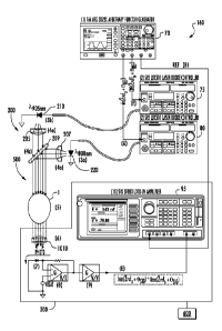
A laboratory prototype was constructed and used in several trials. A schematic
is shown
in FIG. 5.
Quadrature reference clocks
sin(2xfo + OREF) and (A)
cos(27rf0 + OREF) (F)
were generated using a Tektronix AFG 3022C Arbitrary Function Generator 70.
These two
references have arbitrary absolute phase OREF but have a relative phase of 90
to each other. The
reference signal (A) and (F) are used as modulating signals to a pair of
Stanford Research
Systems LDC 501 Laser Diode Controllers 75, 80 creating faithful reproductions
of each signal
in the optical power domain with low total harmonic distortion (THD). That is,
the optical
power output of the illumination source varies linearly with the input signal;
P
- OPT K* 'DRIVE
where Pop"' is the optical output power, 'DRIVE is the drive current through
the illumination
source, and K is a constant.
In testing, the laser diode controllers 75, 80 were used to drive the
following narrowband
illumination sources at the indicated wavelengths:
Light Emitting Diode (LED) Combinations
OSRAM SFH 4780S 680mW, 810nm
Marubeni SMBB910D-1100, 470mW, 910nm
Lasers Diode (LD) Combinations
ThorLabs L808P010 10 mW, 808nm
CA 03069323 2020-01-07
WO 2019/027814 PCT/US2018/043996
ThorLabs M5-905-0100 100mW, 905nm
Collimation lenses 205 and 207 were used when using both LEDs and LDs to
minimize
the beam dispersion and unwanted stray light. A Semrock LPD02-830RU-25 45
degree dichroic
mirror 209 with a sharp cutoff wavelength of 830 nm was used to combine the
two illumination
sources into a single beam. The combined and collimated beams were directed at
the test objects
(El 7-El 9 chicken eggs 1 of different known states (Live, Rotted, and Dead)).
The radiation transmitted through the test object was collected by a series of
three
condensing lens to increase the optical power transfer between the test object
and the detector
and to minimize light outside the +/-12 degree acceptance cone.
The detector 300 used in testing was a Vishay TEM5110X01 Silicon PIN Diode.
The
photo-current generated by the PIN diode was converted to a voltage signal
using a Texas
Instruments OPA380 high speed, transimpedance amplifier.
The output of the second gain stage (9) is represented by:
V(t) = Asin(2afo + OsiG) + Bcos(2nf0 + esici) (E)
where
OsIG = the phase of the signal at the output of the filter block,
A = the gain! attenuation of the I output of the quadrature reference
propagating to this
point,
B = the gain / attenuation of the Q output of the quadrature reference
propagating to this
point.
Magnitude (R) and phase (0) were recovered from the received signal (E) using
a 5R850
Lock-In amplifier 95.
Phase calibration was maintained by connecting the synchronization output
signal from
the TEK AFG 3022C to the SRS 5R850 External Reference Input (B). By turning
off the Q
source (905nm LD / 910nm LED), the 5R850 phase aligned with the I source
(808nm LD /
810nm LED) using a calibration feature of the instrument.
FIG. 15 plots phase angle (0) against signal power (magnitude (R)) for 120
eggs
subjected to the disclosed method at Day 18 of incubation. Each egg was
positioned on a light
sealing stand. Laser diodes (808 nm and 904 nm) were used as the light emitter
sources. The
time constant (TC) was set at 100 ms.
26
CA 03069323 2020-01-07
WO 2019/027814 PCT/US2018/043996
FIG. 16 plots phase angle (0) against signal power (magnitude (R)) for 216
eggs
subjected to the disclosed method at Day 17 and Day 18 of incubation. Each egg
was positioned
on a light sealing stand. Laser diodes (808 nm and 904 nm) were used as the
light emitter
sources. The time constant (TC) was set at 100 ms.
FIG. 19 plots phase angle (0) against signal power (magnitude (R)) for 168
eggs
subjected to the disclosed method at Day 17 and Day 18 of incubation. The eggs
were
positioned in an egg flat when subjected to the analysis. Laser diodes (808 nm
and 904 nm)
were used as the light emitter sources The time constant (TC) was set at 100
ms, with a filter
setting of " F. No attempt was made to control self-interfering light.
FIG. 20 plots phase angle (0) against signal power (magnitude (R)) for 168
eggs
subjected to the disclosed method at Day 17 and Day 18 of incubation. The eggs
were
positioned in an egg flat when subjected to the analysis. A half inch tall
section of 3/4 inch PVC
pipe was extended up to but not touching the egg flat. Laser diodes (808 nm
and 904 nm) were
used as the light emitter sources. The time constant (TC) was set at 100 ms,
with a filter setting
of "1".
FIG. 21 plots phase angle (0) against signal power (magnitude (R)) for 168
eggs
subjected to the disclosed method at Day 17 and Day 18 of incubation. The eggs
were
positioned in an egg flat when subjected to the analysis Laser diodes (808 nm
and 904 nm)
were used as the light emitter sources. The time constant (TC) set at 100 ms,
with a filter setting
of "1".
FIG. 22 plots phase angle (0) against signal power (magnitude (R)) for 168
eggs
subjected to the disclosed method at Day 17 and Day 18 of incubation. The eggs
were
positioned in an egg flat when subjected to the analysis. Laser diodes (808 nm
and 904 nm)
were used as the light emitter sources. The time constant (TC) was set at 100
ms, with a filter
setting of "8".
Many modifications and other aspects of the present disclosure set forth
herein will come
to mind to one skilled in the art to which this disclosure pertains having the
benefit of the
teachings presented in the foregoing descriptions and the associated drawings.
Therefore, it is to
be understood that the present disclosure is not to be limited to the specific
aspects disclosed and
that modifications and other aspects are intended to be included within the
scope of the appended
27
CA 03069323 2020-01-07
WO 2019/027814 PCT/US2018/043996
claims. Although specific terms are employed herein, they are used in a
generic and descriptive
sense only and not for purposes of limitation.
28