Note: Descriptions are shown in the official language in which they were submitted.
CA 03072760 2020-02-11
WO 2019/036383 PCT/US2018/046552
A SURFACE-MOUNT COMPATIBLE VCSEL ARRAY
CROSS REFERENCE TO RELATED APPLICATION
[0001] This application claims benefit of U.S. Provisional Patent Application
No.
62/545,363, filed August 14, 2017.
FIELD OF THE DISCLOSURE
[0002] The present disclosure relates to semiconductor devices, and more
particularly
to multibeam arrays of semiconductor lasers.
BACKGROUND
[0003] Vertical-cavity surface-emitting lasers (VCSELs) are a versatile type
of
semiconductor laser with unique performance advantages. They are currently
used in high-speed
data communications, optical sensing applications, such as proximity sensing,
and laser radar.
The devices are fabricated by epitaxial growth of the laser cavity, in layer
form, on the surface of
a wafer of semiconductor material, typically gallium arsenide. As a result,
they emit light in a
direction perpendicular to the wafer surface. Since it is not necessary to
cleave the
semiconductor wafer to form the laser cavity, as is required for edge-emitting
semiconductor
lasers, the devices can be readily fabricated in one and two-dimensional
arrays of VCSELs in a
single semiconductor die. The arrays of VCSELs provide a way of scaling the
output power to
higher power levels and enable individual lasers or groups of lasers in the
array to be configured
for independent power and control.
[0004] Many designs or configurations of VCSELs have been proposed and
manufactured. Most of these designs require some level of packaging to provide
protection of the
laser surfaces from the environment and to provide for connection to
conventional printed circuit
boards. A typical example is a top-emitting array of VCSELs in which an
electrical connection is
required at the top of the die. Typically, the anode (positive) contact is
close to the light emitting
junction and the cathode (negative) contact is the doped substrate of the die.
In most examples,
the anode contact is made via a wire bond to a pad on top of the die and the
cathode contact is
made via a solder bond at the bottom of the die.
CA 03072760 2020-02-11
WO 2019/036383 PCT/US2018/046552
[0005] These interconnections are not directly compatible with conventional
printed
wiring board (PWB) or printed circuit board (PCB) construction and cannot be
used directly with
high-speed, low-cost surface mount soldering processes commonly used to mass-
produce
electronic and opto-electronic systems. An electronic package is required to
make the
connections to the VCSEL die and that package has to have the appropriate
metal pads or leads
for soldering to the PCB. The package also provides protection for the VCSELs
as the
fabrication processes used often leave the sides of the epitaxial layers,
which are exposed by
etching of mesas or trenches, left unprotected, or only protected by the
polymer layers used for
planarization. The etched epitaxial layers need to be exposed for lateral
oxidation, a commonly
used process for current confinement in VCSELs. The long term exposure of
these devices to
atmospheric moisture is a known reliability problem that is usually dealt with
by using a
hermetically sealed package. Wire-bonded devices are also not easily scaled
into two-
dimensional arrays, especially if there is a need to contact many individual
lasers or groups of
lasers in the interior of the array.
[0006] Some VCSEL arrays are fabricated so light is emitted through the
substrate
wafer, either by emitting light at wavelengths for which the wafer is
transparent or through a via
in the wafer. In such architectures, the anode contact is made to the device
by bonding the anode
contact down to a conductive pad. In many designs, the cathode contact is
still made to the
semiconductor substrate surface. This allows for flip-chip bonding to be used
for making the
anode contact. Wire bonds may still be used to make the cathode contact to the
substrate surface,
which is now the top of the upside down device. A package is still needed in
most cases to
protect the device and provide pads for the wire bonds and then solder pads
for attachment to the
PCB. The need for wire bonds still severely limits the interconnect options
for a two-dimensional
array.
[0007] Such a configuration does have the advantage of the anode surface of
the laser
being in direct contact with the package substrate. This is an advantage
because the p-n junction
and mirror or DBR (Distributed Bragg Reflector) are near the anode contact and
that is where
most of the heat generated in the device is located. This makes the anode
contact the most
efficient surface for heat removal from the junction area.
[0008] The most versatile configuration of this type is shown as prior art
device 10 in
Figure 1. In the illustrated design, both the anode (laser) 14 and cathode 16
contacts are made on
2
CA 03072760 2020-02-11
WO 2019/036383 PCT/US2018/046552
the same side of the die 20. The anode contacts, 14, in this configuration
allow current to flow
through the semiconductor junctions to emit light. These contacts are
positioned very close
together for efficient use of the laser die. This allows a single flip-chip
bond step to make all the
electrical contacts. In addition, it allows for very flexible interconnection
to individual lasers or
groups of lasers in a two-dimensional array. The design uses etched mesas for
both lateral
oxidation and for electrical isolation of the anode contacts for each VCSEL.
The mesas are
completely encapsulated in a thick metal coating that provides protection from
moisture and
oxidation so that a hermetic package is not needed for reliable use. Light,
24, is emitted through
the wavelength transparent die 20. A similar design is described in detail in
U.S. Patent No.
7,949,024, which is incorporated herein by reference in its entirety.
[0009] This design still requires flip-chip bonding to a precision sub-mount
12 that
makes contact to the anode 14 and cathode 16 parts of the VCSEL array through
contact pads 22
and 18, respectively, which have a fine pitch to match the anode and cathode
contacts. Device 10
is often referred to as a precision sub-mount. The flip-chip bonding of a
precision sub-mount
requires temperatures, pressures and alignment tolerances that are not
compatible with
conventional PCB and surface-mount assemblies and soldering processes. For
this reason, the
precision sub-mount device 10 shown in Figure 1 is used with a package that
provides electrical
contacts to the VCSEL array. The device 10 requires additional contact pads to
provide contacts
to a conventional package or PCB pads.
BRIEF DESCRIPTION
[0010] The present disclosure includes a VCSEL array design (or VECSEL -
vertical-
external-cavity surface-emitting laser) that results in a VCSEL/VECSEL (herein
a "VCSEL")
array (herein a "VCSEL array") that can be directly soldered to a PCB using
conventional
surface-mount assembly and soldering techniques for mass production. In the
disclosure design,
the completed VCSEL array does not need a separate package and no precision
sub-mount and
flip-chip bonding processes are required. An additional advantage of this
design is that it allows
for on-wafer probing of the completed VCSEL arrays prior to singulation of the
die from the
wafer.
3
CA 03072760 2020-02-11
WO 2019/036383 PCT/US2018/046552
[0011] Embodiments relate to semiconductor devices, and more particularly to
multibeam arrays of semiconductor lasers for high power and high frequency
applications and
methods of making and using the same.
[0012] Embodiments may also be directed to a multibeam optoelectronic device,
referred to as a VCSEL array device, which has high power, a high frequency
response and a
variety of possible interconnections to individual lasers or groups of lasers
within the array that
can be made directly to a conventional printed circuit board using surface
mount assembly and
soldering techniques that are well known to the electronic system
manufacturing industry. The
VCSEL array device may be a monolithic array of VCSELs comprised of two or
more VCSELs
and an array or a single short-circuited mesa device. The VCSELs of the VCSEL
array may be
spaced symmetrically or asymmetrical for optimum optical or electrical
characteristics. The
VCSELs may be spaced according to a mathematical function for improved optical
properties or
electrical power transfer and speed. The VCSELs may be positioned for
electrical phase
relationships between the laser elements in the array for high fidelity of
data transmission or
optimum power transfer to the lasers.
[0013] The lasers in the array may be connected to the solder pads of the
device in
many configurations, including series and parallel electrical connections and
combinations of
those. The solder pads of the device may also be configured as desired,
including separate
electrical contacts to individual VCSELs, small common electrical contacts to
a small number of
VCSELs, or large electrical contacts to a large number of VCSELs.
[0014] The active VCSELs in the array may be contacted to an intermediate
metal
anode contact layer on a planarizing dielectric surface. The short-circuited
mesa or mesas in the
device may also be contacted to separate metallic pads in the same
intermediate metal contact
layer to form the cathode connections in the device. The anode and cathode
pads may be in the
same plane, but separated from each other by lateral gaps between the pads, as
determined by the
designer for isolation between the anode and cathode sufficient for the
voltages required for
operation.
[0015] The pattern of the anode and cathode contact pads may be configured to
allow
parallel connection of VCSELs for the anode pads and the shorted mesas for the
cathode pads.
Each anode or cathode pad may then have additional metal patterned on their
surface to provide
additional height. The metal may be plated copper or other highly conductive
metals patterned to
4
CA 03072760 2020-02-11
WO 2019/036383 PCT/US2018/046552
provide uniform contact areas to match pad metal patterns to be fabricated on
the PCB. The
additional metal may include diffusion barrier metals and be topped with a
solder alloy or
discrete solder balls may be applied to the pads. The pad patterns may be
designed for uniform
solder wetting areas to facilitate surface mount processing. The resulting
device may be
compatible with standard surface mount assembly technology and not require an
additional
package.
[0016] Each VCSEL of the VCSEL array may be encompassed by a metal heat sink
structure. The metal heat sink structure may increase the height of the mesa
and its diameter so
that heat is more efficiently removed from the VCSEL. The short-circuited
mesas may be formed
alongside the VCSELs. These devices form a short-circuit from the substrate
ground layer in the
die to cathode pad metal, completing the return to ground for the current
flowing through the
VCSELs. The metal heat sink structure may encapsulates both the VCSEL and
shorted mesas so
they are protected from moisture and other environmental factors.
[0017] The very short current paths through the VCSELs and the shorted mesas
may
minimize parasitic inductance in the device. The separation of the anode and
cathode contact
pads from the current path within the VCSEL array may minimize the parasitic
capacitance in
the device. Both act to increase power efficiency and high frequency response.
BRIEF DESCRIPTION OF THE SEVERAL VIEWS OF THE DRAWING
[0018] Fig. 1 is a side view illustrating a prior art flip-chip bonded array
with a fine
pitch.
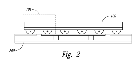
[0019] Fig. 2 is a cross-sectional side view illustrating a device in
accordance with an
embodiment.
[0020] Fig. 3 is an inverted cross section illustrating the selected part 101
of Fig. 2.
[0021] Fig. 4 illustrates the starting wafer, with epitaxially grown layers,
of the
embodiment of the device illustrated in Fig. 2.
[0022] Fig. 5 is an alternative embodiment illustrating the starting wafer
with
epitaxially grown layers shown in Fig. 4.
[0023] Fig. 6 illustrates the continued formation of an embodiment in which
initial
deposition and patterning of the contact metal to the upper DBR surface if
performed using
lithographic processes.
CA 03072760 2020-02-11
WO 2019/036383 PCT/US2018/046552
[0024] Fig. 7 illustrates the continued formation of the embodiment of Fig. 6
having
photolithographically formed mesa structures.
[0025] Fig. 8 illustrates the continued formation of the embodiment of Fig. 7
having n-
metal deposition and patterning.
[0026] Fig. 9 illustrates the continued formation of the embodiment of Fig. 8
having a
formed dielectric layers and etched vias.
[0027] Fig. 10 illustrates the continued formation of the embodiment of Fig. 9
including the patterning and deposition of metal mesa caps.
[0028] Fig. 11 illustrates the continued formation of the embodiment of Fig.
10
including the application of a planarizing layer and metal pads.
[0029] Fig. 12 illustrates the continued formation of the embodiment of Fig.
11
including the addition of metal structures over the interposer metal pads
added in Fig. 11.
[0030] Fig. 13 illustrates another embodiment to that shown in Fig. 12.
[0031] Fig. 14 illustrates a further embodiment to that shown in Fig. 12.
[0032] Fig. 15 illustrates the continued formation of the embodiment of Fig.
12
including the application of a protective resin layer on the active side and
an anti-reflective
coating and standoff structures on the back side in the embodiment.
[0033] Fig. 16 illustrates the continued formation of the embodiment of Fig.
12 having
an integrated microlens etched into the back side.
[0034] Fig. 17 illustrates an alternative embodiment of the finished wafer of
Fig. 16
where the microlens on the back side has been replaced with a via removing
substrate material
down to the epitaxial layers, over which an AR coating is applied.
[0035] Fig. 18 illustrates an alternative embodiment that includes a resin
encapsulation
on the active side with the entire substrate removed from the back side.
[0036] Fig. 19 illustrates an embodiment in which a transparent support wafer
has been
applied to the backside over the exposed surface of the epitaxial layers.
[0037] Fig. 20 illustrates an embodiment in which part or all of the upper DBR
is
replaced by a mirror formed within an addition intercavity contact layer.
[0038] Fig. 21 illustrates, in greater detail, the initial formation of the
wafer structure of
Fig. 20.
[0039] Fig. 22 illustrates the continued formation of the wafer structure of
Fig. 21.
6
CA 03072760 2020-02-11
WO 2019/036383 PCT/US2018/046552
[0040] Fig. 23 illustrates the continued formation of the wafer structure of
Fig. 22.
[0041] Fig. 24 illustrates embodiments of two exemplary layouts for VCSEL
arrays.
[0042] Fig. 25 illustrates the interposer pad metal patterns for the layouts
of Fig. 24.
[0043] Fig. 26 illustrates the contact pads or bumps for the layouts of Fig.
24.
[0044] Fig. 27 illustrates another embodiment of an exemplary layout grouping
for
VCSELs.
[0045] Fig. 28 illustrates the interpose pad metal patterns for the layouts of
Fig. 27.
[0046] Fig. 29 illustrates the contact pads or bumps for the layouts of Fig.
27.
[0047] Fig. 30 illustrates another embodiment of an exemplary layout grouping
for
VCSELs with the addition of non-conducting regions.
[0048] Fig. 31 illustrates the interposer pad metal patterns for the layouts
of Fig. 27.
[0049] Fig. 32 illustrates the posts and solder bumps for the layouts of Fig.
27.
DETAILED DESCRIPTION
[0050] Two-dimensional arrays of VCSELs are capable of providing the higher
output
power needed for many applications and are separately capable of allowing
specific elements or
groups of elements of the array to be addressed for applications such as
printing or producing
directional or variable illumination patterns. Traditional approaches to
fabricating arrays of
VCSELs have often required at least one contact pad that must be connected by
wire bonds. The
wire bonds add packaging complexity and are a source of parasitic inductance
that limits the
bandwidth of the laser array when high current pulses are used.
[0051] U. S . Patent No. 7,949,024 B2 describes the fabrication of etched
mesas that are
interconnected by flip-chip bonding to a separate submount with a metal
interconnect pattern.
The etched mesas are covered by an additional, conformal metal coating that
provides for
additional heat dissipation, environmental protection and for a larger contact
area for the later
flip-chip bonded assembly. Some of the mesas have a contact that allows
current flow through
the VCSEL device to produce light and others are electrically shorted so that
current flows
through metal that has been deposited on the outside of the mesas without
going through the
VCSEL device itself. An intra-cavity contact with a metal layer on the surface
allows for lateral
flow of current from the active (light-emitting) mesas to the shorted mesas.
This architecture
allows for both the anode and cathode contacts to be made on the same side of
the laser die and
7
CA 03072760 2020-02-11
WO 2019/036383 PCT/US2018/046552
for a single flip-chip assembly step to make all the contacts to a patterned
sub-mount that
provides the electrical contact to the mesas. This approach works very well
for minimizing
electrical parasitic inductance and capacitance or overall parasitic
impedances for the array.
However, the sub-mount is a high precision part that needs to have high
thermal conductivity.
This adds expense and the sub-mount still needs to be soldered to a PCB or put
into a
conventional sealed package that will in turn be soldered to a PCB assembly.
The additional
packaging is a source of further parasitic impedance.
[0052] An alternative approach is to build a VCSEL array that can be directly
soldered
to the PCB without an additional sub-mount or package. As described herein a
VCSEL array
design and fabrication process allows direct soldering of the VCSEL array to a
PCB using
conventional solder pad dimensions on the PCB and well-known surface-mount PCB
assembly
tools and processes, including tape and reel dispensing.
[0053] Figure 2 shows a simplified cross-section of VCSEL array device 100 in
accordance with the embodiment. The illustration shows a semiconductor device
that is an array
of surface-emitting lasers and solder bump contacts that are on a simple
geometric pattern with a
size and pitch large enough for mounting directly to printed circuit boards by
conventional
assembly processes known to those of ordinary skill in the art. The figure
depicts the VCSEL
array soldered to a simplified printed circuit board 200.
[0054] The methods described herein may be used to fabricate arrays of other
semiconductor devices, including external cavity versions of VCSELs, light
emitting diodes,
photodetectors, photomodulators and transistors. The illustration of the VCSEL
device 100 is for
illustration purposes and is not intended to limit the scope of the invention
to any specific type of
semiconductor device.
[0055] Figure 3 is an inverted more detailed illustration of the selected part
101 of
Figure 2. In the embodiment, VCSEL array device 100 may include a substrate
102 which
includes Gallium Arsenide (GaAs) or other semiconductor materials, such as
Indium Phosphide
(InP), Gallium Nitride (GaN) or Silicon (Si). The substrate may be doped as n
or p-type or may
be undoped depending on the design requirements, wavelength of operation and
placement of the
contact layer. The substrate may also be a material, such as Aluminum Oxide
(A1203) that can be
used as a substrate for the growth of semiconductor materials on the surface.
Subsequent layers
of semiconductor material may be deposited on the surface of the substrate 102
by epitaxial
8
CA 03072760 2020-02-11
WO 2019/036383 PCT/US2018/046552
growth processes, such as Molecular Beam Epitaxy (MBE) or Metal-Organo-
Chemical Vapor
Deposition (MOCVD).
[0056] In an embodiment, a starting wafer with epitaxially grown layers is
shown in
Figure 4. A lattice-matched lower Distributed Bragg Reflector (DBR) 104 may be
epitaxially
deposited on substrate 102 (as shown in Figure 5) or above the substrate 102
(as shown in Figure
4) to form the first of the layers of the active VCSEL mesas 103 and the short-
circuited or
grounded mesas 105 (shown in Figure 3). The lower DBR may be formed from
multiple layers
of alternating semiconductor alloys that have different indices of refraction.
Each layer boundary
causes a partial reflection of an optical wave with the combination of layers
acting as a high-
quality reflector at a desired wavelength of operation. While the lower DBR
104 and upper DBR
108 are composed of many layers of material, in order to simplify the
illustration, in Figure 4
they are depicted as a single material. A portion, or all, of the lower DBR
104 may also be
conductive to allow current to flow through the VCSEL device. An intracavity
contact layer 107
may be located either at the interface of the lower DBR 104 and the substrate
102 as shown in
Figure 4 or as a layer inside the lower DBR as shown in Figure 5. The
intracavity contact layer
107 may be a heavily doped semiconductor material to provide a conductive path
connecting the
mesas so as to allow lateral current flow through the device.
[0057] In an embodiment, an active region 106 may be epitaxially deposited on
the
lower DBR 104. Region 106 is again shown as a single material, but is actually
composed of
multiple layered materials to provide correct spacing for the desired
resonance wavelength and
conductivity for the current flow in the device. Region 106 may also have the
gain medium that
emits light with electrical current flow. The choice of material used for the
gain medium and the
dimensions of the other layers may serve to select a working wavelength, which
may range from
620 nm to 1600 nm for a GaAs substrate. Other material choices may extend that
wavelength
range in either or both directions.
[0058] As is understood by those skilled in the art, the emission wavelength
of the
VCSEL is determined by the choices of materials and layer thicknesses of the
materials in the
lower DBR 104 and upper DBR 108, as well as the active region 106. The gain
material may be
quantum wells, quantum dots or other semiconductor structures.
[0059] In the embodiment, upper DBR 108 may be positioned on the active region
106
and may also be electrically conductive. In some embodiments, lower DBR 104
may be p-doped
9
CA 03072760 2020-02-11
WO 2019/036383 PCT/US2018/046552
and upper DBR 108 maybe n-doped, but some embodiments may reverse that order.
The upper
DBR 108 may also be partly or completely composed of a non-conducting
dielectric layer stack
that is not epitaxially grown semiconductor material, but rather thin-film
layers deposited by
evaporation or sputtering with electrical contact made to an intracavity
contact layer within or
below the upper DBR. As depicted in Figures 4 and 5, all of these layers are
typically in a single
epitaxial structure grown on the substrate 102 which constitutes a starting
point for subsequent
processing steps. In Figure 4, the lower DBR 104 is positioned above the
intracavity contact
layer 107 and in Figure 5, the lower DBR 104 is positioned below the
intracavity contact layer
107, in each case with the active region 106 between the lower DBR and upper
DBR (forming
the distributed DBR).
[0060] The upper DBR 108 may terminate in a heavily-doped contact layer to
facilitate
an ohmic contact to a metal contact layer, 120. Figure 6 shows the initial
deposition and
patterning of the contact metal 120 to the upper DBR 108 surface, and the
patterned dielectric
layer 114 on top of the metal contact layer 120 using lithographic processes
well known to those
skilled in the art. If an ion-implanted confinement is part of the final
structure, that implantation
step may be performed prior to the contact. In that case, a prior metal
deposition and patterning
step may be performed to provide alignment features for the ion-implantation
and subsequent
steps.
[0061] The next step is illustrated in Figure 7 and involves creation of the
mesa
structures 103 and 105. A robust photolithographically defined mask is needed
for etching of the
mesas into the epitaxial layer structure. This may use the patterned
dielectric layer 114 (shown in
Figure 6), such as SiN or a combination of the dielectric material with a
photoresist layer. The
contact metal 120 patterned (as shown in Figure 6) is also protected by this
layer. The exposed
sides of the mesas 103 and 105 shown in Figure 7 allow for lateral oxidation
of one or more high
aluminum content AlGaAs layers 110 as one approach to charge carrier and light
confinement in
the mesa. Note that the contact metal on top of the mesas may still be covered
by the dielectric
etch mask at this stage. Photoresist layers that may be part of the etch mask
can be removed at
this point.
[0062] The mesa etch may be a controlled etch process using dry (plasma) or
wet etch
processes that stops at the intracavity contact layer 107, that is in the
lower (n-type) DBR 104, or
CA 03072760 2020-02-11
WO 2019/036383 PCT/US2018/046552
just under the DBR at the interface of the lower DBR 104 and the substrate
102. Selective etch
stop layers may be part of the intracavity contact layer to produce a more
uniform etch depth.
[0063] Another contact metal layer 122, as shown in Figure 8, may be deposited
and
patterned at this point on the exposed surface of the intracavity contact
layer 107. This may
typically be a metal layer structure optimized for making an ohmic contact to
the contact layer.
This may also be the point at which thermal annealing may be used to
interdiffuse the contact
metal into the semiconductor material surface. The active light-emitting mesas
are mesas 103
and the shorted mesas are mesas 105.
[0064] As shown in Figure 9, a second dielectric layer 116 may then be
deposited on
the wafer surface that covers all the features. This layer may allow for
isolation of the shorted
mesas from the active, light-emitting mesas. Another photolithography step may
be used to
define the regions of the dielectric layer 116 that need to be exposed by
etching to allow
electrical contact to the active mesas 103 where current will flow through the
mesa structure to
cause the laser to emit light. This step is also shown in Figure 9. Note that
the dielectric layer
116 may only be removed from selected areas of the n-contact metal 122.
[0065] The next step is illustrated in Figure 10, where a thick metal cap 124
is shown
formed over the mesas 124 to protect the mesas, to make an electrical
connection to the n-contact
metal for the shorted mesas, to act as the p-contact for the active mesas, and
to provide additional
heat transfer. If this metal cap 124 may be deposited by electroplating, a
thin "seed" metal layer
123 may be deposited first across the entire wafer to provide electrical
continuity. A thick
photoresist mask may then be applied and photolithographically patterned for a
thick metal
deposition. Removal of the photoresist may then be followed by a selective
etch of the exposed
seed metal layer.
[0066] As noted, the thick metal cap 124 on the mesas may be in electrical
contact to
the n-contact metal on the active laser mesas 103 while being separated from
the mesa surface
and the p-contact metal on the shorted mesas 105 by the remaining dielectric
layer 116. The
thick metal cap 124 on the shorted mesas 105 overlap exposed area of the n-
contact metal. This
allows the return current from the VCSEL mesas to flow through the n-contact
metal where it is
in contact with the intracavity contact layer in or near the lower DBR 108 to
the metal cap on the
shorted mesas. Then the current flow does not go through the shorted mesa, but
flows through
the thick metal heat sink cap, 124. The resulting structure is shown is Figure
10.
11
CA 03072760 2020-02-11
WO 2019/036383 PCT/US2018/046552
[0067] The metal mesa caps 124 may necessarily be on the same pitch as the
mesas and
may only be several microns larger than the original mesas depending on the
thickness of the
additional metal. An efficient VCSEL array may have the mesas located on a
fine pitch and the
mesas may usually be limited in size. The mesa caps 124 do not provide a
compatible interface
to solder pads on conventional PCBs.
[0068] The next steps are shown in Figure 11. A planarizing layer of
nonconductive
material 128 may be applied to the wafer in order to fill all the gaps between
the mesas and
provide a surface level with the tops of the metal caps 124 on the mesas. This
may typically be
done with spin deposition of a polymer like polyimide or bisbenzocyclobutene
(BCB) or with a
spin-on glass (sol-gel) formulation. Careful control of the parameters allows
for the applied layer
to match the height of the mesas. Additional solvent removal or mechanical
polishing may be
used to exactly match the height of the mesas. Other deposition processes may
also be used to
create the planar surface.
[0069] The two types of mesa, 103 and 105, may be slightly different heights,
due to
the removal of layers 114 and 116 from the active mesas 103. The height
difference may be
small enough that the planarization step can provide a sufficiently uniform
contact pad surface
130 for soldering purposes.
[0070] Once the planarizing material is hardened or cured, a photolithographic
pattern
process may be completed to pattern interposer metal pads 130 that contact the
metal caps. These
pads can be much larger than the mesas and separately provide electrical
contact to groups of
active mesas or individual active mesas to form the anode pads and to groups
of shorted mesas or
individual shorted mesas to form cathode pads. The pad shapes and spacing may
provide great
flexibility in how the mesas are interconnected. The pad metal may be gold or
a layered
structure optimized for heat dissipation and high electrical conductivity. An
example is a thin
gold layer to contact the tops of the metal caps (also gold in this example)
and then a thick layer
of plated copper to provide high lateral conductivity and heat transfer. The
effect of the pads 130
is to provide an interposer layer to allow the final solder bumps to be on a
significantly different
pitch and size than the mesas. The additional surface area and thermal mass
can greatly increase
the thermal dissipation of the VCSEL array compared to the metal heatsink caps
124 by
themselves.
12
CA 03072760 2020-02-11
WO 2019/036383 PCT/US2018/046552
[0071] The pattern of the pad metal 130 may not be the best layout for
compatibility
with surface mount processes and may therefore be somewhat arbitrary in size
and shape, in
order to accommodate the patterns of mesas that need to be connected together,
due to the
functional, optical and electrical requirements for the VCSEL array. In order
to provide a
uniform array of contact pads ideally configured for soldering to PCB solder
pads with
automated assembly and solder reflow methods an additional metal structure of
metal pads,
posts, pillars or bumps 132 may be fabricated on the interposer pads 130. In
Figure 12, the metal
pads, posts, pillars or bumps 132 are depicted as much thicker and larger than
the VCSEL mesas,
but may be smaller and may be patterned more densely, depending on the
manufacturing
processes available. The key point is that they provide for good mechanical
and metallurgical
bonding to the PCB solder pads and can be located on the underlying pad metal
130 so that they
match up to the PCB solder pad dimensions and spacing. This allows separate
optimization of
the VCSEL array dimensions and spacing from the electrical contact functions
of the device.
[0072] Figure 12 illustrates the resulting metal structures according to a
first
embodiment, a combination of posts 132 and solder metal layer 136 that may
provide the actual
solder bonding surfaces for the VCSEL array. Copper electroplating of the
posts 132 provides a
thick structure that can carry large amounts of current with very low loss and
low parasitic
inductance. The copper posts may be terminated with a metal layer structure
optimized for good
adhesion and compatibility with common solders used for surface mount
assembly. An example
is a layer of gold on the surface of the copper posts 132 with a diffusion
barrier of nickel
followed by a thin corrosion barrier of gold. There are many variations of
commonly used under
bump metallization (UBM) known to those skilled in the art. The fabrication of
the copper posts
may require another application of a continuous thin metal seed layer, a thick
photoresist layer
photolithographically patterned to create the desired size and pitch of copper
posts. After
electroplating, and possibly replanarizing by chemo-mechanical polishing
methods, the
photoresist may be stripped, and any seed metal layer stripped away. Figure 12
shows an
optional additional solder metal layer 136 on the top of the metal posts. This
layer 136 may be
deposited electrochemically after the other metals in the post structure, or
may be applied
afterwards by other deposition methods, including evaporation, electroplating,
jet deposition or
mechanical application of discrete solder balls.
13
CA 03072760 2020-02-11
WO 2019/036383 PCT/US2018/046552
[0073] A second embodiment is shown in Figure 13 in which an additional
planarization layer 134 of polymer or other dielectric material is applied
after the completion of
the interposer metal pads 130. This layer can also be patterned and used to
define the shapes of
the metal posts 132, but may be left in place to insulate the interposer pads
from the deposition
of the solder 136 and from the soldering reflow process itself. The additional
planarization
dielectric 134 can also be left higher than the metal posts 132 to facilitate
the assembly of
discrete solder balls onto the metal post 132 surfaces.
[0074] Another embodiment, shown in Figure 14, does not use the plated copper
posts,
but uses a solder wetting barrier 138 directly on the anode and cathode pad
metal 130 so that
specific areas of the pad can have solder deposited or can be bonded with
solder paste applied to
the PCB. The solder wetting barriers can be dielectric material or metals
known to those skilled
in the art to not allow wetting by solders used for attachment to the PCB.
[0075] As embodiments of the VCSEL array design disclosed herein is for
devices that
will emit light through the surface of the substrate 102, additional process
steps may typically be
needed for the other side of the wafer. At this point the side of the wafer
with the mesas (the
"active side") may need to be protected while processing is performed on the
other side (the
"back side") of the substrate wafer. One approach illustrated in Figure 15 may
be to encapsulate
the exposed metal posts and the gaps between the posts in a removable resin
140, such as
photoresist or a wax or resin that can be applied uniformly and easily removed
by solvents. A
mechanical "handle" wafer (not shown), such as a silicon or quartz wafer may
then be bonded to
the surface of the resin 140 for additional mechanical support during the
processing of the back
side of the wafer. Figure 15 shows the device structure with the resin
encapsulation 140 in place
and the substrate thinned by mechanical and chemo-mechanical means. The back
side of the
substrate is also polished for low scattering loss. An anti-reflection (AR)
coating 142 can also be
applied to reduce Fresnel reflection losses from the substrate surface. The AR
coating can also be
photolithographically patterned by an etch or liftoff process to provide
labeling information as
the light emission surface will be the surface visible after assembly.
[0076] A standoff structure in metal or a durable heat-resistant polymer
material 144
can be applied to the back side of the wafer to provide protection of the AR
coated surfaces
during handling and assembly. The completed device, after removal of the any
handle wafer and
the encapsulating resin 140 is as shown in Figure 16. The resulting finished
wafer can then be
14
CA 03072760 2020-02-11
WO 2019/036383 PCT/US2018/046552
diced, and each individual die can be a completely packaged part with solder
pads large enough
in size and pitch to be soldered directly to a PCB by standard assembly
techniques.
[0077] The backside or emission side of the wafer can also be used to
fabricate optical
structures, including microlenses, for control of beam direction and beam
properties of the lasers.
Figure 16 further illustrates an example of a microlens 146 etched into the
substrate for this
purpose. This step can be done right after the wafer thinning step so that an
AR coating 142 can
then be applied to the lens surface. There are numerous processes for
fabricating microlenses on
the surface of the array that are known to those skilled in the art, including
reflow of polymers,
transfer etching of a resist profile formed by grayscale lithography or reflow
of a resist.
Diffractive structures including gratings, Fresnel lenses, kinoforms and
computer-generated
phase relief holograms may also be fabricated on the back side of the wafer
for control and
manipulation of the output beams of the VCSELs.
[0078] In some cases, the wavelength of the VCSELs will be designed to be
short
enough that the semiconductor substrate 102 is absorbing at the operating
wavelength, resulting
in unacceptable light emission losses even when the substrate is thinned.
Figure 17 shows a
variation of the VCSEL array of Fig. 16 in which the processing on the back
(or emission) side
of the wafer includes etching of vias 148, in place of microlens 146, so as to
remove all substrate
material in the beam path. This process may be enabled by including a suitable
selective etch
stop layer, known to those skilled in the art, in the epitaxial growth
structure 149 at the interface
of the lower DBR 104 and the substrate 102. The via may then be patterned in
photoresist on the
backside of the wafer and a selective wet or dry etch may be used that will
stop at the layer that
greatly slows the etch process. An AR coating 142 may be applied to the
exposed epitaxial layers
149 as well as the remaining substrate.
[0079] In other cases, it may be desirable to remove the substrate entirely
from the
wafer while it is still attached to a handle wafer, as discussed in reference
to Figure 15. When
that is done, the extremely thin epitaxial layers 149 that make up the VCSEL
array and the added
metal and planarization layers would be all that was left, as shown in Figure
18. A new support
wafer 150 that is transparent to the laser wavelength may then be bonded to
the exposed surface
149 as shown in Figure 19. The exposed semiconductor surface 149 or the
surface of the
transparent wafer can have an antireflection matching coating to minimize
reflections between
the two material that are likely to have a large index mismatch and high
reflection losses. The
CA 03072760 2020-02-11
WO 2019/036383 PCT/US2018/046552
emission side of the transparent wafer 150 can also have an AR coating 142, as
well as
microlenses, other micro-optical devices, and protective standoff frames
similar to those
described above.
[0080] The transparent wafer 150 may have a high reflectivity coating on the
surface so
that it forms an extended cavity of the lasers for larger mode volume devices
with higher power
and improved brightness. This type of device is commonly referred to as a
VECSEL. The
transparent wafer 150 may also be a doped glass or crystalline laser gain
medium with
appropriate coating to make a diode-pumped solid-state laser array where the
VCSEL laser
elements are the pump lasers.
[0081] Another alternative embodiment is shown in Figure 20. In this
embodiment,
device 160 includes a second intracavity contact layer 162 that may be grown
in the upper DBR
structure. The upper DBR structure may be many fewer layers than in other
embodiments or
omitted completely, depending on the detailed laser design and replaced by a
spacer layer and a
doped contact layer configured to support the growth of a sequence of
dielectric layers on top.
The second intracavity contact layer 162 may be a heavily doped semiconductor
layer that
facilitates high lateral conductivity and provides a good ohmic metallic
contact. Instead of a full
upper DBR fabricated of epitaxial semiconductor alloys, as used in other
embodiments, a
separate mirror 165 may be deposited after the formation of a metal contact,
such as an annular
ohmic contact 170, on the upper intracavity contact layer 162. The annular
ohmic contact 170
(shown in Figure 22) has an opening large enough for the planned laser
aperture or a resonant
LED if used for that purpose. The mirror 165 may be a dielectric stack of
contrasting index of
refraction materials commonly used by those skilled in the art of making high
reflectivity, low
loss laser mirrors. The dielectric mirror 165 may be designed for phase
matching to the partial
upper DBR layers 168 if they are used. The mirror 165 does not conduct
current. The upper
intracavity contact layer 162 conducts the current from the annular ohmic
contact 170. One
advantage of this type of device is that the semiconductor-based DBR layers
can be inefficient
for longer wavelength lasers designs. This design approach also reduces ohmic
losses as the
current does not have to go through the full thickness of semiconductor DBR
layers.
[0082] Figure 21 shows in greater detail the epitaxial wafer structure of
Figure 20
having the second intracavity contact layer 162 as well as the lower
intracavity contact layer 107
and a reduced thickness top DBR layer structure 168. Figure 22 shows the same
device structure
16
CA 03072760 2020-02-11
WO 2019/036383 PCT/US2018/046552
after deposition and patterning of the annular metal layer 170, which makes an
ohmic contact to
the top intracavity contact layer 162. As shown in Figure 23, the laser mesa
103 in this case has
the contact metal 170 patterned with an opening in the center of the mesa 103.
The mirror layers
165 are deposited over the ohmic contact 170 so that the opening is filled
with the dielectric
layers to create a high reflectivity laser cavity. The size of the final
mirror, which may be a
hybrid mirror combining the dielectric mirror layers with a partial upper DBR,
needs to be large
enough relative to the laser aperture formed by the oxidation of the high
aluminum content layers
110 (shown in Figure 7) or by ion implant. In Figure 23 the laser mesa 103 and
the shorted or
grounded mesa 105 are formed as described earlier. At this stage, fabrication
of the completed
device may be substantially the same as described above, provided care is
taken to protect the
mirror layers 165 during the process steps.
[0083] In accordance with an embodiment, Figures 24-26 illustrate top views of
two
exemplary layouts for a VCSEL array following the processes illustrated in
Figures 10-12.
Active laser mesas 103 are grouped in the middle area, surrounded by n-contact
metal 122,
which is ringed by shorted mesas 105. Figure 24 illustrates the sequence of
capped mesas 124
formed by completion of the process illustrated in Figure 10. Figure 25
illustrates the interposer
pad metal 130 added as a result of the process illustrated in Figure 11.
Figure 26 illustrates the
solder bumps 136 added to the tops of the metal posts 132 in Figure 12. As
illustrated in Figure
25, for both layouts, interposer pad metal pattern 130a connects all of the
active laser mesas 103
in parallel while the other interposer pad metal pattern 130b connects all the
shorted mesas 105
together. In this embodiment, the metal posts 132 for pad metal pattern 130a
are the anode
contacts of the device and the metal posts 132 for pad metal pattern 130b are
the cathode
contacts of the device. Note: as illustrated in the left layout of Figure 26,
the metal posts 132 do
not have to be cylindrical structures as in the example in Figures 12-20. The
shape of the metal
contact posts may be designed for optimum solder contact area for ease of
assembly, high
thermal conduction into the PCB metal, strong mechanical solder bond strength
and high
conductivity and low inductance.
[0084] Figure 27 illustrates another exemplary layout for a VCSEL array. As
shown in
Figure 27, the capped mesas 124 are configured similarly to the configurations
of Figure 24, but
the active laser mesas 103 may be separated into two groups by a gap 175.
Likewise, the
interposer pad metal 130a may be separated into two areas for the VCSELs
(active mesas) 103,
17
CA 03072760 2020-02-11
WO 2019/036383 PCT/US2018/046552
as shown in Figure 28. In this case the shorted mesas 105 are still all
contacted in parallel for a
low impedance current return path and because the VCSELs all share common
ground
connection through the intracavity contact layer in the lower DBR 108. The
metal contact posts
132 illustrated in Figure 29 are also now separately connected into contact
pads for soldering the
device to a PCB, each connecting to a group of VCSELs (active mesas), 103.
[0085] Separation of the active mesas (VCSELs) in this manner makes it
possible to
independently turn on and off the groups of VCSELs and allows for the groups
of VCSELs to be
independently modulated, such as by connecting the separate contacts through
separate pads on
the PCB. This is a very flexible embodiment for configuring a VCSEL array for
specific
applications through the final fabrication steps. The layout of the mesas 103
and 105 can be on a
fixed pitch that is optimized for efficient current spreading through the
array and for balanced
heat load across the array and the final electrical configuration decided by
the design of the
interposer pad metal 130 pattern and the metal contact post 132 pattern.
[0086] Flexibility in the design of the contact pad layout 130 is limited by
the fact that
in the fabrication sequence depicted thus far the VCSELs are all connected in
common through
the intracavity contact layer. This contact layer, however, can be altered in
the fabrication
sequence by an additional trench etch or isolation implant so that groups of
VCSELs (active
mesas) 103 are isolated from each other. In such an embodiment, it is
desirable to have an
undoped semiconductor substrate 102 so that only the intracavity contact layer
and any doped
layers in the lower DBR 104 need to be made nonconducting in regions to
separate the groups of
VCSELs electrically. This may be accomplished by ion implantation into areas
of the conductive
layers so that the disordering of the implant renders those area
nonconducting. Another approach
is to do a second etch step after the mesa etch to physically isolate the
regions from each other by
etching through the intracavity contact layer and a remaining doped lower DBR
layers.
[0087] Figure 30 shows a top view of a VCSEL array in which an additional ion
implant is used after the mesa etch step to render non-conducting regions 138
of the intracavity
contact layer, and to make the lower DBR 104 nonconducting. The groups of
VCSEL mesas and
shorted mesas shown are now electrically isolated from each other. As shown in
Figure 31, the
interposer pad metal 140a and 140b are also electrically separated. Figure 32
shows the metal
contact post and solder areas 142a, 142b, 142c and 142d that may make contact
to separate PCB
solder pads so that the cathode contacts of one part, for example anode
contact 142a, can be
18
CA 03072760 2020-02-11
WO 2019/036383 PCT/US2018/046552
connected to the current supply through the PCB board. The cathode contacts
142b then are
connected to the anode contacts 142c of the second group. The current flow
then returns to
ground through cathode contacts 142d. The result is to connect the two groups
of lasers in series
through the PCB connections.
[0088] It is possible to connect the cathode contacts 142b to the anode
contacts 142c on
the die itself, so that only contacts 142a and 142d need to be connected to
the power and ground
contacts on the PCB and the two regions of the die are connected in series.
However, in the
preferred embodiment as shown in Figure 32, the contact pads 142a, and 142b
are isolated from
contact pads 142c and 142d by the non-conducting region 138 so that the PCB
designer can
connect the two laser regions (142a and 142c) in parallel or in series as
preferred by the designer.
[0089] The embodiments of the present disclosure, while illustrated and
described in
terms of various embodiments, are not limited to the particular descriptions
contained in the
specification. Different materials and different combinations of elements may
be used in a
manner consistent with the present disclosure to develop additional
embodiments. Additional
alternative or equivalent components and elements may also be readily used to
practice the
present disclosure.
19