Note: Descriptions are shown in the official language in which they were submitted.
CA 03073008 2020-02-13
WO 2018/033862 PCT/IB2017/054972
1
METHOD TO CREATE THIN FUNCTIONAL COATINGS ON LIGHT ALLOYS
BACKGROUND
[0001] Aluminium and its alloys are a widely used material for automotive,
structural and aerospace applications, however without suitable functional
coatings many alloys suffer from environmental degradation due to corrosion. A
number of processes have been developed to protect aluminium surfaces
including anodizing, plating and chemical films. However, to effectively
protect the
aluminium surface either a thick plated or anodized film is required.
Alternatively,
thin films of environmentally hazardous materials such as cadmium or
hexavalent
chromium are required.
[0002] Anodizing is one well recognized method to protect aluminium and
other
light metal surfaces. Different applications of an anodized surface may
utilize
either a thick film, where high protection is required, or a thin film for
more
decorative applications. In thick film or hard anodizing an oxide surface
between
25 and 150 microns thick is developed. This surface is typically sealed in a
process that may include dying. Other protective coatings may be subsequently
applied to this surface. Two patents U.S. 4,431,707 and U.S. 4,624,752
describe
methods to further treat hard anodized surfaces so that they may be plated.
Both
of these methods include a chemical etch phase to create a layer to which an
electrically conductive surface may be applied and plated layers
electrodeposited
on this surface.
[0003] Thin film anodized surfaces are typically between 0.5 and 25
microns.
As with hard anodizing these surfaces are normally sealed to provide
environmental protection. An advantage of thin anodized surfaces is that
sufficient
electrical conductivity remains between the substrate through the anodizing
pores
that it is possible to directly electrodeposit functional films on the
anodized surface.
Patents U.S. 3,915,811 and U.S. 3,943,039 describe methods to further treat
anodized films and electro deposit, especially nickel coatings, on such films.
These patents specify different baths and processes for the anodizing while
suggesting a variety of approaches to electro-deposition to provide a
functional
surface. Both these patents are directed at a subset of aluminium alloys of
particular importance to the automotive industry for car bumpers and typically
CA 03073008 2020-02-13
WO 2018/033862 PCT/IB2017/054972
2
involve electro-depositing one or more thick layers to achieve the corrosion
protection and decorative aspects of these applications. More specifically
these
patents do not teach the approach disclosed in this application to ensure
complete
filling of the anodizing pores and allow thin film electro-deposited surfaces
to
achieve good corrosion protection and other functional properties.
[0004] Electro-deposition on aluminium is also well known and the process
typically involves applying a very thin zinc layer to the surface using a
zincate
process followed by applying one or more plated coatings on this surface. The
zincate process is inherently problematic and essential to achieve a good
electrodeposited coating, thus double and triple zincate steps are often
required to
achieve acceptable results. In many instances, the first plated layer is a
thick (40-
50 microns) electro-less Ni-P coating or semi-bright electrolytic nickel to
provide
corrosion protection. This first layer is followed by a functional or
decorative
surface layer which may be a bright nickel. In one application, the surface
coating
is electro-deposited Zn-Ni. The Ni-P/Zn-Ni coating system has been developed
to
replace environmentally dangerous chromate passivated cadmium for electrical
connector shells. However, the process is both expensive in time and materials
and not as effective as the coating it is designed to replace.
[0005] Thin anodized films are also used as a template to produce nano-
wires
for sensors, such as that described in US 2009/0242416. While this patent
teaches plating in the pores of an anodized surface it does not teach
controlling
the current to ensure complete filling of the nano-pores and achieving an
interlock
between the nano-wire and the pore. Nor does it teach increasing the current
when the pores are filed to ensure complete coverage of the anodized film.
[0006] Consequently, there is a need in the art for a method to coat
aluminium
and other light metal surfaces with thin plated coatings that provides
protection
from corrosion and other functional attributes.
SUMMARY
[0007] According to aspects illustrated herein, there is provided a method
for
producing a thin film coating. One disclosed feature of the embodiments is a
method comprising pre-treating a substrate, placing the substrate in a bath
comprising at least phosphoric acid and sulphuric acid to produce a thin
anodized
CA 03073008 2020-02-13
WO 2018/033862 PCT/IB2017/054972
3
layer, rinsing the thin anodized layer in a solution, plating a surface of the
thin
anodized layer in an electro deposition bath following a plating current
profile for a
predetermined period, and increasing the plating current to the recommended
bath
plating current to produce the thin film coating having a desired initial
coating
thickness.
BRIEF DESCRIPTION OF THE DRAWINGS
[0008] FIG. 1 is a scanning electronic microscope (SEM) image of an
anodized
surface;
[0009] FIG. 2 is a SEM of an anodizing flaw;
[0010] FIG. 3 is a SEM of a filled anodized layer cross-section;
[0011] FIG. 4 is an image of a unique morphology;
[0012] FIG. 5 is an image of example effects of hemispherical surface
morphology;
[0013] FIG. 6 is an image of a cross-section of a hybrid SB/bright Ni
coating;
[0014] FIG. 7 is an image of an adhesion test of a hybrid SB/bright Ni
coating;
[0015] FIG. 8 is an image of pre and post copper accelerated acetic acid
salt
spray (CASS) testing images;
[0016] FIG. 9 is an image of a duplex hybrid coating with Zn-Ni surface;
[0017] FIG. 10 is an image of adhesion test results for duplex hybrid
coating;
[0018] FIG. 11 is an image of pre and post CASS test results for duplex
hybrid
Zn-Ni coating;
[0019] FIG. 12 is an image of a surface morphology of hybrid black nickel
coating;
[0020] FIG. 13 is an image of UV-Vis-infrared light absorption properties;
[0021] FIG. 14 is an image of wear resistance under 1N load;
[0022] FIG. 15 is an image of a surface morphology of the hybrid black
nickel
coating;
[0023] FIG. 16 is an image of comparative wear tracks of a hybrid coating
and
traditional coating;
[0024] FIG. 17 is an image of example thicknesses of various layers; and
[0025] FIG. 18 is a flow chart of an example method for producing a thin
film
coating.
CA 03073008 2020-02-13
WO 2018/033862 PCT/IB2017/054972
4
DETAILED DESCRIPTION
[0026] Examples described herein provide an improved process to develop a
thin plated coating on an aluminium or light metal alloy. The process
incorporates
one of more of the following steps: degreasing an alloy substrate; electro
polishing
the substrate; activating the surface; anodizing a film of between 1 and 10
microns
on the substrate in an anodizing baths comprising substantially phosphoric
acid;
optionally activating the anodized surface in a solution containing
hydrofluoric acid
to completely dissolve the anodized surface end-caps; electro-depositing a
first
plated layer of between 1 and 20 microns (including the anodizing film)
adopting a
voltage profile for the electro-deposition to ensure the anodizing pores are
completely filled and sealed and develop a surface onto which other coatings
may
be deposited; optionally a sealing phase using nickel acetate bath may follow
the
first plating step to seal any anodizing pores not completely filed by the
first plating
step; and optionally depositing a second, or a multi-layer, functional coating
of
between 0 and 20 microns on the first layer. The total average thickness of
the
hybrid coating may be around 2 to 40 microns.
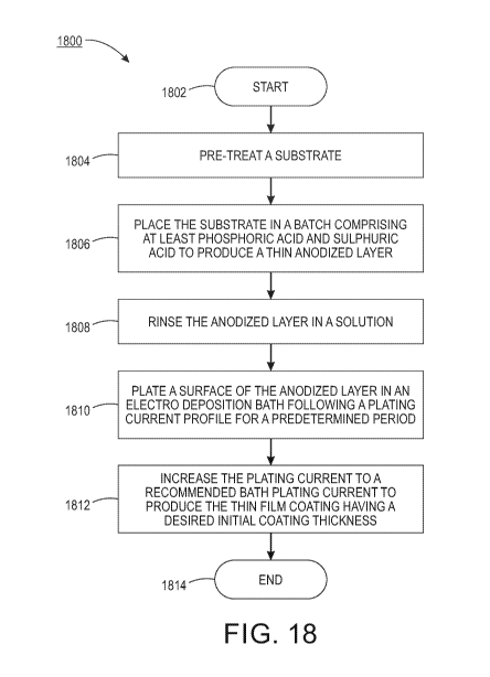
[0027] FIG. 18 illustrates an example method 1800 for producing a thin film
coating. In one embodiment, the method 1800 may be performed by various
equipment or tools in a processing facility under the control of a processor
or
controller.
[0028] At block 1802, the method 1800 begins. At block 1804, the method
1800
may pre-treat a substrate. In one embodiment, the substrate may be aluminium,
titanium, or magnesium.
[0029] The pre-treatment may include degreasing the substrate in an
alkaline
bath, roughening the substrate in a solution of polyethelene glycol, sulphuric
acid
and hydrofluoric acid, or other similar solution, and etching the substrate in
a nitric
acid solution. An example of solution may be a commercial aluminum surface
pretreatment called Probright AL. The solution to roughen the substrate may
clean the substrate surfaces as it etches.
[0030] One example of the pre-treatment may include the substrate first
being
treated by degreasing in a commercial solution such as Activax from MacDermid.
The degreasing step is followed by rinsing and electro polishing in a bath
CA 03073008 2020-02-13
WO 2018/033862 PCT/IB2017/054972
containing H3PO4, HF, H2SO4 and Glycerol in a volume ratio selected from the
following ranges 70-85:2-4:6-9:5-20. The rinsing of the substrate prior to
anodizing has the effect of eliminating impurities on the surface, which may
cause
imperfections in a thin anodized layer. Such impurities include insoluble
alloying
elements in the substrate. The electro polishing bath is held at a temperature
of
between 70 and 80 Celsius ( C) at a voltage (V) of approximately 12V. The
electro
polishing step provides a uniform surface of the substrate with minimal
alloying
elements of the surface which contributes to achieving a uniform anodized
layer.
The electro-polished substrate is then rinsed in de-ionized (DI) water prior
to the
activation and anodizing step.
[0031] In one embodiment, the substrate may be optionally activated prior
to
anodizing. The activation step may provide some benefits on certain alloys.
One
example of the activation step may include activating the surface in a bath
comprising HNO3 normally 40% by volume, but between 20 and 50 V% can be
effective, and between 1 and 10 milliliters per liter (mL/L) of HF. The bath
is
maintained at a temperature between 20 C-25 C with the substrate being
immersed and agitated about once per second for between 20 and 40 seconds.
[0032] Another example of the activation step may include a short anodizing
step for 1 minute or less, also referred to as "patterning." The patterning
may
improve the quality of the anodizing film. One example includes the removal of
the
developed anodizing layer in a sodium hydroxide bath, rinsing, and then
anodizing
again following the anodizing process described herein.
[0033] At block 1806, the method 1800 places the substrate in a bath
comprising at least phosphoric acid and sulphuric acid to produce a thin
anodized
layer. In one embodiment, the electrical parameters and bath composition of
the
anodizing step are carefully controlled to ensure that the anodized surface
contains a uniform high-density distribution of thin walled pores between 50
and
70 nanometers (nm) in diameter, as shown in FIG. 1. The anodizing bath which
contains principally phosphoric acid with small amounts of both sulphuric and
oxalic acids is operated at room temperature (20 C-25 C). A bath composition
is
selected from the range H3PO4 280-600 grams per liter (g/L), H2504 1-15g/L and
HOOCCOOH 1-10g/L. Constant voltage anodizing at a voltage of between 30V
and 60V and a maximum current density of 2 amperes per square decimeter
CA 03073008 2020-02-13
WO 2018/033862 PCT/IB2017/054972
6
(A/dm2) provides an optimum pore distribution and density. The thickness of
the
anodized film in the present disclosure is between 1 and 10 microns; however,
the
thickness may also be between 1 and 5 microns. In one embodiment, the
thickness may be between 1 and 2 microns. Anodizing for 10 minutes at the
above
described conditions results in an anodized film of about 2.5 microns. The
thin
anodized layer becomes a keying layer for a hybrid coating system allowing
subsequently deposited layers to securely interlock with this layer to provide
superior adhesion over traditional plated solutions.
[0034] A problem to be managed, during the anodizing step, when anodizing
thin films, is the incomplete dissolution of some alloying element, such as
silicon
and iron, from the substrate. The electro polishing and activation steps,
prior to
anodizing, reduce but do not eliminate the presence of these elements from the
surface. The presence of these elements may result in anodizing flaws as shown
in the SEM image in FIG. 2. These flaws may create imperfections in the first
electrodeposited layer where the first electrodeposited layer either does not
completely cover, or does not completely interlock, with the anodized layer
resulting in both low adhesion and potential corrosion pathways. The selection
of
low temperature and low constant voltage anodizing minimizes the creation of
such flaws. The optional sealing step may eliminate potential corrosion
pathways.
[0035] At block 1808, the method 1800 rinses the anodized layer in a
solution.
In one embodiment, the rinsing may be used to completely dissolve the
anodizing
end-caps at the bottom of the pores. The solution may be a bath comprising
between 0.5-5 mL/L HF. The anodized substrate to be processed is immersed in
the rinse bath for approximately 30 seconds while being agitated about once
per
second.
[0036] At block 1810, the method 1800 plates a surface of the anodized
layer in
an electro deposition bath following a plating current profile for a
predetermined
period. For example, a first electrodeposited coating is applied to the
anodizing
film from a bath selected from a range of possible baths. The electrical
parameters pertaining to the first electrodeposited coating are controlled
where a
first plating current is applied for a first plating period comprising a first
plating
stage and a second plating current is applied for a second plating period
comprising a second plating stage. The first electro-deposited layer forms an
CA 03073008 2020-02-13
WO 2018/033862 PCT/IB2017/054972
7
interlock layer completely filling the pores in the anodised layer securely
locking
the first electroplated layer to the anodised surface.
[0037] The first plating stage which proceeds for the first plating period
during
which the first plating current, or current profile, is set at a percentage of
the
nominal plating current for a chosen bath composition. The nominal plating may
be defined by the Technical Data Sheet (TDS) provided by a formulator for a
particular plating bath. For example, the plating current for the semi-bright
nickel
referred to herein may be between 2 and 4 A/dm2. In one embodiment, the
nominal plating current may be 3 A/dm2 for the bath described herein. The
first
plating current, or current profile, is selected to be between 5% and 50% of
the
nominal plating current for a chosen bath composition and the first plating
period is
dependent on the thickness of the anodized film, but sufficient to completely
fill the
anodized pores with an electro deposited coating. The amount of time that is
sufficient may be defined by the function below. In one example, for a semi-
bright
nickel bath and a plating current of 16% of the nominal plating current and an
anodizing layer of 2 microns, 18 minutes may provide a sufficient amount of
time.
The plating rate for this reduced current has been shown to be between 0.05
and
0.5 times that for the bath under normal operating conditions. Thus, the first
plating period during which the first plating current is applied is
approximately:
t = ________________________________________
n*rate factor'
where `f is the first plating period time in minutes, cd is the thickness of
the
anodized layer in microns and 'n' is the plating rate under normal bath
operating
conditions for the first electrodeposition bath in microns/minute and rate
factor is
between 0.06 and 0.3 depending on both the percentage reduction of the
current,
the normal plating efficiency of the selected plating bath, and the plating
rate
change with versus current for this bath. FIG. 3 shows a SEM image where the
pores of an anodized surface are completely filled following this process.
Here the
anodized film thickness is 1.4 to 1.5 microns and the rod diameter is between
80-
200 nm.
[0038] In one embodiment, the first plating current may ramp during the
first
plating period commencing at 0% of the nominal plating current for a selected
plating bath and ramping to 50% of the nominal plating current over a period
less
CA 03073008 2020-02-13
WO 2018/033862 PCT/IB2017/054972
8
than or equal to the first plating period. The thickness formed during the
first
plating stage may be 1 to 10 microns, which may be same as the thickness of
the
anodizing film.
[0039] At block 1812, the method 1800 increase the plating current to a
recommended bath plating current to produce the thin film coating having a
desired initial coating thickness. For example, once the pores are filled to a
particular level (e.g., less than completely filled, completely filled, more
than
completely filled, and the like) then the second plating stage commences.
During
the second stage, the current may remain the same as during the first plating
stage, or the current may be immediately increased to the recommended bath
plating current. In one embodiment, the recommended bath plating current may
be 50% of the lowest nominal current for the selected bath, or the current may
be
ramped over a period less than, or equal to, the second plating period from
the
final current used during the first plating stage to 100% of the nominal
plating
current for the chosen bath. The second plating period is selected to be
sufficient
to ensure complete coverage of the anodizing film, develop the required
plating
thickness, develop the required surface morphology and/or achieve other
desirable characteristics for the first electrodeposited layer. In one
embodiment,
the thickness of the second plating state is 1 to 10 microns. At block 1814,
the
method 1800 ends.
[0040] In one embodiment, the first electrodeposited layer will be between
2-20
microns thick, especially if the first electrodeposited layer is the only
electro-
deposited layer providing all the functional attributes of the plated surface.
[0041] In one embodiment, the first electro-deposited coating may be the
thickness of the anodising layer. Here the first electro-deposited layer is
frequently
followed by a second or multi-electro-deposited layer as illustrated in FIG.
17.
[0042] In one embodiment, the first electro-deposited layer may be
deposited
from a bright nickel bath such as R850 supplied by Elite Surface Technology.
In
one embodiment, the first electro-deposited layer may be deposited from a semi-
bright nickel bath such as Chemipure/Niflow supplied by CMP India. In another
embodiment, the first electro-deposited layer may be deposited from a copper
bath. In another embodiment, the first electrodeposited layer may be deposited
from a zinc-nickel nickel bath such as Enviralloy Ni 12-15 supplied by Elite
Surface
CA 03073008 2020-02-13
WO 2018/033862 PCT/IB2017/054972
9
Technology. In another embodiment, the first electrodeposited layer may be
deposited from a black bath such that supplied by Elite Surface Technologies.
In
another embodiment, the first electrodeposited layer may be deposited from a
bright nickel bath described above to which between 30-40g /L of DMAB
(dimethylamine borane) is added to obtain a nickel boron first electro-
deposited
layer. In another embodiment, the first electrodeposited layer may be
deposited
from other baths such as silver gold, or other metals. In each of these cases
the
standard plating current and time will be defined by the suppliers of the bath
and
adapted as described in the current disclosure to ensure complete filling of
the
pores in the anodized layer and coating the anodized layer with a complete
surface of the selected coating.
[0043] In one embodiment, the first electro-deposited layer may provide a
first
functional component of the overall coating system. In particular, the first
electro-
deposited layer may provide both corrosion protection and a low conductivity
to
the substrate. In this case the first electro-deposited layer will have a
conductivity
of <0.1 milliohms (mQ) when measured using the procedure specified in Mil DTL
81706.
[0044] In one implementation, the first electro-deposited layer may be
deposited from a commercial bath such as those proposed above to which a sol
of
a ceramic phase has been added in a manner described in U.S. Application
13/381,487 to provide enhanced functional attributes to the coated surface.
[0045] In one embodiment, the anodized film and the first electro-deposited
layer is sufficient to provide total required functional properties of the
coating
system. Here, the first electro-deposited layer arising from certain electro-
deposition baths, such as bright nickel, black nickel, or nickel boron, for
example,
may exhibit an advantageous high surface area morphology arising from the
current paths developing through the anodized pores exhibiting a geometric
high
current low current pattern following the pore structure. Images of the
coating
cross section and surface morphology of such a structure are shown in FIG. 4.
The morphology developed exhibits a surface area at least twice that of a flat
plated surface. Such a surface may exhibit improved radiation absorption
characteristics, improved wear characteristics, and improved hydrophilic
characteristics. FIG. 5 shows some of the desirable characteristics pf this
surface
CA 03073008 2020-02-13
WO 2018/033862 PCT/IB2017/054972
morphology, specifically improvements in wear resistance and friction
coefficient.
[0046] In one embodiment, a first electro-deposited layer may be selected
to
produce a flat surface. Such a layer is produced by a semi-bright nickel bath
such
as that provided by CMP Chemicals. The choice of such a first electro-
deposited
layer provides enhanced corrosion protection of the substrate and provides an
excellent surface onto which to deposit a second electro-deposited layer.
[0047] In accordance with the current disclosure, any uncoated holes in the
first
electrodeposited film arising from poorly anodized areas created from
undissolved
alloying elements in the substrate may be sealed to prevent corrosion in a
commercial nickel acetate bath operated at 30-35 C for 5 to 10 minutes. Such
a
sealing step may not be required if a second electro-deposited film is to be
applied.
[0048] In accordance with the current disclosure, a second, or multi-
electro-
deposited layer, can be applied over the first electrodeposited layer to
provide
additional functional aspects of the coating. Such a layer may enhance the
appearance, hardness, wear resistance, conductivity, etc., of the coating
system.
EXAMPLES
[0049] The following examples point out specific operating conditions and
illustrate the practice of the disclosure. However, these examples are not to
be
considered as limiting the scope of the disclosure. The examples are selected
to
specifically illustrate aspects of both a duplex and simplex coating on a thin
anodized alloy surface.
EXAMPLE 1 - Hybrid Anodized 6061 Al with Electrodeposited /SB-Ni/Bright Ni
[0050] A hybrid coating comprising a thin anodized key layer combined with
a
semi-bright nickel interlock layer and a bright nickel functional layer offers
a thin
alternative to a zincate semi-bright nickel, bright nickel plating solution
for
aluminium. The hybrid coating is thinner that the alternative being
approximately
10 microns thick instead of 25 microns; offers superior corrosion resistance
(>144
hours CASS versus 75 hours CASS); and has equivalent conductivity.
[0051] A 3 centimeters (cm) x 5 cm 6061 aluminium specimen was electro
polished for a period of 5 minutes in a bath containing H3PO4, HF, H2504 and
CA 03073008 2020-02-13
WO 2018/033862 PCT/IB2017/054972
11
Glycerol in a volume 70:2:8:20. The electro polishing bath is maintained at a
temperature of 80 C with a voltage of 12V being applied between the specimen
and a Pb cathode.
[0052] The electro-polished substrate is then rinsed in DI water prior to
the
activation and anodizing steps.
[0053] The specimen was activated in a bath comprising HNO3 40% by volume
and 5 mL/L of HF. The bath was maintained at a temperature of 20 C with the
substrate being immersed and agitated about 1 per second for a period of 30
seconds.
[0054] The specimen was anodized in at 25 C for a period of 10m ins. The
anodizing bath composition was H3PO4 300 g/L, H2SO4 10g/L and HOOCCOOH
2g/. Constant voltage anodizing at a voltage of 60V.
[0055] The anodised surface was the activated by immersing the anodized
substrate in the bath which contains 1m L/L HF for 30 seconds while the
substrate
is agitated about once per second.
[0056] First electro-deposition stage: Semi-Bright Ni was electroplated
through
the anodizing film. The current density was selected to be constant at 0.5
A/dm2,
compared to a nominal plating current for the selected bath of 2-4A/dm2, the
first
plating period was 30 mins. A thickness was approximately 2 microns. Then
current density was selected to be constant at 1 A/dm2 for a second plating
period
of 12 mins. A thickness was approximately 2.4 microns. This first electro-
deposited layer attained a thickness was approximately 4.4 microns, being
sufficient to completely fill the pores in the anodising film. A second
electro-
deposited coating was selected to be Bright Ni. Here current density was
selected
to be 0.51 A/dm2 and a plating period of 8 mins was required. The second
electro-
deposited layer has a thickness around 1.6 microns. The cross section of the
coating created showing the layers may be seen in FIG. 6.
[0057] The resulting deposit was uniformly bright and smooth with excellent
adhesion, FIG. 7. The deposit showed a very good corrosion resistance passing
144 hours of Copper Accelerated Salt Spray (CASS) testing (FIG. 8).
EXAMPLE 2 - Hybrid Anodized 6061 Al with Electrodeposited SB-Ni/Zn-Ni
[0058] A hybrid coating comprising a thin anodized key layer combined with
a
CA 03073008 2020-02-13
WO 2018/033862 PCT/IB2017/054972
12
semi-bright nickel interlock layer and a Zinc-Nickel functional layer offers a
thin
alternative to a zincate electroless Ni-P, and electroplated Zinc-Nickel being
proposed as a replacement for poisonous hexavalent chrome passivated cadmium
coatings used on electrical connectors. The hybrid coating is thinner that the
alternative being approximately 20 microns thick instead of 45 microns; offers
equivalent corrosion resistance); and has equivalent conductivity.
[0059] Anodized/SB-Ni/Zn-Ni n 6061A 3cm x 5 cm 6061 aluminium specimen
was electro polished for a period of 5 mins in a bath containing H3PO4, HF,
H2504
and Glycerol in a volume 70:2:8:20. The electro polishing bath is held at a
temperature of 80 C with a voltage of 12V being applied between the specimen
and a Pb cathode.
[0060] The electro-polished substrate is then rinsed in DI water prior to
the
activation and anodizing steps.
[0061] The specimen was activated in a bath comprising HNO3 40% by volume
and 5 mL/L of HF. The bath was maintained at a temperature of 20 C with the
substrate being immersed and agitated once per second for a period of 30
seconds.
[0062] The specimen was anodized in at 25 C for a period of 10m ins. The
anodizing bath composition was H3PO4 300 g/L, H2504 10g/L and HOOCCOOH
2g/L. Constant voltage anodizing at a voltage of 60V.
[0063] The anodised specimen was the activated by immersing the anodized
substrate in the bath which contains 1m L/L HF for 30 seconds while the
specimen
is agitated about once per second.
[0064] A first electrodeposition bath was selected to be Semi-Bright nickel
due
to its excellent anti corrosion properties. A current profile was chosen for
this layer
to both fill the anodizing pores and provide a complete covering of the
anodized
surface. During the first electro-deposition stage, Semi-Bright Ni was
electroplated
through the anodizing film. The current density was selected to be constant at
0.5A/dm2, a first plating period of 30m ins was sufficient to completely fill
the
anodized pores. This first electro-deposited layer thickness was around 2.1
microns. After the first plating period the current was increased to 1 A/dm2
and
plating continued for a second plating period of 30m ins. The first electro-
deposited layer has a total thickness around 7.0 microns.
CA 03073008 2020-02-13
WO 2018/033862 PCT/IB2017/054972
13
[0065] A second electro-deposited coating was selected to be ZnNi. The
current density was selected to be 1 A/dm2 and a plating period was 40m ins.
The
second electro-deposited layer has a thickness around 6.9 microns.
[0066] The resulting deposit was uniformly bright and smooth (FIG. 9), and
the
adhesion of the total electrodeposit to the panel was excellent (FIG. 10). The
deposit also showed a very good corrosion resistance, passing 72 hours CASS
(FIG. 11).
EXAMPLE 3 - Hybrid Anodized 5251 Al with Electrodeposited Black Ni
[0067] A hybrid coating comprising a thin anodized key layer combined with
a
Black Nickel interlock functional layer offers an alternative to a traditional
Black
Nickel and Black Chrome coatings on aluminium. The hybrid coating provides
several advantages over the existing coatings, including improved wear
resistance
and improved absorption in the ultraviolet range.
[0068] A 2 cm x 3 cm 5251 aluminium was electro polished for a period of 5
mins in a bath containing H3PO4, HF, H2SO4 and Glycerol in a volume 75:4:6:15.
The electro polishing bath is held at a temperature of 80 C with a voltage of
12V
being applied between the specimen and a Pb cathode.
[0069] The electro-polished substrate is then rinsed in DI water prior to
the
activation and anodizing steps.
[0070] The specimen was activated in a bath comprising HNO3 40% by volume
and 5 mL/L of HF. The bath was maintained at a temperature of 20 C with the
substrate being immersed and agitated once per second for a period of 30
seconds.
[0071] The specimen was anodized in at 25 C for a period of 10m ins. The
anodizing bath composition was H3PO4 350 g/L, H2SO4 10g/L and HOOCCOOH
2g/. Constant voltage anodizing at a voltage of 45V. An anodized layer of
between 2 and 2.5 micros was developed.
[0072] The anodised specimen was the activated by immersing the anodized
substrate in the bath which contains 2m L/L HF for 30 seconds while the
specimen
is agitated about once per second.
[0073] A black nickel functional layer was electroplated over the anodized
surface from commercial black nickel plating bath. The electroplating was
CA 03073008 2020-02-13
WO 2018/033862 PCT/IB2017/054972
14
performed using a current profile where the current density was increased from
0.8A/dm2 to 1.25A/dm2over the plating period. The sample was plated period
required for 20 mins to achieve a total coating thickness of around 5 microns.
[0074] The surface morphology of the hybrid black nickel is uniformly
nodular
(FIG. 12) which creates both excellent good light absorption properties (FIG.
13)
and wear resistance properties (FIG. 14), unlike traditional black nickel
coatings
the adhesion of the coating to the substrate was excellent.
EXAMPLE 4 - Hybrid Anodized 5251 Aluminium Alloy with Electrodeposited Ni-B
[0075] A hybrid coating comprising a thin anodized key layer combined with
a
Nickel Boron interlock functional layer offers an alternative to a traditional
hard
Chrome. The hybrid coating produces a hemispherical surface morphology with
outstanding wear resistance.
[0076] A 2 cm x 3 cm 5251 aluminium specimen was electro polished for a
period of 5 mins in a bath containing H3PO4, HF, H2SO4 and Glycerol in a
volume
75:4:6:15. The electro polishing bath is held at a temperature of 80 C with a
voltage of 12V being applied between the specimen and a Pb cathode.
[0077] The electro-polished substrate is then rinsed in DI water prior to
the
activation and anodizing steps.
[0078] The specimen was activated in a bath comprising HNO3 40% by volume
and 5 mL/L of HF. The bath was maintained at a temperature of 20 C with the
substrate being immersed and agitated once per second for a period of 30
seconds.
[0079] The specimen was anodized in at 25 C for a period of 10m ins. The
anodizing bath composition was H3PO4 350 g/L, H2SO4 10g/L and HOOCCOOH
2g/L. Constant voltage anodizing at a voltage of 45V. An anodized layer of
between 2 and 2.5 micros was developed.
[0080] The anodised specimen was the activated by immersing the anodized
substrate in the bath which contains 2m L/L HF for 30 seconds while the
specimen
is agitated about once per second.
[0081] Nickel boron was electroplated onto the anodized substrate from a
commercial bright nickel bath produced by CMP to which 3 g/L of DMAB has been
added. Plating was commenced at a low constant current of 0.5 A/dm2 for a
period
CA 03073008 2020-02-13
WO 2018/033862 PCT/IB2017/054972
of 10 minutes after which the current as increased to 2A/dm2for a period of 20
minutes. A total coating thickness of around 5 microns was developed.
[0082] The surface morphology of Hybrid Nickel Boron is nodular (FIG. 15)
which produces a surface with outstanding wear resistance when compared with
traditional coatings (FIG. 16). Under wear conditions, the hemispherical
morphology of the extremely hard Hybrid Nickel Boron provides a low friction
bearing surface limiting contact between the wear object and the main coating
material.
EXAMPLE 5 - Hybrid Anodized Titanium with Electrodeposited Copper
[0083] Titanium Dioxide is an important photocatalytic material. A hybrid
coating where copper is electrodeposited in the pores of an anodized titanium
surface provides an excellent conduction path for electrons released from the
TiO2
surface. The hybrid coating technique allows such a surface to be simply
created.
A titanium sample is electro-polished and activated. An anodized film of
between
2 and 3 microns of titanium dioxide is anodized on the surface from an acidic
or
organic anodizing bath. Copper is preferentially deposited in the pores of the
anodizing surface under combination low current pulse plating and low current
plating.
[0084] It will be appreciated that variants of the above-disclosed and
other
features and functions, or alternatives thereof, may be combined into many
other
different systems or applications. Various presently unforeseen or
unanticipated
alternatives, modifications, variations, or improvements therein may be
subsequently made by those skilled in the art which are also intended to be
encompassed by the following claims.