Note: Descriptions are shown in the official language in which they were submitted.
CA 03073765 2020-02-24
WO 2019/046969 PCT/CA2018/051112
TITLE
Universal AC and DC Input Modular Interconnectable Printed Circuit Board for
Power
Distribution Management to Light Emitting Diodes
FIELD OF THE DISCLOSURE
[0001] The embodiments described herein relate generally to transit
power management and
distribution boards, in particular for Light Emitting Diode (LED) lighting,
and particularly to
power management and distribution in an LED lighting system using Printed
Circuit Boards
(PCB).
BACKGROUND
[0002] LED lighting systems are the lighting design of choice in many
modern settings,
notably in train and airplane cabins, due to high efficiency, low power
consumption, long
endurance and other advantages of LEDs. There are challenges in design and
implementation of
such electrical systems especially in environments where space is tight and
access is limited or
power needs to be transmitted to the LED's are over long distances. More
specific to this
disclosure, multiple voltage ranges may be used as the power input to the
system that is normally
handled by additional hardware.
[0003] At the Integrated Circuit (IC) level, LEDs are current driven
devices where the light
intensity is highly correlated with the current that is supplied to an LED.
[0004] LEDs have a very quick response time (-20 nanoseconds) and
instantaneously reach
full light output. Rectifying the AC to DC conversion causes ripples in the
voltage and current
output from the driver to the LED. This ripple typically occurs at twice the
frequency of the
incoming line voltage. The LED output then correlates with the output waveform
of the driver.
Hence, there is needed a means to filter out these frequency noises and
ripples which may cause
undesirable intensity changes or flickers in the LED.
[0005] The relationship between the LED forward current and Relative
Luminous Intensity
of the LED STW8Q14D-EMC is relatively linear and close to 1:1. Thus constant
light intensity
may be achieved by maintaining constant forward current through the LED.
Therefore, it is
important to maintain a constant driving current. At present, several constant
current IC designs
CA 03073765 2020-02-24
WO 2019/046969 PCT/CA2018/051112
- 2 -
exist, however the existing ICs that can function when more than 100V DC is
applied have a
topology that makes their output current dependent upon the input voltage.
Consequently, variation
in the input voltage would result in variations in output current and hence
intensity fluctuations in
the LED lights. For example, a typical IC data sheet reads (DIODES 0
Incorporated Data Sheet
AL9910 A):
L = VLED) X D
Eq. 1 and tosc = Rosc + 22
is Eq. 2
(0.3 X 'LED) X fosc 25
wherein L = Inductance, VIN = Input Voltage, VLED = Total voltage drop across
the LED
string, ILED = LED drive current, fosc = Switching frequency, Tosc =
Oscillator period, Rosc =
Switching frequency set resistor (in Ku). See for example IC AL9910 1 data
sheet link: https:
//www. diodes. com/as s ets/D atasheets/AL 9910 A. p df; LED STW8Q14D-EMC data
sheet
link:http://www. s eoulsemi con. com/up1oad2/S pecification 5630D STW8Q14D E3
Rev0. 1 171
220.pdf; Transistor DXT13003DG-13 from Diodes Incorporated data sheet link:
http s ://www. diodes. com/as s ets/D atasheets/DXT13003D G. pdf; MO SF ET S
TN3N4 OK3 from
STMicroelectronics data sheet link:
https://www.st. com/content/ccc/res ource/techni cal/do
cument/datasheet/e1/9f/5 b/ab/3 e/c6/4b/21/
CD00278221.pdf/files/CD00278221.pdf/j cr: content/translations/en.
CD00278221.pdf.
Based on Eq. 1, for instance a minimum variance of 26% in intensity
fluctuation may result in
from a range of 24V DC to 120V AC of the input power. To address this problem,
the primary
power needs to be pre-conditioned to accept the wide range of voltages.
Additional power
conditioning may electrically be inefficient.
[0006] Currently, multiple fixture types (e.g. one for 120V AC input and
another for 24V DC
input) are used to accommodate the multiple voltages received from multiple
entry points. This
solution requires more wiring, additional cavity of space to pass wires, and
additional cost of parts
and installations. These solutions are labor intensive and expensive.
Maintenance and replacement
of parts, inventory management, and schematic layouts are more complex with
multiple fixtures.
There exist designs that address a continuous power distribution from either
an AC or a DC power
supply but not from a single entry point for power. Some prior art use a
linear topology for driving
the LEDs via resistive/passive/linear methods. Over wide voltage ranges these
methods are not
power efficient. As an example, for the aforementioned voltage range of 24VDC
¨ 120VDC, the
maximum efficiency of the driver at 120VDC would be 20% for such systems. For
main lighting
in a rail environment, typically 6W of LED power per foot is required to meet
current lighting
CA 03073765 2020-02-24
WO 2019/046969 PCT/CA2018/051112
- 3 -
level specifications. In such a design with 20% efficiency, the LED lights
could consume up to
30W per foot that would result in consumption of 2400W power over an 80 foot
train.
[0007] Therefore, it would be advantageous to have a single fixture that
allows a universal
single electric power entry point for both AC and DC power and to provide a
means to distribute
power and signals to current loads, such as LED lighting systems ,efficiently
and reliably, along a
long distance, and in particular, for distances greater than about 9m, and
preferably greater than
about 25m.
SUMMARY
[0008] According to one aspect, there is provided a continuous power
distribution circuit
board comprising:
i) A printed circuit board having atop, a bottom, a first end and a second
end and a power
supply; preferably said power supply is a power supply with a switch mode
topology; more
preferably a switch mode topology selected from the group consisting of buck,
boost, buck-boost
, sepic, flyback, step-up, step-down, switched capacitor and combinations
thereof;
ii) a universal single entry point power node proximate one of said first
end or said second
end for receiving and transmitting alternating current or direct current to
said board;
iii) at least one channel on said printed circuit board for passage of
current, signal and
combinations thereof throughout said board and from said first end to said
second end;
iv) at least one bridge rectifier, in communication with said universal
single entry point
power node via said at least one channel, for rectifying non-discrete input
current to discrete output
current;
v) at least one capacitor in communication with said at least one bridge
rectifier via said
at least one channel, minimizing voltage potential fluctuation from said
bridge rectifier;
vi) at least one current load in communication with said at least one
capacitor via said at
least one channel;
wherein said continuous power distribution circuit board comprises at least
two current paths, one
of said two paths being positive and the other of said paths being negative
(or return), and said
board maintains a constant current to said at least one current load
regardless of input voltage range
to said circuit board without any external current controller.
[0009] In one alternative, said printed circuit board further comprises
at least one filter
between said at least one capacitor and said at least one current load and
said at least one filter in
CA 03073765 2020-02-24
WO 2019/046969 PCT/CA2018/051112
- 4 -
communication with said at least one capacitor and said at least one current
load via said at least
one channel with, said at least one filter reducing at least one of the
following:
i) conducted noise;
ii) radiated noise;
iii) inrush current;
iv) voltage transients;
v) further voltage potential fluctuation; and combinations thereof
[00010] In another alternative, said printed circuit board further
comprises at least one input
voltage compensation circuit in communication with said at least one current
load via said at least
one channel, said input voltage compensation circuit providing a constant
current to said current
load regardless of input voltage to said circuit board.
[00011] In yet another alternative, said at least one input voltage
compensation circuit
comprises at least one resistive element in communication with at least one of
a base or an emitter
of at least one NPN transistor, and optionally at least another resistive
element in communication
between a collector of said at least one NPN transistor and said at least one
current load.
[00012] In yet another alternative, said at least one input voltage
compensation circuit
comprises at least one resistive element in communication with at least one of
a gate or a drain of
at least one N-channel MOSFET, and at least another resistive element in
communication between
a source of said at least one N-channel MOSFET and said at least one current
load.
[00013] In yet another alternative, said at least one input voltage
compensation circuit is in
communication with said at least one current load via at least one pin of said
at least one current
load.
[00014] In yet another alternative, said at least one pin is selected
from the group consisting of
a current sense pin, frequency setting pin, linear dimming pin, pulse width
modulation pin, and
combinations thereof of said at least one current load.
[00015] In yet another alternative, said at least one current load is at
least one current regulating
driver, in one alternative, at least one light emitting diode driver, and at
least one light emitting
diode, in one alternative said at least one light emitting diode is an organic
light emitting diode,
for use in transit lighting.
CA 03073765 2020-02-24
WO 2019/046969 PCT/CA2018/051112
-5-
1000161 In yet another alternative, said continuous power distribution
circuit board maintains
consistent light intensity, in one alternative no more than about 10% variance
in light intensity, of
said at least one light emitting diode or said at least one organic light
emitting diode. In one
alternative, constant light intensity is achieved by maintaining constant
forward (driving) current
through the light emitting diode.
[00017] In yet another alternative, said board distributes at least one
of power, a signal, and
combinations thereof to a distance of at least 25 metres.
[00018] In yet another alternative, said second end of said circuit board
comprises a first end
connector for connecting to a first end of another circuit board, for
transmitting current from said
first board to said second board. In one alternative said first end connector
is integral with the
circuit board. In another alternative, said first end connector is external to
the circuit board.
[00019] In yet another alternative, said first end comprises a second end
connector for
connecting to a second end of another circuit board. In one alternative said
second end connector
is integral with the circuit board. In another alternative, said second end
connector is external to
the circuit board.
[00020] In yet another alternative, there is provided the use of the
circuit board described herein
in a transit vehicle. In an alternative, said transit vehicle is a train. In
yet another alternative, said
circuit board is for use in lighting of a transit vehicle, preferably a train.
In yet another alternative,
said circuit board is for use in transmitting signal in a transit vehicle,
preferably a train.
BRIEF DESCRIPTION OF THE FIGURES
[00021] For a better understanding of the embodiments and/or related
implementations
.. described herein and to show more clearly how they may be carried into
effect, reference will now
be made, by way of example only, to the accompanying drawings which show at
least one
exemplary embodiment and/or related implementation in which:
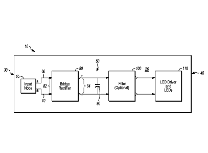
[00022] Figure 1 is a block diagram of an embodied continuous power
transmission
management system with wide range of input power on a PCB, without LED
intensity control.
CA 03073765 2020-02-24
WO 2019/046969 PCT/CA2018/051112
-6-
1000231 Figure 1A is a schematic diagram of an exemplary bridge rectifier
circuit.
Figure 1B is a schematic diagram of a few exemplary optional filter designs
for filtering conducted
and radiated emissions and voltage fluctuations.Figure 1C is a schematic
diagram of exemplary
optional filter designs for filtering inrush current.
[00024] Figure 2 is a block diagram of an embodied continuous power
transmission
management system with wide range of input power on a PCB, with LED intensity
control.
[00025] Figure 3A, 3B and 3C is a schematic diagram of more than one input
voltage
compensation circuit.
[00026] Figure 4 is a schematic diagram showing a number of
interconnected PCBs.
[00027] Figure 5 is a chart depicting the effect of a compensation circuit
in the continuous
power transmission management system.
[00028] Figure 6A-6D depicts a schematic diagram of a circuit used in
Example 1.
[00029] Figure 7 is a chart depicting the effect of a compensation circuit
on current variance
with voltage change according to one alternative.
[00030] Figure 8 is a chart depicting the effect of a compensation
circuit on LED light intensity
variance with voltage change according to one alternative.
[00031] Figure 9A-1 and 9A-2 depicts a bi-level train layout
incorporating the circuitry
according to one alternative
[00032] Figure 9B-1 and 9B-2 depicts the circuitry path of Figure 9A.
[00033] Figure 10 depicts a transit vehicle interior with a transit light
and the PCB related
thereto.
[00034] It will be appreciated that for simplicity and clarity of
illustration, elements shown in
the figures have not necessarily been drawn to scale. For example, the
dimensions of some of the
elements may be exaggerated relative to other elements for clarity. Further,
where considered
CA 03073765 2020-02-24
WO 2019/046969 PCT/CA2018/051112
- 7 -
appropriate, reference numerals may be repeated among the figures to indicate
corresponding or
analogous elements.
DETAILED DESCRIPTION
[00035] It will be appreciated that numerous specific details are set
forth in order to provide a
thorough understanding of the exemplary embodiments described herein.
[00036] However, it will be understood by those of ordinary skill in the
art that the
embodiments and/or implementations described herein may be practiced without
these specific
details. In other instances, well-known methods, procedures and components
have not been
described in detail so as not to obscure the embodiments and/or
implementations described herein.
Furthermore, this description is not to be considered as limiting the scope of
the embodiments
described herein, but rather to describe the structure and operation of the
various embodiments
and/or implementations described herein.
[00037] Referring now to FIG. 1, there is depicted a block diagram of a
continuous power
transmission management system 10, on a Printed Circuit Board (PCB) 20, having
a first end 30,
a second end 40 and a top 50, and a bottom (not shown). Proximate the first
end 30, there is a
single entry input node 65 to take AC or DC inputs 60 and 70. Connected to
inputs 60 and 70 is a
bridge rectifier 80 having an entry 82 and an exit 84. From said exit 84,
there is a capacitor 90, in
one alternative a bulky capacitor, and connected to the capacitor 90 is the
optional filter 100 which
is in communication with current load 110 that in this alternative, comprises
LED drivers and one
or more of the corresponding LEDs. Copper traces are routed in the PCB 20 to
channel passage of
power, current, and signals, individually or in combination throughout the
board and from the first
end to the second end along the longitudinal axis of the board. In one
embodiment, varying signals
are physically placed on the top 50 and the bottom (not shown) of the PCB 20
in order to minimize
noise through signals for signal passing by taking advantage of the natural di-
electrical layers of
the PCB 20 to create a capacitance between the traces.
[00038] In a preferred embodiment, the topology of the driver is a switch
mode buck. More
specifically within the family of switch mode buck regulators, the current
control method can be
either fixed-frequency, peak-current control or open-loop current mode
control. It is worth noting
CA 03073765 2020-02-24
WO 2019/046969 PCT/CA2018/051112
- 8 -
that, in one alternative, all embodiments meet at least the EN 50121-3-2 and
all requirements and
standards listed within.
[00039] In one embodiment, the bridge rectifier 80 comprises four diodes
86 connected to
create four nodes (See FIG. 1A). Two nodes 82' are each made up of an anode
and a cathode of
discrete diodes, respectively. These nodes 82 each represent voltage input to
the bridge rectifier.
A third node 84 is made up of two cathodes representing a positive output from
the bridge rectifier.
A fourth node 84 is made up of two anodes representing the negative output
(return) from the
bridge rectifier.
[00040] The bridge rectifier 80 performs the rectification of variable
power input (i.e. AC or
DC) to DC output and proper designation of output polarity. This is to ensure
the components of
the circuit function as desired. In one alternative, the voltage rating of the
diodes exceeds the
maximum required operating voltage range of the input voltage; and the current
rating of the diodes
exceeds the maximum required operating current range. In one alternative the
diodes have a
voltage rating of 1 kV (exceeding the maximum limit of voltage range of 450
volts), and a current
rating of 1.5 amps (exceeding the maximum limit of current range of 0.25
amps). Other voltage
and current ratings will be specific to the desired application.
[00041] Referring back to FIG. 1, the capacitor 90 comprises enough
capacitance to achieve a
desired "ripple" or voltage potential fluctuation to ensure a consistent
voltage resulting in
consistent performance of the current load 110. In one exemplary embodiment,
the capacitor 90
has a capacity of 33 micro Farads and a minimum voltage rating exceeding the
maximum input
voltage of the system. Also, in this exemplary embodiment, the capacitor 90
has a voltage rating
of 500 V. The positive end of the capacitor 90 is connected to the positive
output of the bridge
rectifier 80. The negative end of the capacitor 90 is connected to the
negative (return) of the bridge
rectifier 80. Other capacitors, such as ceramic capacitors that are not
polarity sensitive and may
be used as known to a person of ordinary skill in the art.
[00042] Optional filter 100 may be used to reduce at least one of the
following:
i) conducted emissions;
ii) radiated emissions;
iii) inrush current;
iv) voltage transients;
v) further voltage potential fluctuation;
CA 03073765 2020-02-24
WO 2019/046969 PCT/CA2018/051112
- 9 -
vi) and combinations thereof
[00043] Depending on the required need for the filter, each filter will
comprise various
components. A plurality of filters may be connected to each other in series.
For example the
following tables provide alternative combinations of each filter circuit as
needed. FIG. 1B is
described in the two tables as follows:
Conducted emissions filter, Radiated emissions filter, voltage fluctuation
filter
Designator Configuration 1 Configuration 2 Configuration 3
A Optional: Optional: Optional:
not populated/Capacitor not not populated/Resistor
populated/Capacitor
Resistor Inductor Inductor
Capacitor Capacitor Resistor
Transient Suppressor filter
Designator Configuration 1 Configuration 2 Configuration 3
A TVS Diode MOV Varistor
not populated not populated not populated
not populated not populated not populated
[00044] As described above, three configurations are disclosed for filters
such as conducted
emissions, radiated emissions and voltage fluctuations. Similarly, three
configurations are
disclosed for transient suppressor filters.
[00045] FIG. 1C depicts a circuit layout for filtering and/or limiting
inrush current in the PCB.
As may be seen in FIG. 1C resistor R1, diodes D1 and D2 may be optional,
resistor R2 and
transistor Q1 are mandatory.
[00046] Referring back to FIG. 1, a current load 110 is in communication
with optional filter
100. The current load 110 in this alternative comprises an LED driver and at
least one LED known
to persons of ordinary skill in the art. An example is AL9910A-5SP-13
manufactured by
DIODES Incorporated. The configuration of the circuits described in system 10
provides a
constant current source over a limited voltage range.
CA 03073765 2020-02-24
WO 2019/046969
PCT/CA2018/051112
- 10 -
[00047] FIG. 2 depicts a circuit board 25 that provides a constant
current over a wide range of
input voltage, according to another embodiment of the invention. In addition
to the components of
the PCB as described in FIG. 1, an input voltage compensation unit 120 is used
to regulate the
voltage variance and provide a constant output current to the load 110. The
input voltage
compensation unit 120 is placed between the optional filter 100 and the load
110. In the absence
of the optional filter 100, input voltage compensation unit 120 may be coupled
directly to the
capacitor 90. The output of the voltage compensation unit 120 may be connected
to the load 110
via a current sense (CS) pin 111.
[00048] Input voltage compensation circuit 120 comprises in one
alternative, as shown in FIG.
3A, at a minimum at least one biasing resistor R2 in communication with at
least one of a base or
an emitter of at least one NPN transistor, and optionally at least a resistor
R3 in communication
between a collector of said at least one NPN transistor and said at least one
current load 110.
Alternatively, FIG. 3B depicts an input voltage compensation circuit 120 of at
least one biasing
resistor in communication with at least one of a gate or a drain of at least
one N-channel MOSFET,
and optionally at least another resistor in communication between a source of
said at least one N-
channel MOSFET and said at least one current load. In the example of FIG. 3A,
where R1 = 26.5
kOhms, R2 = 10 kOhms and R3 = 0.47 kOhms, and where a CZT5551 transistor have
been used,
and in FIG. 3B where R1=111.5 kOhms, R2=10kOhms, R3=1Ohm and where a
BSZ42DN25NS3
MOSFET has been used, the following table shows the resulting current load in
the third and fourth
columns respectively for a variety of input voltages in the first column. In
FIGS. 3A, 3B and 3C,
the role of R1 is limit current and set the biasing for the transistor. The
second column lists the
current load for the same voltages without the above compensation circuit. The
current load with
the compensation circuits are considerably more uniform than the current load
without the
compensation circuit. FIG. 5 depicts a chart showing current fluctuation with
the circuit board
without a compensation circuit, with a single compensation circuit and with
multiple compensation
circuits. As can be seen the current in the board with no compensation circuit
fluctuates widely
compared to the board with a compensation circuit.
Input Voltage Current load without Current load with Simulated
(VDC) compensation circuit compensation
circuit Current load
(mA) (mA)
with N-channel
MOSFET
compensation
circuit (mA)
CA 03073765 2020-02-24
WO 2019/046969 PCT/CA2018/051112
-11-
40 356.6 329.8 331.1
60 337.5 323.4 335.3
70 327.9 321 329.5
80 321.6 321.4 324.9
90 317.1 321.9 321.4
100 314.5 324.9 319.4
110 313.9 327.4 319.3
120 311.9 330.8 317.6
[00049] FIG. 3C shows an example where the circuit of FIG. 3A includes an
additional resistor,
R4 at the output of the NPN transistor. Although not shown, a variant of FIG.
3B may also include
a resistor from the N-Channel MOSFET to the current sense pin (similar to FIG.
3C).
[00050] According to another embodiment, an alternative way to achieve
consistent intensity
over wide range of input power is to use multiple iterations of the
compensation circuit. More
number of iterations reduces output current fluctuations and variants in
response to the input
voltage range. MosFETs, op-amps or micro-controllers may be used to achieve
compensation.
[00051] The compensation network feeds into the current sense (CS) pins
of the IC, as shown
in FIGS. 2 and 3A-3C. However, similar results could be achieved if these
compensation networks
fed into the Frequency setting pin (Rosc). That would allow for a variable
switching frequency
which when configured properly could make Rosc dependent on input voltage (Eq.
2), and in turn
relieve the voltage dependency for the load current (LED in Eq.1).
[00052] In another embodiment, a negative compensation network may be
used to make use of
the Linear Dimming inputs that are typical to the wide range ICs. If making
use of a digital
dimming pin, a voltage controlled variable Pulse Width Modulation (PWM) output
circuit could
be developed. The output of this circuit would feed into the digital (PWM)
dimming input of the
IC.
[00053] Now referring to FIG. 4, a plurality of the PCBs as described
above in reference to
FIG. 2 are shown interconnected. Currently the PCB length is limited to 60" in
compliance with
the industry standards. In one embodiment, in order to achieve long runs in a
system, multiple
PCBs are combined. The PCBs are connected through end connectors 66 that
provides the on
board interconnection for creating a continuous system. As such, the overall
length of PCBs may
CA 03073765 2020-02-24
WO 2019/046969 PCT/CA2018/051112
- 12 -
vary depending on the application. Interconnection of the boards may be
enabled by any
connection type, including but not limited to SMT connectors, Blade
connectors, Poke-in
connectors, terminal blocks, and soldered wire leads.
[00054] Referring now to FIGS. 9A and 9B, Figure 9A depicts a complete
floor plan of a train
car. A singular train car consists of two sections, A car side and B car side.
There is also shown a
lower lever and upper level of a bi-level train car.
[00055] Figure 9B is a wiring diagram showing how continuous power is
passed via a single
entry point through multiple PCB boards on the upper and lower level of A car
side and B car side.
It shows that both A car side and B car side have their designated control
units. 4 output channels
are used to control power for upper and lower levels and for left and right
sides of the car.
[00056] In one alternative (See FIGS. 9A-1, 9A-2, 9B-1 and 9B-2), the
PCBs are used as
follows: PCB assemblies are installed on a bi-level train having an upper
level and a lower level. A
total of 119 PCB assemblies (or boards) are used in a continuous power
application. In this
application, the boards are split into 8 circuits; lower level A car left,
lower level A car right, upper
level A car left, upper level A car right, lower level B car left, lower level
B car right, upper level
B car left, and upper level B car right. Each one of these aforementioned
circuits has a single entry
node into its respective continuous power string. The length (and number of
boards) in each string
are respectively, 32 feet (16 boards), 32 feet (16 boards), 32 feet (16
boards), 32 feet (16 boards),
32 feet (16 boards), 22 feet (11 boards), 32 feet (16 boards) and 24 feet (12
boards). Depending
on in-service characteristics, the power fed to each of these strings can be
either 120VAC nominal
(80-140VAC), or 37.5VDC nominal (20-45VDC).
[00057] FIG. 10 depicts a typical interior of a transit vehicle with a
transit light assembly 10-
1.
[00058] Example 1
[00059] The following is an example of an alternative of the present
disclosure and how it
achieves constant LED drive current and constant LED light intensity.
[00060] EQUIPMENT
CA 03073765 2020-02-24
WO 2019/046969 PCT/CA2018/051112
- 13 -
[00061] GW Instek Power supply, model PSW160-21.6, SN:GE0215052,
Calibration
cert:40715, Calibration date: 15-Dec-16
[00062] Gigahertz-optik photo sensor, model VL-3701-4, SN: 35074,
Calibration:
1642622-WERK, Calibration date: Jan 2017
[00063] Fluke Multimeter, model 177, SN: 40820352, Calibration: 44177,
Calibration date:
24-Jan-18
[00064] PROCEDURE
[00065] Setup a light meter approximately 5 inches away from the LED
light source;
[00066] Select dial on a multimeter to mA/A position and connect it in
line with the LED string
to measure LED drive current;
[00067] Turn on the power supply and setup the input voltage at 34VDC;
[00068] Record the light level and measured LED drive current;
[00069] Increase input voltage and record the light level and LED drive
current for each of the
input voltage levels up to 168VDC.
[00070] Figure 6A-6D shows the schematic diagram of the printed circuit
board used in this
example depicting how the current sense pin CS, linear dimming pin LD,
frequency set pin RT
and pulse width modulation pin PWMD of the IC AL9910A-5SP-13 are connected
with the rest
of the circuitry to achieve the desired LED drive current and switching
frequency. A magnified
view of the LED Driver IC U2 (AL9910A-5SP-13) is shown here. The inset table
shows all the
pin numbers and pin description of IC U2. It can be seen that pin # 1 is the
input voltage pin and
is connected to Capacitor C11 (to a Pi filter). Pin # 2 is a current sense pin
and is connected to
resistor R29 which senses the switch current through the LED string and
external MOSFET. In
this experiment it is also connected to the single to multi stage compensation
network. Pin # 3 is a
GND pin and is connected to a V- node (Return path) of the circuit. Pin # 4 is
connected to the
Gate of the external MOSFET Q6(STL4N80K). Pin # 5 is a low frequency PWM
dimming pin
and is connected to capacitor C16 and pin # 6 VDD. Pin # 6 is a VDD pin which
is an internally
regulated supply voltage. Pin #6 is also connected to an external storage
capacitor C16. Pin # 7 is
a Linear Dimming input pin connected to pin VDD and capacitor C16. Pin # 8 is
a Rosc (Oscillator
CA 03073765 2020-02-24
WO 2019/046969 PCT/CA2018/051112
- 14 -
control) pin connected to a resistor R33, and used to select a desired
switching frequency. The
exposed pad on the bottom of the IC is directly connected to V- (return path)
node.
[00071] In Figure 6C, input voltage Vin is applied via connector J1.
Which is then connected
to an Inrush current limiter (ICL) R19 which limits any inrush current coming
from the input line.
The next stage is a Bridge Rectifier D39 to rectify the input voltage and a
capacitor input filter,
C10, to produce DC voltage from the rectified voltage. The next stage is an In-
rush current limiter
circuitry comprising Q2, R20, R22, D53 and D60. The resistance values of each
of R20 and R22
are chosen such that the biasing of transistor Q2 limits the In-rush current
coming from the input
line. In this example, the circuit comprising the components Q2, R20, R22, D53
and D60 is
bypassed using a jumper resistor R21. After bypassing via jumper resistor R21,
power passes
through diode D38, a reverse polarity protection diode, to the Pi filter
comprising a capacitor C9,
connected to an inductor L3 connected to a capacitor C11. Given the output
voltage coming from
the rectifier consists of AC components, it is important to remove these AC
ripples before the
voltage is applied to the Vin pin of the IC U2. The output voltage from the
Bridge Rectifier D39
is directly connected to the input capacitor C10 which provides a low
impedance path to AC ripples
present and high resistance to DC voltage. Most of the AC ripples get bypassed
through the
capacitor input stage only C10. The residual AC components which are still
present in the filtered
DC signal get filtered when they pass through inductor L3, providing high
impedance to AC and
low resistance to DC, and through capacitor Cl 1. In this manner, the
efficiency of the filtering
may be increased. When an input voltage is applied to pin # 1 of IC U2, pin #
4 (Gate pin) exhibits
a voltage higher than the threshold voltage, turning ON the external MOSFET Q6
causing the
current to flow through the LEDs, Inductor L4 and current sense resistor R29.
When the voltage
across R29 (Rsense) exceeds the current sense pin threshold the external
MOSFET Q6 is turned
off The stored energy in the inductor L4 causes current to flow through the
LEDs via re-circulative
diode D74. From the recorded data described herein, when there is no
compensation network
present, there is almost a 31% variation in the LED drive current and thus a
variation in the light
intensity over the full voltage range from 34VDC to 168VDC. A compensation
circuitry
compensates for this reduction of the LED drive current and light intensity as
the input voltage
increases from 34VDC to 168VDC. The relationship of reduction of the LED drive
current and
light intensity as the voltage increases is not linear. As the voltage
increases from 34VDC to
90VDC there is a 29% reduction in the LED drive current and light intensity
while there is
approximately 1% of fluctuation from 90VDC to 168VDC. The addition of a single
to multi stage
compensation network will compensate against this drop in the LED drive
current for a desired
input voltage range. Resisters R1 1 and R2 1 are used to configure the biasing
of MOSFET Q4.
CA 03073765 2020-02-24
WO 2019/046969
PCT/CA2018/051112
- 15 -
Similarly R1_2 and R2_2 are the biasing resistors for MOSFET Q5, R13 and R23
for MOSFET
Q1 and R14 and R2_4 for transistor Q3. As the MOSFETs Q4, Q5 and Q1 and
transistor Q3 turn
on at different input voltages due to its different biasing, Resistors R31,
R3_2, R3 3 and R3_4
get in parallel to the sense resistor R29 causing the overall Rsense to drop
resulting in an increase
in LED drive current. This increase in LED drive current works as the
compensation to the
decrease in LED drive current when there is no compensation network present
resulting in a
consistent LED drive current and light intensity.
[00072]
The table below shows a complete list of components in Figure 6A-6D of the
schematic in detail. It shows type of component, designator, quantity, value
and manufacturer
details. Other equivalent components/manufacturers may be sourced.
Component Type Designator Quantity Value
Manufacturer Manufacturer PN
Capacitor C9, C11 2 1 uF TDK
C4532X7T2E105M250KE
Capacitor C10 1 33 uF Nichicon
ULR2D330MNL1GS
Capacitor C12 1 220 pF Yageo
CC0805KRX7RABB221
Capacitor C13 1 0.1 uF TDK
C2012X7T2E104M125AE
Capacitor C16 1 2.2 uF Samsung
CL2113225KAFVPNE
D1, D2, D3, D4, D5, D6, D7,
D8, D9, D10, D11, D12, D13,
D14, D15, D16, D17, D18,
D19, D20, D21, D22, D23,
LED (light emitting D24, D25, D26, D27, D28,
diode) D29, D30 30 Seoul Semiconductor
STVV8Q14D-EMC
General purpose Diode D38, D53, D60 3 1 A ON
Semiconductor MRA4005T3
Bridge Rectifier D39 1 Fairchild
DF10S
TVS Diode D40 1 154V Littlefuse
P6SMB180CA
General purpose Diode D74 1 600V Vishay
VS-4EGU06-M3/5BT
Connector 11 1 Wago
2060-452/998-404
Inductor L3 1 220 uH Coiltronics
DR73-221-R
Inductor L4 1 680uH Bourns
5RR1208-681
N-Channel MOSFET Q1, Q4, Q5 3 STMicroelectronics
STN3N40K3
Fairchild
NPN Transistor Q2 1 Semiconductor
F1D5304DTF
NPN Transistor Q3 1 NXP Semiconductors
PZTA42,115
N-Channel MOSFET Q6 1 STMicroelectronics
STL4N80K5
100
Resistor R1_1, R1_2, R1_3 3 kOhm
Yageo RC0805FR-07100KL
12
Resistor R1_4 1 kOhm Yageo
RC0805FR-0712KL
8.25
Resistor R2_1 1 kOhm Yageo
RC0805FR-078K25L
11.8
Resistor R2_2 1 kOhm Yageo
RC0805FR-0711K8L
14.3
Resistor R2_3 1 kOhm Yageo
RC0805FR-0714K3L
Resistor R2_4 1 kOhm Yageo
RC0805FR-0720KL
CA 03073765 2020-02-24
WO 2019/046969 PCT/CA2018/051112
- 16 -
Resistor R3_1 1 33 Ohm Yageo
RC0805FR-0733RL
24.9
Resistor R3_2 1 Ohm Yageo
RC0805FR-0724R9L
Resistor R3_3 1 18 Ohm Yageo
RC0805FR-0718RL
1.43
Resistor R3_4 1 Ohm Yageo
RC0805FR-071R43L
Resistor R4_1, R4_2, R4_3, R4_4 4 0 Ohm
Stackpole Electronics RMCF0805ZTOROO
Inrush Current Limiter
(ICL) R19 1 20 Ohm EPCOS
B571535200M
249
Resistor R20 1 Ohm Yageo
RC1206FR-07249RL
Resistor R21 1 0 Ohm Stackpole Electronics
RMCF1206ZGOROO
Stackpole Electronics
Resistor R22 1 2 Ohm Inc.
RMCF1210FT2R00
Resistor R26 1 1 Ohm Stackpole Electronics
RMCF0805FT1R00
1.02
RC0805FR-071R02L
Resistor R29 1 Ohm Yageo
523
Resistor R33 1 kOhm Stackpole Electronics
RMCF0805FT523K
Resistor R34, R35 2 0 Ohm Stackpole Electronics
RMCF0805ZTOROO
LED Driver IC U2 1 Diodes Incorporated
AL9910A-5SP-13
[00073] Figure 6A also shows how a 4-stage compensation network (3 MOSFETS,
Q4, Q5 and
Q1 and 1 Transistor, Q3) is connected to the current sense pin of the IC
AL9910A-5SP-13. Without
any compensation network the LED drive current and light intensity decreases
as the Input voltage
increases from 34VDC to 168VDC. However LED drive current and light intensity
is kept
constant by connecting at least a single-stage compensation network to at
least a multi-stage
compensation network to the current sense pin of the IC AL9910A-5SP-13 as
shown in Figure 6.
Below are the recorded data outlining the benefits of various compensation
networks as per the
present disclosure.
[00074] TABULATED RESULTS
[00075]
Tables 1.1, 1.2 and 1.3 below show measured LED drive current and relative
light
intensity, respectively, over the voltage range from 34VDC to 168VDC when
there is no
compensation network.
CA 03073765 2020-02-24
WO 2019/046969
PCT/CA2018/051112
- 17 -
Minimum
current over
165 nnA
full voltage
range
Maxim urn
current over
239 mA
full voltage
range
Percentage
difference in 30.9623431
current
Table 1.1
Minimum
Relative light
intensity over 0.80045872
full voltage
range
Maximum
Relative light
intensity over 1.15366972
full voltage
range
Percentage
difference in
30.6163022 96
relative light
intensity
Table 1.2
CA 03073765 2020-02-24
WO 2019/046969 PCT/CA2018/051112
- 18 -
Without the corn pensation network ,
Drive Relative
Input Voltage
Current Light
(V)
(mA) , Intensity ,
34 239 L15366972.
35, 235.1, 1.13302752,
40 218.3 1.05504587,
45 206.6 1,
50, 198, 0.95642202,
55 191.2 0.9266055,
60 185.8 0_90137615,
65 181.2 0.88073394.
70 178 0.86009174,
75 174.8 0.85091743,
80 172.5 0.84174312.
85 171 0.82110092
90, 169.4, 0.81880734,
95, 167.6, 0.81422018,
100 166.8 0.81192661.
105 166, 0.80733945,
110 165.8 0.80504587,
115 165.4 0.80275229
120, 165.2. 0.80045872,
125 165 0.80045872,
130 165.2 0.80275229,
135. 165.2 0.80275229.
140 166 0.80504587
145 166.3 0_80963303,
150 167, 0.80963303.
155 167.6 0.81422018
160 168.2 0.81651376,
165. 168.5.. 0.81880734.
168 168.7 0.81880734
Table 1.3
[00076] Tables 2.1, 2.2 and 2.3 below show measured LED drive current and
relative light
intensity, respectively, over the voltage range from 34VDC to 168VDC when 1
transistor
compensation network is implemented.
CA 03073765 2020-02-24
WO 2019/046969
PCT/CA2018/051112
- 19 -
Minimum
current over full 203.9 nnA
voltage range
Maxim urn
current over full 225.9 mA
voltage range
Percentage
difference in 9.73882249
current
Table 2.1
Minimum
Relative light
intensity over 0.98356808
full voltage
ra nge
Maximum
Relative light
intensity over 1.08920188
full voltage
ra nge
Percentage
difference in
9.69827586
relative light
intensity
Table 2.2
CA 03073765 2020-02-24
WO 2019/046969 PCT/CA2018/051112
- 20 -
With 1 Transistor compensation network
Drive Relative Light
Input Voltage (V)
Current (mA) Intensity
(R =0.91 ), Rsens = 1, R4 = 12k,R3 = 20k
34 217.9 1.051643192
35 216.45 1.044600939
40 210.3 1.014084507
45 207 1
50 205.1 0.995305164
55 204.2 0.983568075
60 203.9 0.983568075
65 203.9 0.983568075
70 204.2 0.985915493
75 205 0.988262911
80 205.6 0.990610329
85 206.3 0.992957746
90 207.2 0.997652582
95 208 1.002347418
100 209 1.009389671
105 210 1.014084507
110 211 1.018779343
115 212.3 1.023474178
120 213.6 1.028169014
125 214.2 1.03286385
130 215.5 1.039906103
135 216.9 1.044600939
140 218.5 1.051643192
145 219.3 1.058685446
150 220.7 1.063380282
155 222.2 1.070422535
160 222.2 1.075117371
165 224.4 1.084507042
168 225.9 1.089201878
Table 2.3
[00077] Tables 3.1, 3.2 and 3.3 below show measured LED drive current and
relative light
intensity, respectively, over the voltage range from 34VDC to 168VDC when 2
Transistor
compensation networks are implemented.
CA 03073765 2020-02-24
WO 2019/046969 PCT/CA2018/051112
- 21 -
Minimum
current over full 2061. nnA
voltage range
Maxim urn
current over full 221.9 mA
voltage range
Percentage
difference in 7.12032447 %
current
Table 3.1
Minimum
Relative light
intensity over 0.98853211
full voltage
range
Maximum
Relative light
intensity over 1.066513761
full voltage
range
Percentage
difference in
7.311827957 %
relative light
intensity
Table 3.2
CA 03073765 2020-02-24
WO 2019/046969 PCT/CA2018/051112
- 22 -
With 2 Transistor compensation network
Drive Current Relative Light
Input Voltage (V)
(mA) Intensity
(R = 1.62111.62 Rsens = 1.2, R4 = 12k,R3 = 20k
34 216.3 1.041284404
35 215.2 1.03440367
40 210.8 1.016055046
45 208.1 1.
50 207 0.993119266
55 206.2 0.993119266
60 206.1 0.990825688
65 206.1 0.98853211
70 206.7 0.993119266
75 207 0.990825688
80 207.5 0.997706422.
85 208.1 1
90 208.9 1.004587156
95 209.3 1.006880734
100 210 1.006880734
105 211 1.013761468
110 211.5 1.016055046
115 212.5 1.020642202
120 213.4 1.025229358
125 213.8 1.027522936
130 213.7 1.025229358
135 214 1.029816514
140 215.3 1.032110092
145, 216.4 1.038990826
150 218 1.043577982
155 217.4 1.04587156
160 218.6 1.050458716
165 218.5 1.059633028,
168 221.9 1.066513761
Table 3.3
[00078] Tables 4.1, 4.2 and 4.3 below show measured
LED drive current and relative light
intensity, respectively, over the voltage range from 34VDC to 168VDC when 4
MOSFET
compensation networks are implemented.
CA 03073765 2020-02-24
WO 2019/046969 PCT/CA2018/051112
- 23 -
Minimum current
over full voltage 203.6 mA
range
Maximum current
over full voltage 209.7 mA
range
Percentage
difference in 2.908917501
current
Table 4.1
Minimum Relative
light intensity
0.981438515
over full voltage
range
Maximum
Relative light
1.009280742
intensity over full
voltage range
Percentage
difference in
2.75862069
relative light
intensity i
Table 4.2
CA 03073765 2020-02-24
WO 2019/046969 PCT/CA2018/051112
- 24 -
With 4 MOSFETs compensation network
Drive Current Relative Light
Input Voltage (V)
(mA) Intensity
34 207.1, 1
35 207. 1
40 207 1
45 207.3. 1
50 207 1
55 206.6 0.995359629
60 208.9 1.006960557
65 206.7, 0.995359629
70 205 0.988399072.
75 207 0.997679814
80 209.7 1.009280742
85 209.3 1.006960557
90 208 1.002320186
95 207 0.997679814
100 206 0.993039443
105 205, 0.988399072
110 204.4 0.983758701
115 204 0.983758701
120 203_6 0.981438515
125 203.6, 0.981438515
130 203.6 0.981438515
135 203.7, 0.981438515
140 204.1 0.983758701
145 204.3, 0.983758701
150 204.6 0.986078886
155 2051. 0.988399072
160 205.6, 0.990719258
165 206.1 0.993039443
168 206.8 0.995359629
Table 4.3
[00079] Tables 5.1, 5.2 and 5.3 below show measured LED drive
current and relative light
intensity, respectively, over the voltage range from 34VDC to 168VDC when 3
MOSFET & 1
Transistor compensation network is implemented.
CA 03073765 2020-02-24
WO 2019/046969
PCT/CA2018/051112
- 25 -
Minimum current
over full voltage 201.6 mA
range
Maximum current
over full voltage 209.6 mA
range
Percentage
difference in 3.816793893
current
Table 5.1
Minimum Relative
light intensity over 0.970183486
full vo Ita ge range
Maximum Relative
light intensity over 1.006880734
full vo Ita ge range
Percentage
difference in
3.644646925
relative light
intensity
Table 5.2
CA 03073765 2020-02-24
WO 2019/046969 PCT/CA2018/051112
- 26 -
With 3 MOSFETs and 1 Transistor compensation network
Relative Light
Input Voltage (V) Drive Current (mA)
Intensity
34 206.6 0.995412844,
35 206.1 0.993119266
40 206.7 0.995412844,
45 207.6 1
SO 205.3 0.98853211
55 205.8 0.990825688,
60 205.8 0.990825688,
65 204.6 0.983944954
70 203.6 0.979357798,
75 202.8 0.97706422,
80 202.3 0.972477064,
85 201.8 0.972477064
90 201.7 0.970183486,
95 201.6 0.970183486,
100 201.7 0.970183486,
105 202 0.970183486
110 202 0.972477064
115 , 202.4 0.974770642,
120 202.7 0.97706422
125 203.3 0_97706422,
130 203.9 0.981651376,
135 204.8 0.986238532,
140 205.7 0.98853211
145 , 206.5 0.993119266,
150 207.3 0.995412844
155 207.8 0.997706422
160 208.5 1.002293578,
165, 209.1 1.004587156,
168 209.6 1.006880734
Table 5.3
[00080] This example confirms when a single-stage to multi-stage
compensation network(s)
is implemented, the LED drive current and light intensity remain constant over
the full voltage
range from 34V to 168V.
[00081] From the data collected it can be seen from Figures 7 and 8
that when no compensation
network is present, the difference between the maximum drive current to
minimum drive current
over the full voltage range was 30.96% and the difference between the maximum
to minimum
relative light intensity was 30.61%.
CA 03073765 2020-02-24
WO 2019/046969 PCT/CA2018/051112
- 27 -
[00082] When 1 transistor compensation network was used, the difference
between maximum
to minimum drive current current over the full voltage range was reduced to
9.73% while the
difference between maximum to minimum relative light intensity dropped down to
9.69%.
[00083] The LED drive current and relative light intensity difference
current over the full
voltage range reduced even further to 7.12% and 7.31% respectively when a 2
transistor
compensation network was used.
[00084] The data also shows that when a 3 MOSFET and 1 transistor
compensation network
is used the difference between maximum to minimum drive current over the full
voltage range was
3.8% and difference between maximum to minimum relative light intensity
reduced to 3.6%.
[00085] Most improvement was seen when 4 MOSFET compensation network was
used, the
LED drive current difference dropped down to 2.9% and relative light intensity
difference dropped
down to 2.75% over the full voltage range. It is clear that as more
compensation networks are
implemented, the better the regulation of the drive current and light
intensity variance is achieved.
[00086] As many changes can be made to the preferred embodiment of the
disclosure without
departing from the scope thereof; it is intended that all matter contained
herein be considered
illustrative and not in a limiting sense.