Note: Descriptions are shown in the official language in which they were submitted.
CA 03074722 2020-03-04
WO 2019/055002
PCT/US2017/051366
Hybrid Kinetic Inductance Devices for Superconducting
Quantum Computing
TECHNICAL FIELD
The present disclosure relates to hybrid kinetic inductance devices for
quantum information processing systems.
BACKGROUND
Quantum computing is a relatively new computing method that takes
advantage of quantum effects, such as superposition of basis states and
entanglement
to perform certain computations more efficiently than a classical digital
computer. In
contrast to a digital computer, which stores and manipulates information in
the form
of bits (e.g., a "1" or "0"), quantum computing systems can manipulate
information
using qubits. A qubit can refer to a quantum device that enables the
superposition of
multiple states (e.g., data in both the "0" and "1" state) and/or to the
superposition of
data, itself, in the multiple states. In accordance with conventional
terminology, the
superposition of a "0" and "1" state in a quantum system may be represented,
e.g., as
a I 0> + fII>. The "0" and "1" states of a digital computer are analogous to
the I 0>
and I 1> basis states, respectively of a qubit. The value I a 12 represents
the
probability that a qubit is in 0> state, whereas the value I [3 I2 represents
the
probability that a qubit is in the I 1> basis state.
SUMMARY
In general, in some aspects, the subject matter of the present disclosure can
be
embodied in devices including: a substrate; a first superconductor layer on
the
substrate, the first superconductor layer having a first kinetic inductance;
and a second
superconductor layer on the first superconductor layer, the second
superconductor
layer having a second kinetic inductance that is lower than the first kinetic
inductance,
in which the second superconductor layer covers the first superconductor layer
such
that the second superconductor layer and the first superconductor layer have a
same
footprint, with the exception of at least a first region where the second
superconductor
layer is omitted so that the first superconductor layer and the second
superconductor
layer form a circuit element having a predetermined circuit parameter.
1
CA 03074722 2020-03-04
WO 2019/055002
PCT/US2017/051366
Implementations of the devices may include one or more of the following
features. For example, in some implementations, the second superconductor
layer
provides a lower impedance current path relative to the first superconductor
layer.
In some implementations, more than 50% of an overall inductance of the first
superconductor layer is attributed to the first kinetic inductance. In some
implementations, more than 90% of the overall inductance of the first
superconductor
layer is attributed to the first kinetic inductance. In some implementations,
less than
50% of the overall inductance of the second superconductor layer is attributed
to the
second kinetic inductance.
to In some implementations, the predetermined circuit parameter has a
resonant
frequency.
In some implementations, the predetermined circuit parameter is a center
frequency or a cut-off frequency of the circuit element.
In some implementations, the predetermined circuit parameter is a
characteristic impedance of the circuit element.
In some implementations, the circuit element includes a qubit measurement
resonator.
In some implementations, the circuit element includes a co-planar waveguide.
In some implementations, the circuit element includes a frequency filter. The
.. frequency filter may be a bandpass filter.
In some implementations, the first superconductor layer is titanium nitride.
In some implementations, the first superconductor layer is niobium nitride.
In some implementations, the first superconductor layer is a superconductor
ceramic. In some implementations, the second superconductor layer is aluminum.
In general, in another aspect, the subject matter of the present disclosure
can
be embodied in systems that include: a first superconductor trace comprising
having a
first predetermined resonator frequency; a second superconductor trace having
a
second predetermined resonator frequency that is different than the first
predetermined resonator frequency, in which each of the first superconductor
trace
and the second superconductor trace includes a first layer of a first
superconductor
material and a second layer of a second superconductor material on the first
layer, and
in which a footprint of the first superconductor trace is the same as a
footprint of the
second superconductor trace.
2
Implementations of the systems may have one or more of the following
features. For example, in some implementations, the first superconductor
material has
a first kinetic inductance, and the second superconductor material has a
second kinetic
inductance that is lower than the first kinetic inductance. For the first
superconductor
trace, a footprint of the second superconductor layer may match a footprint of
the first
superconductor layer with the exception of at least a first region where the
second
superconductor layer is omitted such that the first superconductor trace has
the first
predetermined resonator frequency. For the second superconductor trace, a
footprint
of the second superconductor layer may match a footprint of the first
superconductor
layer with the exception of at least a second region where the second
superconductor
layer is omitted such that the second superconductor trace has the second
predetermined resonator frequency. The first superconductor trace may be a
first qubit
measurement resonator, and the second superconductor trace may be a second
qubit
measurement resonator. The first superconductor trace may be a first frequency
filter
and the first predetermined resonator frequency may be a cut-off or center
frequency
of the first frequency filter, and the second superconductor trace may be a
second
frequency filter and the second predetermined resonator frequency may be a cut-
off or
center frequency of the second frequency filter.
In another aspect, there is provided a superconductor strip line comprising: a
dielectric layer; a superconductor trace embedded in the dielectric layer,
wherein the
superconductor trace comprises a first superconductor material having a first
kinetic
inductance; and a via contact within the dielectric layer and extending to the
first
superconductor trace, wherein the via contact comprises a second
superconductor
material having a second kinetic inductance that is lower than the first
kinetic
inductance.
In some implementations, more than 50% of an overall inductance of the first
superconductor material is attributed to the first kinetic inductance. In some
implementations, more than 90% of the overall inductance of the first
superconductor
material is attributed to the first kinetic inductance. In some
implementations, less
than 50% of the overall inductance of the second superconductor material is
attributed
to the second kinetic inductance.
3
Date Recue/Date Received 2021-09-24
In some implementations, an inductance per unit length of the first
superconductor material is higher than an inductance per unit length of the
second
superconductor material.
In general, in other aspects, the subject matter of the present disclosure can
be
embodied in devices that include: a substrate; and a circuit element including
a
superconductor trace on the substrate, in which more than 50% of an overall
inductance of the superconductor trace is attributed to a kinetic inductance
of a
superconducting material forming the superconductor trace, a first region of
the
superconductor trace has a first cross-sectional area exhibiting a first
kinetic
inductance, and a second region of the superconductor trace has a second cross-
sectional area exhibiting a second kinetic inductance, the first cross-
sectional area
being different from the second cross-sectional area such that the first
kinetic
inductance is different than the second kinetic inductance and such that the
circuit
element has a predetermined circuit parameter.
Implementations of the devices may have one or more of the following
features. For example, in some implementations, the predeteimined circuit
parameter
is a resonant frequency. In some implementations, the superconductor material
includes titanium nitride, niobium nitride or a superconductor ceramic.
In some implementations, the circuit element includes a qubit measurement
resonator.
In some implementations, the circuit element includes a frequency filter.
In some implementations, more than 90% of the overall inductance of the
superconductor trace is attributed to the kinetic inductance of the
superconductor
material.
In some implementations, the superconductor trace consists of the
superconductor material.
In another aspect, there is provided a kinetic inductance device comprising: a
substrate; a first superconductor layer on the substrate, the first
superconductor layer
having a first kinetic inductance; and a second superconductor layer on the
first
superconductor layer, the second superconductor layer having a second kinetic
inductance that is lower than the first kinetic inductance, wherein the second
superconductor layer covers the first superconductor layer such that the
second
superconductor layer and the first superconductor layer have a same footprint,
with
4
Date Recue/Date Received 2021-09-24
the exception of at least a first region where the second superconductor layer
is
omitted so that the first superconductor layer and the second superconductor
layer
form a circuit element having a predetermined circuit parameter, wherein the
circuit
parameter is a resonant frequency, a center frequency, a cut-off frequency, or
a
characteristic impedance of the circuit element.
In another aspect, there is provided a kinetic inductance device comprising: a
substrate; and a circuit element comprising a superconductor trace on the
substrate,
wherein more than 50% of an overall inductance of the superconductor trace is
attributed to a kinetic inductance of a superconducting material forming the
superconductor trace, a first region of the superconductor trace has a first
cross-
sectional area exhibiting a first kinetic inductance, and a second region of
the
superconductor trace has a second cross-sectional area exhibiting a second
kinetic
inductance, the first cross-sectional area being different from the second
cross-
sectional area such that the first kinetic inductance is different than the
second kinetic
inductance and such that the circuit element has a predetermined circuit
parameter,
wherein the circuit parameter is a resonant frequency, a center frequency, a
cut-off
frequency, or a characteristic impedance of the circuit element.
Particular implementations of the subject matter described here can realize
one
or more of the following advantages. For example, in some implementations, it
is
possible to fabricate circuit elements of the same type (e.g., qubit, qubit
measurement
resonator, co-planar waveguide, and signal trace, among other circuit element
types)
having different predetermined resonance properties without substantially
different
geometric dimensions. By forming circuit elements, at least in part, from high
kinetic
inductance materials, it is possible in some implementations to reduce the
design
complexity of quantum infoimation processing systems. In particular, circuit
elements
of the same type may be formed to have different resonance properties, without
requiring different sizes or the use of different materials among each of the
various
circuit elements. Moreover, fabricating circuit elements to have the same size
but
different resonance properties can, in some implementations, free up space and
allow
for an increase in the density of the circuit elements within a quantum
information
processing system. Furthermore, in some implementations, forming a circuit
element,
at least in part, from high kinetic inductance materials allows the circuit
element to
5
Date Regue/Date Received 2022-07-25
have predetermined resonance properties in a more compact geometry relative to
the
same circuit element fabricated without high kinetic inductance material.
The details of one or more implementations are set forth in the accompanying
drawings and the description below. Other features and advantages will be
apparent
from the description, the drawings, and the claims.
BRIEF DESCRIPTION OF THE DRAWINGS
FIG. lA is a schematic illustrating a plan-view and a cross-section view (at
line A-A) of an example of a first circuit element.
FIG. 1B is a schematic illustrating a plan-view and a cross-section view (at
line B-B) of an example of a second circuit element.
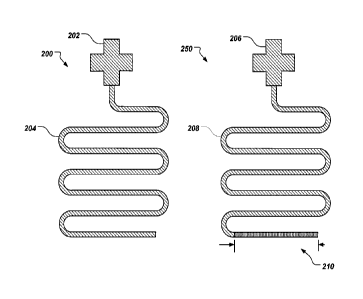
FIG. 2 is a schematic illustrating a plan view of an example of a system that
includes qubits and measurement resonators fabricated, at least in part, from
a high
kinetic conductance material.
FIGS. 3A and 3B are schematics illustrating plan-views of an example of a
first superconductor measurement resonator and an example of a second
superconductor measurement resonator, respectively.
FIG. 4 is a schematic illustrating an example of a circuit element formed from
a superconducting material having a high kinetic inductance.
FIG. 5 is a schematic that illustrates a plan view and a cross-section view
through line A-A of an example of a strip line design for a superconducting
quantum
information processing system.
DETAILED DESCRIPTION
Quantum computing entails coherently processing quantum information stored
in the quantum bits (qubits) of a quantum infoimation processing system. As
the
5a
Date Regue/Date Received 2022-07-25
CA 03074722 2020-03-04
WO 2019/055002
PCT/US2017/051366
number of qubits within a quantum information processing system increases, the
computational capabilities of the system increases substantially, potentially
providing
processing power far exceeding that of classical computing systems for certain
complex problems.
Superconducting quantum information processing systems may include circuit
elements that are formed using superconducting materials and that are
principally
controlled through the application of microwave signals in the range of
several
hundred MHz to several hundred GHz, such as between 500 MHz -20 GHz. In some
implementations, the circuit elements of a superconducting quantum information
processing system, such as the qubits, may exhibit "resonance" conditions in
which
the microwave control signals are used to drive transitions between different
states
(e.g., the different states of a qubit). Additionally, microwaves may be used
to
measure the state of a qubit through a measurement resonator coupled to the
qubit.
The resonance conditions and resonance frequencies associated with such
circuit
elements of a superconducting quantum information processing system are
related to
the overall inductance associated with the circuit elements. Thus, one way to
modify
the resonance condition and/or resonance frequency is to change the overall
inductance of the circuit element by altering the geometry of the circuit
element.
Alternatively, as disclosed herein, the overall inductance, and thus the
resonance properties, of circuit elements may be modified by forming the
circuit
elements, at least in part, from materials exhibiting high kinetic inductance,
LK.
Kinetic inductance is the manifestation of the inertial mass of mobile charge
carriers
in alternating electric fields as an equivalent series inductance. Kinetic
inductance
may be observed at very high frequencies (e.g., in the microwave frequency
range) in
high carrier mobility conductors and superconductors. Kinetic inductance
contrasts
with geometric magnetic inductance in a superconductor, Liti, which relates to
the
energy stored due to the magnetic field induced by the applied current, and
which
depends on the geometry of the conductor. Geometric inductance therefore is
material
independent, whereas kinetic inductance is material dependent. For the general
case
of the superconducting strip of width Wand thickness t, the kinetic inductance
per
tioAf,
unit length LK may be expressed as LK = wt , where ,uo is the vacuum
permeability
and AL is the London penetration depth. Similarly, for a superconducting
coplanar
6
CA 03074722 2020-03-04
WO 2019/055002
PCT/US2017/051366
waveguide resonator, the kinetic inductance may be expressed as LK = g,
where
g is a function of the center trace width W, the center trace thickness 1, and
the
spacing width s between the center trace and the ground planes. Since the
inductance
depends on both width and length of a trace, the kinetic inductance also may
be
expressed as an inductance per square. For a superconducting material, the
total
inductance per unit length may be expressed as L =LA4- + LK. For certain
superconductors, the value of geometric magnetic inductance is negligible
compared
to the kinetic inductance such that L golx. Accordingly, for the example of a
co-planar
waveguide, the overall inductance of the waveguide may be attributed to a
geometric
to inductance per unit length which comes from the width to gap ratio of
the co-planar
waveguide, and to a kinetic inductance per square, which varies according to
the
material used for the waveguide and is independent of the geometric inductance
(but
also depends on the waveguide geometry).
While the kinetic inductance of a superconductor material also may vary with
temperature, the kinetic inductances referred to herein correspond to the
values
exhibited in an environment that is at or below the critical temperature of
the
superconductors with which the kinetic inductance is associated, and are
generally
constant in such temperature regimes.
By using materials exhibiting high kinetic inductance at the frequencies
(e.g.,
between 500 MHz -20 GHz) typically applied in superconducting quantum
information processing systems, it is possible, in some implementations, to
fabricate
circuit elements of the same type (e.g., qubit, qubit measurement resonator,
co-planar
waveguide, and signal trace, among other circuit element types) having
different
predetermined resonance properties without substantially different geometric
dimensions. For example, a superconducting circuit element may be formed to
have a
first set of geometric dimensions (e.g., length and width) and a first
predetermined
resonance frequency, while a second superconducting circuit element may be
formed
to have the same geometric dimensions (e.g., length and width) as the first
qubit
measurement resonator but a different predetermined resonance frequency by
altering
the amount of high kinetic inductance material that contributes to the overall
inductance of the second superconducting circuit element.
By folining circuit elements, at least in part, from high kinetic inductance
materials, it is possible in some implementations to reduce the design
complexity of
7
CA 03074722 2020-03-04
WO 2019/055002
PCT/US2017/051366
quantum information processing systems. In particular, circuit elements of the
same
type may be formed to have different resonance properties, without requiring
different
sizes or the use of different materials among each of the various circuit
elements.
Moreover, fabricating circuit elements to have the same size but different
resonance
properties can, in some implementations, free up space and allow for an
increase in
the density of the circuit elements within a quantum information processing
system.
Furthemiore, in some implementations, forming a circuit element, at least in
part,
from high kinetic inductance materials allows the circuit element to have
predetermined resonance properties in a more compact geometry relative to the
same
circuit element fabricated without high kinetic inductance material.
FIG. 1A is a schematic illustrating a plan-view and a cross-section view (at
line A-A) of an example of a first circuit element 100, and FIG. 1B is a
schematic
illustrating a plan-view and a cross-section view (at line B-B) of an example
of a
second circuit element 150. Each of the first circuit element 100 and the
second
circuit element 150 may be, e.g., a thin-film signal trace. Signal traces may
be used in
quantum information processing devices to transmit signals to and from control
and
data circuit elements. For instance, in some implementations, a signal trace
forms part
of a co-planar waveguide, such as the center trace that is laterally bounded
on either
side by an air gap and a ground plane. Such a co-planar waveguide may be
coupled to
a qubit to provide the qubit with one or more control signals for causing a
transition
between different qubit states. In some implementations, a signal trace forms
part of a
qubit measurement resonator for reading out the state of a qubit. In some
implementations, a signal trace forms part of a qubit coupling element for
inductively
or capacitively coupling two or more qubits or other circuit elements
together. In
some implementations, a signal trace is part of a stripline configuration
rather than
part of a co-planar waveguide. That is, the signal trace is embedded in a
dielectric
substrate bounded on the top and bottom by a ground plane.
Each of the first circuit element 100 and the second circuit element 150 is
formed on a dielectric substrate 102, such as a silicon or sapphire wafer. The
first
circuit element 100 has a width 101 and a length 103, whereas the second
circuit
element 150 has a width 107 and a length 109. A footprint of the first circuit
element
100 corresponds to the area of the substrate surface defined by the width 101
and
8
CA 03074722 2020-03-04
WO 2019/055002
PCT/US2017/051366
length 103. A footprint of the second circuit element 150 corresponds to the
area of
the substrate surface defined by the width 107 and length 109.
Furthermore, as shown in the cross-sections of FIGS. IA-1B, each of the first
circuit element 100 and the second circuit element 150 includes a bi-layer of
material.
That is, each of the first circuit element 100 and the second circuit element
150
includes a first layer 108 on the substrate 102 and a second layer 110 on the
first layer
108. In the first circuit element 100, the second layer 110 completely covers
the upper
surface of the first layer 108. In the second circuit element 150, a first
portion or
region 120 is devoid of the second layer 110 to reveal/expose the upper
surface of the
to .. first layer 108. In a second portion or region 130 of the circuit
element 150, the
second layer 110 covers the upper surface of the first layer 108.
The first layer 108 is formed from a material having a high kinetic inductance
relative to the kinetic inductance of the material that forms the second layer
110. For
example, the first layer 108 may be formed from a material that exhibits a
high kinetic
inductance, including superconductors and/or ceramics such as, e.g., titanium
nitride,
niobium titanium nitride, niobium nitride, tungsten silicide, platinum
silicide, and
superconducting aluminum oxide. The second layer 110 may be formed from a
material that exhibits no or much less kinetic inductance than the material of
the first
layer 108 including materials such as, e.g., aluminum, indium, molybdenum and
ruthenium. While kinetic inductance can vary with frequency, in
superconducting
systems in the 50 MHz to 20 GHz range, kinetic inductance, for a fixed element
size,
is a constant of the material depending on the London penetration depth. As
explained herein, superconducting quantum information processing systems
entail the
application of signals in the microwave frequency range such as, e.g., between
300
Miliz and 300 GHz, including between 500 MHz and 20 GHz. Thus, for the
examples
set forth herein, a superconducting material is understood to have a "high" or
a "low"
kinetic inductance value for applied electromagnetic fields within the
microwave
frequency range (e.g., between 500 MHz and 20 GHz) and at temperatures at or
below the critical temperature of the superconducting material.
In some implementations, the first laver 108 may be formed from a material
having a first kinetic inductance, whereas the second layer 110 may be formed
from a
material having a second different kinetic inductance. In some
implementations, an
overall inductance of the first layer 108 is attributed to both the first
kinetic
9
CA 03074722 2020-03-04
WO 2019/055002
PCT/US2017/051366
inductance LK/ and to the geometric magnetic inductance Livf. For example, in
some
implementations, more than 50% of an overall inductance L of the first layer
108 is
attributed to the first kinetic inductance Lri, more than 60% of an overall
inductance
L of the first layer 108 is attributed to the first kinetic inductance LK],
more than 70%
of an overall inductance L of the first layer 108 is attributed to the first
kinetic
inductance LK1, more than 80% of an overall inductance L of the first layer
108 is
attributed to the first kinetic inductance LK1, or more than 90% of an overall
inductance L of the first layer 108 is attributed to the first kinetic
inductance Liu.
Similarly, in some implementations, the overall inductance of the second
layer 110 is attributed both to the second kinetic inductance LK2 and to the
geometric
magnetic inductance resulting from the second layer's shape, independent of
material.
For example, in some implementations, less than 50% of the overall inductance
L of
the second layer 110 is attlibuted to the second kinetic inductance LK2, less
than 40%
of the overall inductance L of the second layer 110 is attributed to the
second kinetic
inductance LK2, less than 30% of the overall inductance L of the second layer
110 is
attributed to the second kinetic inductance LK2, less than 20% of the overall
inductance L of the second layer 110 is attributed to the second kinetic
inductance
LK2, or less than 10% of the overall inductance L of the second layer 110 is
attributed
to the second kinetic inductance LK2.
When a time-varying electric or magnetic field is applied to each of the first
circuit element 100 and the second circuit element 150, a current may be
generated in
each of the first circuit element 100 and in the second circuit element 150.
The second
layer 110 provides a provides a lower impedance current path relative to the
first layer
108 so that electric current travels primarily through the second layer 110
(negligible
levels of current may travel through the first layer 108). That is, current
travels
primarily through the material exhibiting a zero or low kinetic inductance
relative to
the material exhibiting high kinetic inductance. The second layer 110
effectively acts
as a short circuit around the first layer 108. Since the second layer 110 has
zero or a
relatively low kinetic inductance (e.g., less than 50% of the overall
inductance
attributed to kinetic inductance), the overall inductance of the first circuit
element 100
may be determined primarily by the inductance resulting from the second
layer's
geometric inductance (derived from the magnetic permeability and shape) of the
material forming the second layer 110.
CA 03074722 2020-03-04
WO 2019/055002
PCT/US2017/051366
In contrast, as explained herein, in the second circuit element 150, a first
portion or region 120 is devoid of the second layer 110 to reveal/expose the
upper
surface of the first layer 108. In a second portion or region 130 of the
circuit element
150, the second layer 110 covers the upper surface of the first layer 108.
Again, the
second layer 110 provides a lower impedance current path relative to the first
layer
108. Accordingly, upon the application of a time-varying electric or magnetic
field
having a frequency in the microwave frequency range to the second circuit
element
150, the current primarily travels through the second layer 110 in the second
region
130 and travels through the first layer 108 in the first region 120. That is,
the current
io primarily travels through the material exhibiting zero or low kinetic
inductance in
region 130, and travels through the material exhibiting high kinetic
inductance in
region 120. The second layer 110 effectively acts a short circuit around the
first layer
108 in region 130. Thus, the overall inductance of the second circuit element
150 is
determined by the inductance and shape (e.g., length, width and height) of the
second
layer 110 in the region 130, and by the kinetic inductance of the first layer
108 in the
region 120.
As explained herein, in some implementations, the overall inductance of the
first layer 108 may be substantially due to its kinetic inductance value
rather than the
inductance due to the material's magnetic permeability. For instance, more
than 90%
of the overall inductance of the first layer 108 may be attributed to its
kinetic
inductance.
Because the kinetic inductance of the first layer 108 is high relative to the
geometric inductance of that layer, the kinetic inductance significantly
increases the
overall inductance of the circuit element. As a result, the second circuit
element may
be formed to have the same length 109 and width 107 of the second circuit
element
150 can be made equal to the length 103 and width 101, respectively, of the
first
circuit element 100, using the same materials (e.g., aluminum and titanium
nitride),
but result in the first circuit element exhibiting a different overall
inductance, and thus
different resonant properties such as resonant frequency, from the overall
inductance
of the second circuit element 150. That is, the first circuit element 100 and
the second
circuit element 150 may have the same footprint on the substrate surface,
using the
same materials, but have different predetermined circuit parameters (e.g.,
different
overall inductance and resonant properties or different characteristic
impedance). It
11
CA 03074722 2020-03-04
WO 2019/055002
PCT/US2017/051366
follows that by altering the amount of the first layer (which exhibits a high
kinetic
inductance) that is exposed or uncovered by the second layer (which exhibits a
low or
zero kinetic inductance), it is possible to alter circuit parameters (e.g.,
overall
inductance and resonant properties) of a circuit element without altering the
footprint
of the circuit element on the substrate surface.
As explained with respect to FIG. 1, the circuit elements 100, 150 may form
part of a qubit measurement resonator for reading out the state of a qubit.
FIG. 2 is a
schematic illustrating a plan view of an example of a system that includes
qubits and
measurement resonators fabricated, at least in part, from a high kinetic
conductance
to .. material. In particular, FIG. 2 illustrates an example of a first qubit-
measurement
resonator pair 200 and a second adjacent qubit-measurement resonator pair 250.
The
first qubit-measurement resonator pair 200 includes a qubit 202 and a
measurement
resonator 204 coupled (e.g., through a direct electrical connection, a
capacitive
coupling, or an inductive coupling) to the qubit 202. The second qubit-
measurement
resonator pair 250 includes a qubit 206 and a measurement resonator 208
coupled
(e.g., through a direct electrical connection, a capacitive coupling, or an
inductive
coupling) to an end of the qubit 206. Each of the qubit 202 and the qubit 206
may
include a superconducting qubit, such as a phase qubit, a charge qubit, or a
flux qubit
(e.g., a co-planar waveguide flux qubit). Furthermore, each of the measurement
resonator 204 and 208 is a co-planar waveguide. For ease of viewing, the
ground
plane is omitted and only the center conductors of the co-planar waveguides
are
shown in FIG. 2. Each of the measurement resonator 204 and 208 is formed, at
least
in part, from a thin film bi-layer. That is, each measurement resonator 204,
208
includes a first layer of superconductor material having a first kinetic
inductance, and
.. a second layer of superconductor material on the first layer of
superconductor
material, in which the second layer of superconductor material has a second
kinetic
inductance. The first kinetic inductance is higher than the second kinetic
inductance in
the microwave frequency range (e.g., between 500 MI-1z and 20 GHz). For
example,
the first layer of each measurement resonator may include titanium nitride,
niobium
nitride or superconducting aluminum oxide, whereas the second layer may
include
aluminum. The thickness of the first layer of superconductor material in each
measurement resonator 204 and 208 may be the same. Similarly, the thickness of
the
second superconductor layer, where the second layer is provided, in each
12
CA 03074722 2020-03-04
WO 2019/055002
PCT/US2017/051366
measurement resonator 204 and 208 may be the same. For instance, the thickness
of
the first layer of superconductor material in each resonator may be between
several
nanometers to approximately 100 nanometers, whereas the thickness of the
second
layer of superconductor material in each resonator may be between
approximately ten
nanometers and approximately several microns. Thus, the first measurement
resonator
204 and the second measurement resonator 208 are formed from a bi-layer
similar to
that shown in FIG. 1 for the signal trace. The devices shown in FIG. 2 are
fabricated
on a dielectric substrate, such as silicon or sapphire.
Each of the first measurement resonator 204 and the second measurement
resonator 208 has the same center conductor length /, corresponding to a path
length
between an end of the center conductor proximal to the qubit to which the
resonator is
coupled and an end of the center conductor that is distal from the qubit to
which the
resonator is coupled. Each of the first measurement resonator 204 and the
second
measurement resonator 208 also has the same center conductor linewidth w.
Furthermore, a gap width between the center conductors and adjacent ground
planes
is the same. Accordingly, both the first measurement resonator 204 and the
second
measurement resonator 208 have the same footprint.
As shown in FIG. 2, a difference between the first measurement resonator 204
and the second measurement resonator 208 is that the second measurement
resonator
208 includes a region 210 of the central conductor having a length s, in which
the
second superconductor layer is absent or has been removed to expose/reveal the
first
superconductor layer. For the first measurement resonator 204, when a time-
varying
electric field having a predetermined frequency is applied (e.g., in the
microwave
frequency range), current will travel primarily through the second
superconductor
layer due to the second superconductor layer's lower overall impedance
relative to the
first superconductor layer. Thus, the first measurement resonator 204 will
exhibit a
fundamental resonator frequency foi that is based on the inductance L2 of the
second
superconductor layer. For example, for a quarter wave qubit readout resonator,
the
resonator frequencyfin may be expressed as hi = 1/(4sVL2C), where C is the
capacitance per unit length. For a bandpass filter, ./0] may be expressed as
fen =
1/(2s /..s!').
In contrast, for the second measurement resonator 208, when a time-varying
electric field having the predetermined frequency (e.g., in the microwave
frequency
13
CA 03074722 2020-03-04
WO 2019/055002
PCT/US2017/051366
range) is applied, current will travel primarily through the second
superconductor
layer only through the portion of the central conductor that includes the
second
superconductor layer. For the portion 210 of the central conductor where the
second
superconductor layer is absent or removed, current travels through the first
superconductor layer. The second measurement resonator 208 thus exhibits an
overall
inductance based on the inductance L2 of the second superconductor layer where
the
second superconductor layer is present, and based on the inductance Li of the
first
superconductor layer where the second superconductor layer is absent. The
inductance L2 of the second superconductor layer for resonator 208 may be
primarily
to attributed to its geometric inductance. The inductance Li of the first
superconductor
layer for resonator 208 may be expressed as a function of the first
superconductor
layer's kinetic inductance and geometric inductance attributable to the shape
of the
first superconductor layer in the region in which the second superconductor
layer is
absent. For example, more than 50%, more than 60%, more than 70%, more than
80%, or more than 90% of the inductance of the first superconductor layer may
be
attributed to the kinetic inductance of the material forming the first
superconductor
layer. Because of the portion 210 exposing the high kinetic inductance
material, the
overall inductance of the second measurement resonator will be higher than the
overall inductance of the first measurement resonator. Furthermore, the
fundamental
resonator frequency fo2 of resonator 208 may be expressed as a function of (Li
+ L2).
For example, for a quarter wave qubit readout resonator, the resonator
frequency fi9i
may be expressed as f02 = 1/44(L1 + L2)C, where s is the trace length and C is
the
capacitance per unit length. For a bandpass filter, the frequency would be
half of the
quarter wave qubit readout resonator frequency. The system shown in FIG. 2
therefore includes two qubit measurement resonators each having the same
footprint
on the substrate, but different fundamental operating frequencies, allowing
simplification and uniform design of a quantum information processing system.
Though FIG. 2 shows examples of qubit measurement resonators, the subject
matter of the present disclosure may be applied to other types of resonators
as well.
For example, in some implementations, multiple bandpass filters may be formed,
in
which each bandpass resonator includes a thin film hi-layer having the same
overall
footprint on a substrate, but where the coverage of a second superconductor
layer
exhibiting a low kinetic inductance over a first superconductor layer
exhibiting a high
14
CA 03074722 2020-03-04
WO 2019/055002
PCT/US2017/051366
kinetic inductance differs among the bandpass resonators. A readout resonator
has one
end of the resonator shorted to ground and an opposite end open, whereas a
bandpass
filter has both ends of the resonator open. By altering the coverage of the
second
superconductor layer having the low kinetic inductance, the bandpass
resonators may
exhibit different center frequencies.
Similarly, in some implementations, multiple low pass filters may be formed,
in which each low pass filter includes a thin film bi-layer having the same
overall
footprint on a substrate, but where the coverage of a second superconductor
layer
exhibiting a low kinetic inductance over a first superconductor layer
exhibiting a high
kinetic inductance differs among the low pass filters. By altering the
coverage of the
second superconductor layer having the low kinetic inductance, the low pass
filters
resonators may exhibit different cutoff frequencies.
Similarly, in some implementations, multiple high pass filters may be formed,
in which each high pass filter includes a thin film bi-layer having the same
overall
footprint on a substrate, but where the coverage of a second superconductor
layer
exhibiting a low kinetic inductance over a first superconductor layer
exhibiting a high
kinetic inductance differs among the high pass filters. By altering the
coverage of the
second superconductor layer having the low kinetic inductance, the high pass
filters
resonators may exhibit different cutoff frequencies.
The use of superconductor materials having high kinetic inductance also
allows forming more compact circuit elements that exhibit the same inductance,
and
thus the same resonance properties, as larger circuit elements formed from
materials
having lower kinetic inductance. FIGS. 3A and 3B are schematics illustrating
plan-
views of a first superconductor measurement resonator 300 and a second
superconductor measurement resonator 350, respectively. As with the
measurement
resonators of FIG. 2, each of the first and second measurement resonators 300,
350
includes a center conductor laterally separated from a ground plane by a
constant gap
width. For ease of viewing, the ground planes are omitted from FIGS. 3A and
3B. In
contrast to the resonators of FIG. 2, however, the first measurement resonator
300 and
the second measurement resonator 350 are not formed from bilayer films having
both
low kinetic inductance and high kinetic inductance materials. Rather, the
first
measurement resonator 300 is formed entirely from a thin film (e.g.,
approximately
several nm to approximately 2 microns) of superconductor material having a low
CA 03074722 2020-03-04
WO 2019/055002
PCT/US2017/051366
kinetic inductance at a predetermined frequency (e.g., between 500 MHz ¨ 20
GHz)
of an applied electric field, such as aluminum. The second measurement
resonator 350
is formed entirely from a thin film (e.g., approximately several nm to
approximately-
2 microns) of superconductor material having a high kinetic inductance (e.g.,
a kinetic
inductance ratio of 9:1 compared to the kinetic inductance of the material
forming
resonator 300) at the predetermined frequency, such as titanium nitride or
niobium
nitride. As shown in FIGS. 3A and 3B, the first measurement resonator 300 has
a
much longer center trace length than the second measurement resonator 350. Due
to
the higher kinetic inductance of the material constituting resonator 350
relative to the
to kinetic inductance of the material constituting resonator 300, the
resonator 350 may
be formed to provide the same overall inductance as resonator 300, but with a
much
shorter center trace length. In some implementations, forming a quantum
information
processing device, such as a qubit measurement resonator, entirely out of a
high
kinetic inductance material may unintentionally distort low frequency
waveforms
(e.g., between 0 and about 300 MHz) applied to the device, whereas quantum
information processing devices formed from both high and low kinetic
inductance
materials (e.g., both superconductors) may induce less waveform distortion
given that
the lower kinetic inductance material serves to provide a lower impedance
pathway
around the high kinetic inductance material.
FIG. 4 is a schematic illustrating an example of a circuit element 400 (e.g.,
a
qubit measurement resonator) foinied from a superconducting material having a
high
kinetic inductance, in which the value of kinetic inductance in the circuit
element
varies in different regions by modifying a geometric dimension (e.g.,
thickness of the
circuit element) of the circuit element in those regions. FIG. 4 shows a plan
view of
the qubit measurement resonator 400 and a cross-section view through line A-A
of the
resonator 400. Similar to resonator 200, resonator 400 includes a center
conductor
laterally separated from a ground plane by a constant gap width, For ease of
viewing,
the ground plane is omitted from FIG. 4. The resonator 400 is formed entirely
of a
superconductor material 402 exhibiting a high kinetic inductance in the
frequency
range of about 500 MHz ¨ 20 GHz. For example, in some implementations, the
resonator 400 is formed from titanium nitride or niobium nitride.
As shown in the cross-section view of FIG. 4, the thickness of the resonator
400 varies along the length of the central conductor from a first end to a
second end.
16
CA 03074722 2020-03-04
WO 2019/055002
PCT/US2017/051366
That is, in a first region 406, the thickness of the superconductor material
402 has a
first thickness (e.g., 500 nm). In a second region 408, the superconductor
material 402
is thinned to have a second thickness (e.g., 100 nm) that is less than the
first thickness.
In a third region 410, the superconductor material 402 is thinned further to
have a
third thickness (e.g., 20 nm) that is less than both the first and second
thickness. As
the thickness of the resonator 400 decreases from region 406 to 410, the
kinetic
inductance per unit length associated with each region increases. For example,
the
value of kinetic inductance per unit length in region 406 may be higher than
the
kinetic inductance per unit length in regions 408 and 410, whereas the value
of kinetic
to inductance per unit length in region 408 may be higher than the kinetic
inductance per
unit length in region 410. The overall inductance of the resonator 400 then
may be
determined, in certain implementations, based on the particular kinetic
inductance
values exhibited in each of regions 406, 408 and 410. Thus, altering a
thickness of a
superconductor along its length provides another approach for varying the
overall
inductance of a circuit element, without needing to vary the footprint of the
circuit
element.
For instance, in some implementations, a system may include multiple
quantum information processing devices of the same type (e.g., qubit
measurement
resonators), each having the same footprint on a substrate (e.g., same length
and same
width of a central conductor path). Each device also may be formed from a
material
having a high kinetic inductance at a predetermined frequency (e.g., titanium
nitride
or niobium nitride under applied electric fields with a frequency between 500
MHz ¨
20 GHz). The overall inductance, and thus the resonant properties (e.g.,
central
frequency), of each of the quantum information processing devices then may be
varied by changing the amount of high kinetic inductance material (e.g., by
changing
the thickness of the high kinetic inductance material) in one or more
different regions
along the device without altering the footprint of the device on the
substrate.
In some implementations, combining materials exhibiting high kinetic
inductance with materials exhibiting low kinetic inductance may be used to
alter the
characteristic impedance of circuit elements, e.g., for performing impedance
matching. For example, a strip line will have substantially different
impedance from a
co-planar waveguide of the same length because of the lower capacitance per
unit
length of the co-planar waveguide.. As a result, when a strip line is
connected to a co-
17
CA 03074722 2020-03-04
WO 2019/055002
PCT/US2017/051366
planar waveguide having a different impedance, this may result in signal back
reflectance. To reduce the back reflectance, the co-planar waveguide and the
signal
line can be fottned to have the same impedance. For example, the inductance L
of the
signal trace can be increased so that its impedance (which can be expressed as
VL/C )
matches the impedance of the co-planar waveguide. For instance, in some
implementations, it may be desirable to set the impedance of the strip line to
50 ohms
or 75 ohms so that it matches standard impedance values used with microwave
components. For a strip line, this may be accomplished by narrowing the width
of the
signal line to compensate for the higher capacitance per unit length or moving
the
io ground planes further away from the signal line to reduce the
capacitance per unit
length. However, such an approach may require forming the signal line so
narrow or
the ground planes so far away that it the strip line is difficult to
fabricate. An
alternative technique for modifying the impedance of the strip line is to
increase the
inductance of the signal trace by forming the signal trace from a
superconducting
material having a high kinetic inductance. The signal line then may be formed
wider
and thus easier to fabricate while providing an impedance that can match the
impedance of the co-planar waveguide, and/or of other components.
FIG. 5 is a schematic that illustrates a plan view and a cross-section view
through line A-A of an example of a strip line design for a superconducting
quantum
information processing system. For example, the strip line 500 shown in FIG. 5
can
be used to carry data and/or control signals to and/or from a qubit, a qubit
measurement resonator, or a qubit coupler. The strip line 500 includes a first
superconducting layer 500 formed on a first principal surface of a substrate
504 (e.g.,
the upper surface of substrate 504), a second superconducting layer 506 formed
on a
second principal surface of substrate 504 (e.g., the lower surface of
substrate 504), a
superconducting signal trace 508 embedded within the substrate 504, and a
superconducting via contact 510 formed within the substrate 504 and connecting
to
the signal trace 508. Each of the first and second superconducting layers 502,
506
may be formed from a superconducting material having either low or high
kinetic
inductance. For example, layers 502, 506 may be formed from aluminum, niobium
nitride, or titanium nitride. Each of layers 502, 506 serves as a shielding
ground plane
for signal trace 508. Signal trace 508 is formed from a first superconductor
material
having a high kinetic inductance, such as titanium nitride, niobium nitride,
tungsten
18
CA 03074722 2020-03-04
WO 2019/055002
PCT/US2017/051366
suicide, or superconducting aluminum oxide. For example, more than 50% of an
overall inductance of the first superconductor material 508 may be attributed
to
kinetic inductance, or more than 90% of the overall inductance of the first
superconductor material 508 may be attributed to kinetic inductance. The width
of the
strip line (e.g., as defined into and out of the page of the figure) 500 may
be in the
range, e.g., of between approximately several hundred nanometers to
approximately
several microns. The thickness of the strip line (e.g., as defined vertically
within the
page of the figure) 500 may be in the range, e.g., of approximately tens of
nanometers
to approximately hundreds of nanometers.
ro The via contact 510 may be filled with a second superconducting material
having a low kinetic inductance, such as aluminum. For example, less than 50%
of the
overall inductance of the second superconductor material may be albibuted to
kinetic
inductance. Though not shown in FIG. 5, the via contact 510 may be connected
to a
co-planar waveguide or other resonator on the first principal surface of a
substrate
504, in which the co-planar waveguide or other resonator is formed from a low
kinetic
inductance material. Alternatively, the via contact 510 may be coupled to a
microwave coupler, such as a circulator, isolator or coupler. In some
implementations,
the different kinetic inductances of the first and second superconductor
material result
in the signal trace 508 having a higher inductance per unit length relative to
the
inductance per unit length of the via contact and the co-planar waveguide,
resonator
or microwave component to which the via contact 510 is coupled. As a result,
the
signal line 508 can be designed to have an impedance that matches an impedance
of
the co-planar waveguide, resonator, or microwave component without having to
substantially decrease the width of the signal trace 508.
Implementations of the quantum subject matter and quantum operations
described in this specification can be implemented in suitable quantum
circuitry or,
more generally, quantum computational systems, including the structures
disclosed in
this specification and their structural equivalents, or in combinations of one
or more
of them. The term "quantum computational systems" may include, but is not
limited
to, quantum computers, quantum information processing systems, quantum
cryptography systems, topological quantum computers, or quantum simulators.
The terms quantum information and quantum data refer to information or data
that is carried by, held or stored in quantum systems, where the smallest non-
trivial
19
CA 03074722 2020-03-04
WO 2019/055002
PCT/US2017/051366
system is a qubit, e.g., a system that defines the unit of quantum
information. It is
understood that the term "qubit" encompasses all quantum systems that may be
suitably approximated as a two-level system in the corresponding context. Such
quantum systems may include multi-level systems, e.g., with two or more
levels. By
way of example, such systems can include atoms, electrons, photons, ions or
superconducting qubits. In some implementations the computational basis states
are
identified with the ground and first excited states, however it is understood
that other
setups where the computational states are identified with higher level excited
states
are possible. It is understood that quantum memories are devices that can
store
quantum data for a long time with high fidelity and efficiency, e.g., light-
matter
interfaces where light is used for transmission and matter for storing and
preserving
the quantum features of quantum data such as superposition or quantum
coherence.
Quantum circuit elements (also referred to as quantum computing circuit
elements and quantum information processing devices) include circuit elements
for
performing quantum processing operations. That is, the quantum circuit
elements are
configured to make use of quantum-mechanical phenomena, such as superposition
and entanglement, to perform operations on data in a non-deterministic manner.
Certain quantum circuit elements, such as qubits, can be configured to
represent and
operate on information in more than one state simultaneously. Examples of
superconducting quantum circuit elements include circuit elements such as
quantum
LC oscillators, qubits (e.g., flux qubits, phase qubits, or charge qubits),
and
superconducting quantum interference devices (SQUIDs) (e.g., RF-SQUID or DC-
SQUID), among others.
In contrast, classical circuit elements generally process data in a
deterministic
manner. Classical circuit elements can be configured to collectively carry out
instructions of a computer program by performing basic arithmetical, logical,
and/or
input/output operations on data, in which the data is represented in analog or
digital
form. In some implementations, classical circuit elements can be used to
transmit data
to and/or receive data from the quantum circuit elements through electrical or
.. electromagnetic connections. Examples of classical circuit elements include
circuit
elements based on CMOS circuitry, rapid single flux quantum (RSFQ) devices,
reciprocal quantum logic (RQL) devices and ERSFQ devices, which are an energy-
efficient version of RSFQ that does not use bias resistors.
CA 03074722 2020-03-04
WO 2019/055002
PCT/US2017/051366
Fabrication of the quantum circuit elements and classical circuit elements
described herein can entail the deposition of one or more materials, such as
superconductors, dielectrics and/or metals. Depending on the selected
material, these
materials can be deposited using deposition processes such as chemical vapor
deposition, physical vapor deposition (e.g., evaporation or sputtering), or
epitaxial
techniques, among other deposition processes. Processes for fabricating
circuit
elements described herein can entail the removal of one or more materials from
a
device during fabrication. Depending on the material to be removed, the
removal
process can include, e.g., wet etching techniques, dry etching techniques, or
lift-off
processes. The materials forming the circuit elements described herein can be
patterned using known lithographic techniques (e.g., photolithography or e-
beam
lithography).
During operation of a quantum computational system that uses
superconducting quantum circuit elements and/or superconducting classical
circuit
elements, such as the circuit elements described herein, the superconducting
circuit
elements are cooled down within a cryostat to temperatures that allow a
superconductor material to exhibit superconducting properties. A
superconductor
(alternatively superconducting) material can be understood as material that
exhibits
superconducting properties at or below a superconducting critical temperature.
Examples of superconducting material include aluminum (superconductive
critical
temperature of 1.2 kelvin), niobium (superconducting critical temperature of
9.3
kelvin), and titanium nitride (superconducting critical temperature of 5.6
kelvin).
While this specification contains many specific implementation details, these
should not be construed as limitations on the scope of what may be claimed,
but rather
as descriptions of features that may be specific to particular
implementations. Certain
features that are described in this specification in the context of separate
implementations can also be implemented in combination in a single
implementation.
Conversely, various features that are described in the context of a single
implementation can also be implemented in multiple implementations separately
or in
any suitable sub-combination. Moreover, although features may be described
above
as acting in certain combinations and even initially claimed as such, one or
more
features from a claimed combination can in some cases be excised from the
21
CA 03074722 2020-03-04
WO 2019/055002
PCT/US2017/051366
combination, and the claimed combination may be directed to a sub-combination
or
variation of a sub-combination.
Similarly, while operations are depicted in the drawings in a particular
order,
this should not be understood as requiring that such operations be performed
in the
particular order shown or in sequential order, or that all illustrated
operations be
performed, to achieve desirable results. For example, the actions recited in
the claims
can be performed in a different order and still achieve desirable results. In
certain
circumstances, multitasking and parallel processing may be advantageous.
Moreover,
the separation of various components in the implementations described above
should
to not be understood as requiring such separation in all implementations.
A number of implementations have been described. Nevertheless, it will be
understood that various modifications may be made without departing from the
spirit
and scope of the invention. Accordingly, other implementations are within the
scope
of the following claims.
22