Note: Descriptions are shown in the official language in which they were submitted.
CA 03074797 2020-03-04
WO 2019/043270 PCT/EP2018/073789
1
Chemical reactors
Field of the invention
The present invention generally relates to chemical reactors such as, for
example, chromatographic systems. More specifically, the present invention
relates to
production techniques for chemical reactors as well as to the resulting
chemical
reactors, which comprise porous, microfabricated pillar structures.
Background to the invention
Systems that utilise liquid propagation have a large number of applications,
including chemical component production, nanoparticle synthesis, separation
and/or
extraction of components, etc. A specific example of a separation technique
for
separating mixtures, for example, to be able to analyse them accurately, is
chromatography. There is a variety of forms of chromatography such as gas
chromatography, gel chromatography, thin-layer chromatography, adsorption
chromatography, affinity chromatography, liquid chromatography, etc.
Liquid chromatography is typically used in pharmacy and chemistry, both for
analytical and for production applications. In liquid chromatography, use is
made of the
difference in affinity of different substances with a mobile phase and a
stationary
phase. Because each substance has its own 'adhesive power' at the stationary
phase,
they are carried along faster or slower with the mobile phase, thus separating
certain
substances from others. It is basically applicable to any bond, it has the
advantage that
no evaporation of the material is necessary and that variations in temperature
only
have a negligible effect.
A typical example of liquid chromatography is based on chromatographic
columns with a basis of one or more channels filled with microfabricated
columns.
Since their introduction in liquid chromatography, chromatographic columns
based on
microfabricated columns have proven to be a valuable alternative for systems
based
on packed bed structures and monolithic systems. Because the microfabricated
columns can be applied with a high degree of uniformity and perfectly
arranged, the
CA 03074797 2020-03-04
WO 2019/043270 PCT/EP2018/073789
2
dispersion resulting from differences in flow paths or 'Eddy dispersion' can
be almost
completely avoided. This principle is more commonly applicable in chemical
reactors
based on liquid plug propagation.
Furthermore, it is known that the porosity of the channels has a clear effect
on
the performance for chromatographic applications, for example liquid
chromatography applications. This was described, for example, by De Pra et al.
in
'Pillar-structured microchannels for onchip liquid chromatography: Evaluation
of the
permeability and separation performance" in J. Sep. Sci. 2007 (30) 1453-1460,
in which
it was found that the permeability for the passage through channels increased
great
with the general porosity of the channels.
It is known to make pillar structures porous, which are provided in columns
to,
for example, improve chromatography. This dramatically improves the amount of
free
surface area, while maintaining the ordered structure of the system. In
'Fabrication and
Chromatographic Performance of Porous-Shell Pillar-Array Columns' Anal. Chem.
2010
82 (17) 7208-7217, Detobel et al. describe a production technique for making
pillar
structures with a porous top layer for chip-based liquid chromatography. The
production technique is based on a sol¨gel process. Starting from a set of
silicon-based
pillars, a porous silica layer was applied by means of a sol¨gel process to
the pillars,
after which mesopores were created by hydrothermal treatment and treatment
with
octyldimethylchlorosilane.
However, in order to meet the high demands of chromatography applications,
there is a need for column structures with optimal characteristics and good
production
techniques to produce these column structures.
Summary of the invention
It is an object of the embodiments according to the present invention to
provide
production methods as well as chemical reactors with one or more channels with
porous silicon-based micropillar structures with a high permeability for flow
through
these channels. One specific example of such a chemical reactor is, for
example, a
CA 03074797 2020-03-04
WO 2019/043270 PCT/EP2018/073789
3
chromatographic column with porous, silicon-based pillar structures for
separating
materials.
It is an advantage of the embodiments of the present invention that efficient
systems for separating materials can be produced. It is therefore an advantage
of at
least some embodiments according to the present invention that the provided
systems
have a very good separation capacity.
The above object is accomplished by a device and a method according to
embodiments of the present invention.
The present invention relates to a method for producing a chemical reactor
device based on a fluid flow, the method comprising:
- obtaining a substrate with a fluid channel defined by a channel wall, in
which
an ordered set of silicon pillar structures is positioned in the fluid
channel,
- electrochemically anodising at least the silicon pillar structures to
make the
silicon pillar structures porous at least to a certain depth,
- after anodising, thermal treatment and functionalisation of the substrate
and
pillar structures to condition at least a part of the silanol groups on the
substrate and/or pillar structures,
- the thermal treatment being carried out at a temperature, with a duration
and
in an atmosphere so that a possibly formed silicon oxide layer has a thickness
of less than 20 nm.
The substrate is preferably a silicon substrate, whether or not doped (such
as, for
example, doped with boron, nitrogen, phosphor, etc.).
It is an advantage of the present invention that the combination of
electrochemical anodisation, thermal treatment and functionalisation results
in
exceptional pillar structures which unexpectedly ensure a very accurate
separation and
good permeability in the fluid channel. Moreover, this production method
combines
the advantages of a good separation with good porosity, which leads to the
high
permeability as well as the possibility of properly bonding the pillars so
that a quality
closed reactor is obtained.
CA 03074797 2020-03-04
WO 2019/043270 PCT/EP2018/073789
4
The functionalisation can at least partly comprise the conditioning of the
silanol
groups.
The conditioning may comprise silanising the pillars and/or the wall.
The thermal step and the functionalisation may be adapted in order to, in the
chemical reactor in a liquid chromatography assay for a standard mixture of
peptides
including Angiotensin ll with a concentration of peptides of 0.25 ppm
introduced into
a mixture of a first mobile phase A consisting of 0.05% formic acid and 99.95%
water
and a second mobile phase B consisting of 0.05% formic acid in 1/5 water and
4/5 ACN
at an injection volume of 1 ul, with a flow rate of 1000 nl/min, and under a
gradient of
1% to 50% of mobile phase B over a period of 30 minutes, obtain an angiotensin
peak
in the chromatography with a width of less than 0.2 minutes. The standard
mixture is
for example an SSP mixture as can be obtained from Sigma.
The thermal treatment may comprise a thermal treatment step having a
duration of between 4 hours and 20 hours, for example between 10 hours and 20
hours, for example for 15 hours, at a temperature between 650 C and 850 C, for
example at 750 C. This step can be an oxidation step. This oxidation can be a
mild
oxidation, i.e. an oxidation in which the formed oxidation layer in the pores
and/or on
the base substrate, for example a silicon substrate, have a maximum thickness
of
nm. The thickness is typically measured in the growth direction of the
oxidation
20 layer.
The thermal treatment may alternatively or additionally also comprise a rapid
thermal step. Such a rapid thermal step may comprise a thermal treatment with
a
duration of between 5 minutes and 30 minutes, for example for 10 minutes, at a
temperature between 700 C and 900 C, for example 800 C. The short duration of
the
rapid thermal step can also result in a mild oxidation, i.e. an oxidation in
which the
formed oxidation layer in the pores and/or on the base substrate, for example
a silicon
substrate, has a maximum thickness of 20 nm.
In yet another embodiment, the thermal treatment or part thereof can also not
be oxidative.
CA 03074797 2020-03-04
WO 2019/043270 PCT/EP2018/073789
One or more pretreatment steps can be carried out before the thermal
treatment. The one or more pretreatment steps may be based on a treatment with
an
acid. The one or more pretreatment steps may comprise a treatment with HNO3.
The
pretreatment steps may comprise the following steps:
5 - two treatment steps over a period between 3 minutes and 7 minutes, for
example 5 minutes, in HNO3 at a concentration higher than 95%, for example
99%, and
- one treatment step over a period between 8 minutes and 15 minutes, for
example 10 minutes, at a temperature between 85 C and 105 C, for example
at 95 C, in HNO3 at a concentration between 60% and 80%, for example 69%.
The electrochemical anodisation may comprise the following steps:
- mounting the substrate in the anodising system
- adding a solution in which the anodisation takes place, and
- the application of an electric field for anodising.
The anodising can take place at an induced voltage between 0.1 V and 5 V, for
example at 1.2 V, for a period between 1 minute and 60 minutes, for example
between
5 minutes and 20 minutes, for example for 10 minutes.
The anodising can take place at an induced current density of between
0.01 mA/cm2 and 100 mA/cm2, for example between 0.1 mA/cm2 and 5 mA/cm2, and
for a period between 5 minutes and 60 minutes, for example between 15 minutes
and
45 minutes.
The anodisation can be done with decreasing current proportional to time. It
is
an advantage of the embodiments of the present invention that less current is
used as
the diameter of the pillars decreases. This results in an optimal introduction
of the
porosity into the structures.
The solution can contain HF.
The solution may contain water and a surface tension-reducing component
such as ethanol or a surfactant.
The present invention also relates to a chemical reactor device based on a
fluid
flow, the chemical reactor device comprising:
CA 03074797 2020-03-04
WO 2019/043270 PCT/EP2018/073789
6
- a substrate, for example a silicon-based substrate, with a fluid channel
therein
defined by a channel wall,
- an ordered set of silicon pillar structures positioned in the fluid
channel,
wherein at least the silicon pillar structures are porous to a certain depth
and
the silanol groups on the pillars are conditioned and any oxide layer on the
substrate
or pillar structures is no thicker than 20 nm. The thickness is typically
measured in the
growth direction of the oxidation layer.
The pillar structures may be provided with silanol groups conditioned so as
to,
in the chemical reactor in a liquid chromatography assay for a standard
mixture of
peptides including Angiotensin ll with a concentration of peptides of 0.25 ppm
introduced into a mixture of a first mobile phase A consisting of 0.05% formic
acid and
99.95 water and a second mobile phase B consisting of 0.05% formic acid in 1/5
water
and 4/5 ACN at an injection volume of 1 ul, with a flow rate of 1000 nl/min,
and under
a gradient of 1% to 50% of mobile phase B over a period of 30 minutes, obtain
an
angiotensin peak in the chromatography with a width less than 0.2 minutes.
The inter-pillar distance between the different pillar structures may be less
than
10 micrometres, preferably less than 5 micrometres.
The slope of the side walls of the pillar structures can make a slope of less
than
2 , preferably less than 1 , such as for instance less than 0.5 with respect
to the
perpendicular direction of the pillar structures on the plane of the
substrate.
The chemical reactor device may be a stand-alone instrument or may be
integrated as a component of a lab-on-chip system.
The present invention also relates to a chemical reactor device as described
above, integrated into a lab-on-chip system. Consequently, the present
invention also
relates to a lab-on-chip system comprising a chemical reactor device as
described
above. The lab-on-chip system may be a chromatographic system, for example a
liquid
chromatography system, although the present invention is not limited thereto.
Alternatively, the chemical reactor device can be a stand-alone device that
can be
connected to other systems.
CA 03074797 2020-03-04
WO 2019/043270 PCT/EP2018/073789
7
The present invention also relates to the use of a chemical reactor device for
liquid chromatography applications.
Particular and preferred aspects of the invention are set out in the
accompanying independent and dependent claims. Features of the dependent
claims
may be combined with features of the independent claims and with features of
other
dependent claims as appropriate and not merely as explicitly set out in the
claims.
Brief description of the drawings
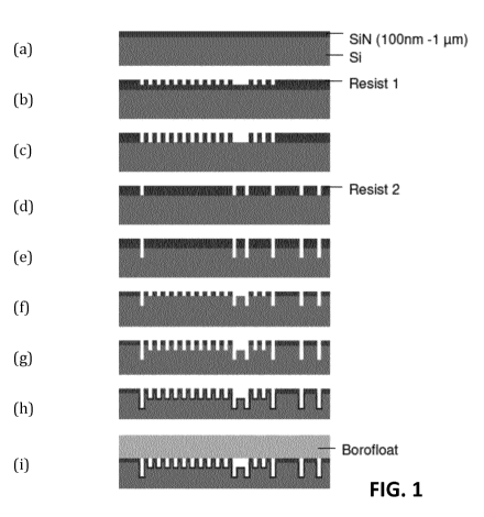
FIG. 1 illustrates a schematic overview of various steps in the production
process, such as can be used in a production method according to an embodiment
of
the present invention.
FIG. 2 illustrates a flow chart of a production process according to an
embodiment of the present invention.
FIG. 3 illustrates an anodisation setup as can be used in a production process
according to an embodiment of the present invention.
FIG. 4 illustrates an oven for a thermal treatment such as can be used in a
production process according to an embodiment of the present invention.
FIG. 5 illustrates a liquid chromatography assay according to an embodiment of
the present invention.
FIG. 6 illustrates peptides as used in an experiment, illustrating features of
embodiments of the present invention.
FIG. 7 illustrates chromatography results illustrating advantages of
embodiments of the present invention.
The drawings are only schematic and are non-limiting. In the drawings, the
size
of some of the elements may be exaggerated and not drawn on scale for
illustrative
purposes. The dimensions and the relative dimensions do not necessarily
correspond
to actual reductions of the practical embodiments of the invention. Any
reference
numbers in the claims shall not be construed as limiting the scope.
CA 03074797 2020-03-04
WO 2019/043270 PCT/EP2018/073789
8
Detailed description of illustrative embodiments
Although the present invention will be described with reference to particular
embodiments and to certain drawings, the invention is not limited thereto but
only by
the claims.
It is to be noticed that the term 'having' and 'comprising', as used in the
claims,
should not be interpreted as being restricted to the means listed thereafter;
it does not
exclude other elements or steps. It is thus to be interpreted as specifying
the presence
of the stated features, integers, steps or components as referred to, but does
not
preclude the presence or addition of one or more other features, integers,
steps or
components, or groups thereof. Thus, the scope of the expression 'a device
comprising
means A and B' should not be limited to devices consisting only of components
A and
B. It means that with respect to the present invention, the only relevant
components
of the device are A and B.
Reference throughout this specification to 'one embodiment' or 'an
embodiment' means that a particular feature, structure or characteristic
described in
connection with the embodiment is included in at least one embodiment of the
present
invention. Thus, instances of the phrases 'in one embodiment' or 'in an
embodiment'
in various places throughout this specification may, but do not necessarily,
all refer to
the same embodiment. Furthermore, the particular features, structures or
characteristics may be combined in any suitable manner, as would be apparent
to a
person of ordinary skill in the art from this disclosure, in one or more
embodiments.
Similarly it should be appreciated that in the description of exemplary
embodiments of the invention, various features of the invention are sometimes
grouped together in a single embodiment, figure, or description thereof for
the
purpose of streamlining the disclosure and aiding in the understanding of one
or more
of the various inventive aspects. This method of disclosure, however, is not
to be
interpreted as reflecting an intention that the claimed invention requires
more
features than are expressly named in each claim. Rather, as the following
claims reflect,
inventive aspects lie in less than all features of a single foregoing
disclosed
CA 03074797 2020-03-04
WO 2019/043270 PCT/EP2018/073789
9
embodiment. Thus, the claims following the detailed description are hereby
expressly
incorporated into this detailed description, with each claim standing on its
own as a
separate embodiment of this invention.
Furthermore, while some embodiments described herein include some but not
other features included in other embodiments, combinations of features of
different
embodiments are meant to be within the scope of the invention, and form
different
embodiments, as would be understood by those who are skilled in the art. For
example,
in the following claims, any of the claimed embodiments can be used in any
combination.
It should be noted that the use of particular terminology when describing
certain features or aspects of the invention should not be taken to imply that
the
terminology is being re-defined herein to be restricted to include any
specific
characteristics of the features or aspects of the invention with which that
terminology
is associated.
In a first aspect, the present invention relates to a method for producing a
chemical reactor device based on a fluid flow. Such a chemical reactor may be,
but is
not limited to, a chromatographic column. Other examples of chemical reactors
that
may benefit from the present inventions are, for example, purification filters
or
trapping columns, reactors with catalysts (micro or otherwise), multi-phase
reactors,
fuel cells, electrochemical reactors, capillary electrochromatography
reactors, etc.
Embodiments according to the present invention comprise obtaining a
substrate with a fluid channel defined by a channel wall, in which an ordered
set of
silicon pillar structures is positioned in the fluid channel. The method
further comprises
electrochemically anodising at least the silicon pillar structures to make the
silicon pillar
structures porous at least to a certain depth. In addition, the method
comprises, after
anodising, thermal treatment and functionalisation of the substrate and pillar
structures to condition at least a part of the silanol groups on the substrate
and/or
pillar structures, the thermal treatment being carried out at a temperature,
with a
duration and in an atmosphere such that any silicon oxide layer formed has a
thickness
of less than 20 nm. It is thereby an advantage of the embodiments of the
present
CA 03074797 2020-03-04
WO 2019/043270 PCT/EP2018/073789
invention that good porous structures are obtained which additionally comprise
conditioned silanol groups. These characteristics are obtained by the
combination of a
selected thermal treatment and the functionalisation step.
By way of illustration, embodiments not being limited thereto, an illustrative
5 method for producing a chemical reactor device is illustrated with
reference to FIG. 1.
The method 100 comprises, in a first step, obtaining 110 of a substrate with a
fluid channel in which an ordered set of silicon pillar structures is
positioned. This step
110 typically comprises a plurality of sub-step s. By way of example, a
possible set of
sub-step s is illustrated here, although embodiments are not limited thereto.
Other sets
10 of sub-step s, as known to those skilled in the art, which also result
in a substrate having
a fluid channel in which an ordered set of silicon pillar structures is
positioned can also
be used.
In a first sub-step 112 of an illustrative set of sub-steps, a substrate is
obtained,
in the present example a silicon substrate having a silicon nitride top layer
with a
thickness of 100 nm to 1 um, as shown in FIG. 1 part (a).
In a first sub-step 114, a resist layer is applied and a pattern is created by
lithography, for example deep UV lithography, as shown in FIG. 1 part (b).
In a third sub-step 116, a first reactive ion etch is performed on the SiN
layer,
as illustrated in FIG. 1 part (c).
In a fourth sub-step 118, a second lithographic step is performed with the aid
of a second resist layer, for example using mid-UV lithography which results
in um
accuracy, followed by a further reactive ion etch on the SiN layer, as
illustrated in FIG.
1 part (d).
In a fifth sub-step 120, some structures are further etched, for example, by
means of the Bosch process, although embodiments are not limited thereto. This
is
illustrated in FIG. 1 part (e).
After this, the resist is removed in a sixth sub-step 122 as shown in FIG. 1
part
(f) and pillars are created in a seventh sub-step 124 by means of the Bosch
process, as
shown in FIG. 1 part (g). Although the Bosch process is not essential to the
invention, it
CA 03074797 2020-03-04
WO 2019/043270 PCT/EP2018/073789
11
advantageously results in steep walls, which for example produce an angle of
inclination between 89 and 91 with respect to the plane of the substrate.
In a second step 130, the method 100 also includes the electrochemical
anodisation of at least the silicon pillar structures, as shown in FIG. 1 part
(h) to make
the silicon pillar structures porous at least to a certain depth.
In some embodiments, the electrochemical anodisation comprises, for
example, mounting the substrate in the anodisation system, adding a solution
in which
anodisation takes place, and applying an electric field for anodising.
In some embodiments, the electrochemical anodisation is based on the
.. application of a voltage. The induced voltage may for example be between
0.1 V and
5 V, for example 1.2 V. For example, the voltage can be induced for a period
between
1 minute and 60 minutes, for example between 5 minutes and 20 minutes, for
example
for 10 minutes.
In some embodiments, the electrochemical anodisation is based on the
application of a current. The induced current density can be, for example,
between
0.01 mA/cm2 and 100 mA/cm2, for example between 0.1 mA/cm2 and 5 mA/cm2. For
example, the current may be applied for a period between 5 minutes and 60
minutes,
for example between 15 minutes and 45 minutes.
The solution used to anodise may, for example, comprise an acid in some
embodiments, for example, containing HF. The solution may also contain water
and a
surface tension-reducing component, such as for example ethanol or a
surfactant.
In some embodiments based on an induced current, use is made of a decreasing
current proportional to time. This results in good porosity taking into
account the
reducing diameter of the pillars during the anodising process. In one specific
example,
use can for example be made of an initial current of 90 mA which is reduced by
1 mA/min to 70 mA (i.e. in 20 minutes). In the present example, the surface
available
for anodisation is 172.9 cm2. When selecting the current intensity, the
surface area of
the substrate can be taken into account. Finally, a number of coulombs are
sent
through the system, whereby, under the right electrochemical and/or chemical
conditions, a corresponding quantity of silicon is removed. In some
embodiments, the
CA 03074797 2020-03-04
WO 2019/043270 PCT/EP2018/073789
12
amount of material being removed can be estimated by weighing before and after
the
anodisation.
FIG. 3 illustrates an anodisation system that can be used in a production
process
according to an embodiment of the present invention.
In a third and fourth step, the method further comprises thermal treatment 140
and functionalisation 150 of the substrate and pillar structures to condition
at least a
part of the silanol groups on the substrate and/or pillar structures, the
thermal
treatment being carried out at a temperature, with a duration and in an
atmosphere
such that any silicon oxide layer formed has a thickness of less than 20 nm.
The thermal
treatment may be performed prior to the functionalisation, but after the
anodisation.
FIG. 4 illustrates an oven as can be used in a thermal treatment from a
production process according to an embodiment of the present invention.
The thermal treatment can be carried out with a duration of between 4 hours
and 20 hours, for example between 10 hours and 20 hours, for example for 15
hours,
and at a temperature between 650 C and 850 C, for example at 750 C. The
thermal
treatment can be an oxidation, although embodiments are not limited thereto.
The
oxidation can be a dry oxidation. The thermal treatment may also comprise a
rapid
thermal step (as an additional step or separately). The rapid thermal step
comprises a
treatment with a duration of between 5 minutes and 30 minutes, at a
temperature
between 700 C and 900 C, for example 800 C. It can be an oxidative step,
although
embodiments are not limited thereto.
The functionalisation may comprise silanising the substrate and the pillar
structures, for example with C18 silane, although embodiments are not limited
thereto.
In a fifth step 160, moreover, the channel is closed by providing a top
substrate,
as shown in FIG. 1 part (i). In some embodiments, this can be done by
anodically
bonding a top substrate to the pillar structure and the substrate. The top
substrate may
be a glass of substrate such as a borofloat substrate.
CA 03074797 2020-03-04
WO 2019/043270 PCT/EP2018/073789
13
In a second aspect, the present invention relates to a chemical reactor device
based on a fluid flow. The chemical reactor device comprises a substrate, such
as for
example a silicon-based substrate, with a fluid channel defined by a channel
wall. The
device further comprises an ordered set of silicon pillar structures
positioned in the
fluid channel. The pillar structures are porous to a certain depth.
Furthermore, the
silanol groups on the pillars are conditioned and any oxide layer is not
thicker than
20 nm.
According to some embodiments, the pillar structures are provided with a
predetermined number of free silanol groups adapted so as to, in the chemical
reactor
in a liquid chromatography assay for a standard mixture of peptides including
Angiotensin ll with a concentration of peptides of 0.25 ppm introduced into a
mixture
of a first mobile phase A consisting of 0.05% formic acid and 99.95% water and
a second
mobile phase B consisting of 0.05% formic acid in 1/5 water and 4/5 ACN at an
injection
volume of 1 ul, with a flow rate of 1000 nl/min, and under a gradient of 1% to
50% of
mobile phase B over a period of 30 minutes, obtain an angiotensin peak in the
chromatography with a width less than 0.2 minutes.
The features of the channels, and any pillars, may correspond to those known
in the prior art. The channels may, for example, have a width between 50 um
and
250 mm, for example between 50 um and 100 mm, for example between 50 um and
100 mm, for example between 50 um and 20 mm. The channels may have a depth
between 2 um and 1 mm, for example between 2 um and the typical wafer
thickness
of a silicon wafer. The pillars may have a typical size between 100 nm and 3
mm, for
example between 100 nm and 100 um. The inter-pillar distance between the
different
pillar structures is preferably less than 10 micrometres, for example less
than 5
micrometres. The slope of the side walls of the pillar structures can make a
slope
smaller than 2 , for example smaller than 1 , such as for example smaller than
0.5 .
In some embodiments, the chemical reactor device is a stand-alone instrument
while in other embodiments the chemical reactor device is integrated as a
component
of a lab-on-chip system.
CA 03074797 2020-03-04
WO 2019/043270 PCT/EP2018/073789
14
In a further aspect, the present invention comprises a lab-on-chip system
comprising a chemical reactor device as described in the first aspect. The lab-
on-chip
system may be a chromatographic system, for example a liquid chromatography
system, although the present invention is not limited thereto.
In yet another aspect, the present invention comprises the use of a chemical
reactor device for liquid chromatography applications, such as, for example, a
high
performance liquid chromatography application.
By way of illustration, an example is shown of a liquid chromatography assay
obtained with a chemical reactor according to an embodiment of the present
invention. The assay comprises an analysis of a peptide mixture (containing
Angiotensin II) with a 0.25 ppm concentration introduced into a mixture of a
mobile
phase A and a mobile phase B. The mobile phase A consists of 0.05% formic acid
in
99.95% water. The mobile phase B consists of a mixture of 0.05% formic acid in
1/5
water and 4/5 ACN. The injection volume is 1 ul and the flow rate is 1000
nl/min. A
gradient of 1 to 50% of mobile phase B was applied over a period of 30
minutes.
Additionally, measurements were also taken for 5 minutes at a concentration of
97.5%
of phase B, as a washing step.
The results of this assay can be seen in FIG. 5. This illustrates that a
narrow
angiotensin peak can be seen with a width that is indeed less than 0.2
minutes.
Further by way of illustration, chromatographic results are shown for a sample
comprising five peptides (of which only 4 are shown). The peptides included
are Gly-
tyr (not shown), Val-Tyr-Val (1), Leucine-Enkefaline (2), Methionine-
Enkefaline (3) en
Angiotensine ll (4) and are shown in FIG. 6. FIG. 7 shows two chromatograms
for
separation of a sample. In chromatogram A, separation of the sample in a non-
oxidized
column is shown, whereas in chromatogram B, separation of the sample in an
oxidized
column is shown. For both chromatograms, two tests are shown; one whereby the
column is modified with formic acid (FA) and one whereby the column is
modified with
CA 03074797 2020-03-04
WO 2019/043270 PCT/EP2018/073789
Trifluoracetic acid (TFA). The following chromatographic conditions are
applied.
Measurements are performed for solvent A being 100% water with the modificator
added and for solvent B being a combination of 80% acetonitrile and 20% water
with
the modificator added. Gradient chromatography was performed with a variation
from
5 1% B to 50% B in 30 minutes.
The different effects of formic acid (FA) and trifluoracetic acid (TFA) for a
same column
is due to the ion-pairing behavior of TFA. TFA fences off the positive charge
(stemming
from the amino acide arginine R) on Angiotensine II. In this way, interaction
with the
deprotoned silanols is prevented. Also for the other peptides, TFA has a
positive effect
10 because it fences off the protoned amino group (specific for 'Tryptic
Digests'). TFA also
lowers the retention (a faster elution) of some peptides because it makes the
peptides
more hydrophilic when binding.