Note: Descriptions are shown in the official language in which they were submitted.
SELF-HEALING FLEXIBLE ELECTROPHORETIC DISPLAYS
BACKGROUND
[0001] Electronic devices may include displays to present information to
users. Display
thickness may affect overall thickness of electronic devices, and thinner
displays may therefore
be used to form thinner electronic devices. In addition, electronic devices
may be subject to
damage caused by drops or other unintentional handling of electronic devices.
Such damage
may include damage to displays, such as cracking, shattering, and the like.
Displays may also
affect other aspects of electronic devices. For example, lighting components
may output light
that is visible through various portions of a device housing, which may be
undesirable and
negatively impact viewability of the display.
SUMMARY
[0002] The present description discloses a self-healing display stack for
use with an
electronic reader device, the self-healing display stack comprising:
a flexible electrophoretic display (EPD) layer comprising:
a hot melt protective sheet layer comprising a polymer substrate layer and an
optically clear adhesive layer;
an electrode layer coupled to the hot melt protective sheet layer;
a microcapsule layer coupled to the electrode layer, wherein the electrode
layer
is configured to apply a voltage to the microcapsule layer;
a flexible polyimide thin film transistor (TFT) layer coupled to the
microcapsule
layer; and
a back protective sheet coupled to the polyimide TFT layer, the back
protective
sheet configured to support the EPD layer;
a first acrylic adhesive layer coupled to the EPD layer;
a light guide coupled to the first acrylic adhesive layer;
a second acrylic adhesive layer disposed on the light guide;
a touch sensor layer coupled to the second acrylic adhesive layer;
a third acrylic adhesive layer disposed on the touch sensor layer; and
a self-healing plastic cover lens having a first surface and a second surface,
the first
surface comprising anti-glare surface features, wherein the self-healing
plastic cover
1
Date Re9ue/Date Received 2021-09-17
lens comprises a synthetic polyurethane polymer, and wherein the third acrylic
adhesive layer is in contact with the second surface.
[0002a] The present description also discloses a self-healing display
stack comprising:
a light guide configured to direct light from one or more light emitting
diodes (LEDs);
a self-healing plastic cover lens comprising a synthetic polymer and having a
first
surface comprising anti-glare features; and
a flexible electrophoretic display (EPD) comprising:
a flexible plastic thin film transistor (TFT) backplane having a first width;
an electrophoretic layer coupled to the flexible plastic TFT backplane;
an electrode layer coupled to the electrophoretic layer;
an integrated circuit disposed on the flexible plastic TFT backplane; and
a first protective sheet having a second width that is greater than or equal
to
the first width.
10002b] The present description also discloses a device comprising:
a housing; and
a self-healing display stack adhered to the housing, the self-healing display
stack
comprising:
a flexible plastic thin film transistor (TFT) backplane having a first width;
an integrated circuit disposed on the flexible plastic TFT backplane;
an electrophoretic layer coupled to the flexible TFT backplane;
an electrode layer coupled to the electrophoretic layer;
a light guide;
a self-healing plastic cover lens comprising an ultraviolet light blocking
material and a synthetic polymer, the self-healing plastic cover lens having a
first
surface comprising anti-glare features; and
a first protective sheet having a second width that is greater than or equal
to
the first width.
BRIEF DESCRIPTION OF THE DRAWINGS
[0003] FIG. 1 is a schematic illustration of a top view and cross-sectional
views of an
electronic device with a display stack in accordance with one or more
embodiments of the
disclosure.
[0004] FIGS. 2-3 are schematic illustrations of cross-sectional views of
flexible
electrophoretic display stacks in accordance with one or more embodiments of
the disclosure.
la
Date Re9ue/Date Received 2021-09-17
[0005] FIG. 4 is a schematic illustration of a cross-sectional view of a
portion of a display
stack with an integrated circuit in accordance with one or more embodiments of
the disclosure.
[0006] FIG. 5 is a schematic illustration of a self-healing flexible
electrophoretic display
stack in accordance with one or more embodiments of the disclosure.
[0007] FIG. 6 is a schematic illustration of components of a self-healing
flexible
electrophoretic display stack in accordance with one or more embodiments of
the disclosure.
[0008] FIGS. 7-8 are schematic illustrations of cross-sectional side
views of an electronic
device with a self-healing flexible electrophoretic display in accordance with
one or more
embodiments of the disclosure.
lb
Date Re9ue/Date Received 2021-09-17
CA 03074841 2020-03-04
WO 2019/055398
PCT/US2018/050429
100091 FIG. 9
is a schematic illustration of a self-healing flexible electrophoretic display
stack positioned in an electronic device in accordance with one or more
embodiments of the
disclosure.
100101 FIG. 10
is an example schematic process flow for manufacturing a protective
sheet in accordance with one or more embodiments of the disclosure.
100111 FIGS. 11-
13 are schematic illustrations of cross-sectional views of white mask
stacks in accordance with one or more embodiments of the disclosure.
100121 FIG. 14
schematically illustrates an example architecture of an electronic device
in accordance with one or more embodiments of the disclosure.
100131 The detailed description is set forth with reference to the
accompanying drawings.
The drawings are provided for purposes of illustration only and merely depict
example
embodiments of the disclosure. The drawings are provided to facilitate
understanding of the
disclosure and shall not be deemed to limit the breadth, scope, or
applicability of the
disclosure. The use of the same reference numerals indicates similar, but not
necessarily the
same or identical components. Different reference numerals may be used to
identify similar
components. Various embodiments may utilize elements or components other than
those
illustrated in the drawings, and some elements and/or components may not be
present in
various embodiments. The use of singular terminology to describe a component
or element
may, depending on the context, encompass a plural number of such components or
elements
and vice versa.
DETAILED DESCRIPTION
OVERVIEW
100141
Multimedia devices may be used to output digital content, and in some
instances,
to cause content to be presented at one or more display devices for
consumption by users. For
example, multimedia devices may be content streaming devices that stream
digital content,
and may be configured to read one or more data storage devices to cause
presentation of
content stored on the data storage device. Multimedia devices may include a
variety of
devices, such as electronic reader ("e-reader") devices, desktop computers,
portable
computers, smartphones, tablet computers, televisions, wearable devices,
speaker devices,
and so forth that may be used to access various forms of content and other
information. Such
devices may include displays that are used to present information or content
to users.
100151 Certain
electronic devices may be subject to potential damage, such as tablets or
smartphones that are susceptible to falls or drops. Resulting damage from
incidents like falls
2
CA 03074841 2020-03-04
WO 2019/055398
PCT/US2018/050429
or drops can include damage to displays, such as cracked or shattered screens.
Embodiments
of the disclosure include self-healing displays that are resistant to damage,
and may be
resistant to cracks and/or shatterproof Certain embodiments include flexible
display stacks
that have increased flexibility, thereby increasing durability of the
electronic device and/or
display. In addition, some embodiments may include relatively thinner displays
as a result of
using plastic materials instead of glass, which may facilitate thinner device
profiles. Thinner
device profiles may increase portability and/or functionality of devices by
creating additional
room for other components. Furthermore, certain devices may have light leakage
issues about
a display of the device, where light may cause issues such as a glow around an
active display,
leakage of visible light at edges of a device, and/or a halo effect about a
perimeter of a
display surface of the device. Light leakage issues may be exacerbated by a
color of a device
housing. For example, devices with white colored, or relatively lighter
colored, housings may
be more susceptible to light leakage issues than, for example, devices with
darker or black
colored housings.
100161 Embodiments of the disclosure include self-healing flexible
electrophoretic
displays. Display stacks of the disclosure may be thinner than other displays,
and may be
more durable and/or resistant to damage than other displays. Electronic
devices that include
display stacks of the disclosure may have thinner profiles, increased
functionality as a result
of increased internal space, and may avoid light leakage issues that may
negatively impact
viewability or readability of a display. In some example embodiments, the
display stacks
described herein may be flat and/or planar display stacks, while in other
example
embodiments, one or more components of the display stacks may be curved or
partially
curved. Certain embodiments of the disclosure may be aesthetically pleasing to
users by
removing light leakage and/or halo effects caused by lighting issues of
electronic devices
and/or displays.
100171 The
techniques, methods, and processes described herein may be used to
manufacture plastic-based display stack components that can replace glass-
based
components. As a result, device and display durability may be improved, and
securing or
mounting mechanisms for mounting display stacks in device housings may be
simplified. In
addition, components used to secure glass-based display components may no
longer be
needed. While described in the context of electrophoretic displays and display
stacks, aspects
of this disclosure are more broadly applicable to other forms of display
stacks and/or
displays.
3
CA 03074841 2020-03-04
WO 2019/055398
PCT/US2018/050429
100181 This
disclosure relates to, among other things, systems, methods, computer-
readable media, techniques, and methodologies for self-healing flexible
electrophoretic
displays. Display stacks, as described herein, may be used to form shatter
resistant or
shatterproof electronic displays that are relatively thin compared to other
displays, and avoid
light leakage issues regarding of device housing colors.
100191
Referring to FIG. 1, an example electronic device 100 with a display stack 110
is
depicted in accordance with one or more embodiments of the disclosure. The
display stack
110 may be a self-healing display stack for use with an electronic reader
device or other
display device. The electronic device 100 may include a housing 102 within
which a portion
of or the entire display stack 110 may be positioned. In some embodiments, the
display stack
110 may form some or all of the device housing, such as a portion of the outer
display layer.
The device 100 may be an e-reader device, a computer display, a portable
computer, a
smartphone, a tablet computer, a game console, a television, an in-vehicle
display, and so
forth. The display stack 110 may form a display of the electronic device 100
and may be
configured to present information to and/or receive inputs from a user of the
electronic device
100. In one example, the display stack 110 may form a touchscreen of the
electronic device
100, where a user may touch or press a portion of the display stack 110 to
make a selection or
another input. The device 100 may include one or more circuits, such as a
driver integrated
circuit 112, a flexible printed circuit 114, and other circuitry.
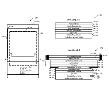
100201 A portion 120 of the display stack 110 is illustrated in cross-
sectional view along
line A-A. In the illustrated embodiment, the display stack 110 may include a
number of
layers. The layers may have different thicknesses and may not be illustrated
to scale, and may
not be illustrated to scale with respect to other layers or other figures.
100211 In FIG.
1, the portion 120 of the display stack 110 may include a protective sheet
122. The display stack 110 may include a self-healing protective sheet 122 or
plastic cover
lens 144 having a first surface and a second surface, with an anti-glare
material layer 142
disposed on the first surface. In some embodiments, the anti-glare material
and the self-
healing material layer may form a single layer. The self-healing protective
sheet 122 may be
formed of a self-healing material. Self-healing materials may be synthetic
polymers, which
have a capability to spontaneously repair damage by themselves without
external human
intervention. In some instances, cover lens surfaces can be scratched or
cracked over time,
which may affect display visibility and negatively impact a user experience.
Self-healing
materials can repair themselves through physical or chemical repairing
mechanisms that
respond to damage. Self-healing materials can include films or coatings that
can be used as
4
CA 03074841 2020-03-04
WO 2019/055398
PCT/US2018/050429
cover lens materials. Self-healing films can be free-standing films, or a
layer of coating on a
supportive substrate, such as a plastic substrate (e.g., PC, PMMA, PET, etc.).
Example self-
healing polymers include types of polyurethane or silicone, among others.
After incurring
damage, the polymer chains can reflow under room temperature and recover the
original form
factor. Such self-healing materials may have low glass transition
temperatures, such as less
than 50 C or 40 C. Certain self-healing films or coatings can be optically
clear or may have
anti-glare surface features.
100221 The
protective sheet 122 may be a front protective sheet. The protective sheet 122
may form an outer surface of the display stack 110, and in some instances, may
form an outer
surface of the device 100. The protective sheet 122 may protect the display
stack 110 from
scratches, scuffs, and other damage. In some embodiments, the protective sheet
122 may be a
multi-layered structure or composite, and may include one or more self-healing
material
layers or coatings. For example, the protective sheet 122 may include a self-
healing anti-glare
and/or anti-reflective coating disposed on a rigid substrate, such as a
plastic substrate. The
self-healing anti-glare and/or anti-reflective coating may form an outer layer
of the display
stack 110. Self-healing materials may include various polymers or plastics
with self-healing
properties, such as polyvinylidene fluoride cohexafluoropropylene, ionic
salts, and the like.
100231 A first
optically clear adhesive layer 124 may be positioned at least partially
between the protective sheet 122 and a touch sensor laver 126, and may couple
the touch
sensor layer 126 to the protective sheet 122. The first optically clear
adhesive layer 124 may
be formed of an optically clear adhesive, and may be in liquid or solid form.
In some
embodiments, the optically clear adhesive may be an adhesive tape. In some
embodiments,
the optically clear adhesive may be an acrylic adhesive.
100241 The
touch sensor layer 126 may include one or more capacitive or other touch
sensors and may be formed, at least partially, of indium tin oxide and/or a
uniform
transparent electrode.
100251 A second
optically clear adhesive layer 128 may be positioned between the touch
sensor layer 126 and a light guide 130, and may couple the light guide 130 to
the touch
sensor layer 126. The light guide 130 may be configured to direct light from
one or more
.. light emitting diodes (LEDs) or other light sources across some or all of
the display stack
110. The light guide 130 may be formed of plastic or another material. For
example, the light
guide 130 may be used to illuminate the display stack 110 in a dark
environment, and may
provide light that does not directly impinge on a viewer's eyes, so as to
reduce eye strain.
5
CA 03074841 2020-03-04
WO 2019/055398
PCT/US2018/050429
100261 A third
optically clear adhesive layer 132 may be positioned between the light
guide 130 and a flexible electrophoretic display 134, and may couple the
flexible
electrophoretic display 134 to the light guide 130. Each of the optically
clear adhesive layers
may be formed of the same or different materials or adhesives. The flexible
electrophoretic
display 134 may be an electronic ink ("e-ink") layer may include a number of
different
layers, as illustrated in example embodiments in subsequent figures. Some
embodiments may
include an electrode layer, a touch layer, a microcapsule layer, a thin film
transistor (TFT)
layer, a backplane substrate or back protective sheet layer, and/or other or
different
components or layers. One or more color adjustable light emitting diodes
(LEDs) 158 may be
positioned adjacent to one or more surfaces of the light guide 130.
100271 One or
more flexible printed circuits (FPCs) may be coupled to various
components of the display stack. For example, a touch layer FPC 160 may be
coupled to a
lower side or surface of the touch sensor layer 126. The touch layer FPC 160
may be
positioned between the touch sensor layer 126 and the second optically clear
adhesive layer
128. An LED FPC 162 may be coupled to one or more of the LEDs 158 and may be
coupled
to a lower surface of the light guide 130 with an adhesive, for example. The
LED FPC 162
may be positioned between the light guide 130 and the EPD 134. An EPD FPC 164
may be
coupled to the EPD 134 and may be positioned adjacent the third optically
clear adhesive
layer 132. The EPD FPC 164 and the LED FPC 162 may both be positioned between
the light
guide 130 and the EPD 134, with the LED FPC 162 adjacent the light guide 130
and the EPD
FPC 164 adjacent the EPD 134. Other configurations may be used.
100281 The
device housing 102 may be any suitable color, such as white, black, pink,
etc.,
and may be formed from a number of different materials, such as plastic,
aluminum, etc. The
device housing color and/or material may affect light leakage issues caused by
light leaking
about portions of the display stack 110. For example, display area glow 104
may be a glow
visible next to an active area of the display stack 110, edge light leakage
106 may be visible
light that leaks through edges of a cover lens of the display stack 110 and
may be visible after
device assembly, and/or halo effects 108 which may be visible light that is
reflected back into
the cover lens, and may appear as a narrow glow around the edges of the cover
lens of the
display stack 110, etc. Embodiments of the disclosure may mitigate one or more
light leakage
issues regardless of the device housing color and/or material.
100291 A
portion 140 of the device 100 is illustrated in cross-sectional view along
line B-
B. In the illustrated embodiment, the device 100 and/or displays stack 110 may
include a
6
CA 03074841 2020-03-04
WO 2019/055398
PCT/US2018/050429
number of layers. The layers may have different thicknesses and may not be
illustrated to
scale, and may not be illustrated to scale with respect to other layers or
other figures.
100301 The
bottom portion of the layers illustrated in portion 140 may be layers of the
display stack 110 illustrated in the portion 120. -Bottom" and -top" as used
herein are
relative and not absolute positions. For example, the flexible electrophoretic
display 134 may
form a bottom of the illustrated portion 140, and may be stacked in the
display stack with the
third optically clear adhesive layer 132, the light guide 130, the second
optically clear
adhesive layer 128, the touch sensor layer 126, the first optically clear
adhesive layer 124,
and the protective sheet 122.
100311 As illustrated in more detail in the portion 140, in some
embodiments, the
protective sheet 122 may include one or more components. For example, the
protective sheet
122 may include an anti-glare material layer 142 configured to reduce glare on
the display, a
plastic cover lens 144 configured to support the anti-glare material layer 142
and protect the
display stack 110, a low ultraviolet index material layer 146 configured to
filter ultraviolet
light, an adhesive layer 148, and a polyethylene terephthalate (PET) plastic
layer 150
configured to support one or more components and/or protect the display stack
110. The first
optically clear adhesive layer 124 may couple the protective sheet 122 to the
touch sensor
layer 126. In other embodiments, protective sheets may include additional,
fewer, or different
components. In some embodiments, certain components may not be considered to
be part of
the protective sheet and may be parts of other components or structures, such
as the plastic
cover lens. The anti-glare material layer 142 may include a self-healing
material and may
have other properties, such as ultraviolet light blocking, anti-reflective
properties, and other
properties.
100321 In
certain devices, such as devices with white colored housings, one or more
dried
ink layers may be coupled to the display stack 110 and/or another component,
so as to
mitigate light leakage issues. For example, in FIG. 1, a set of dried white
ink layers 152 may
be coupled to a surface of the PET layer 150. The dried white ink layers 152
may have a first
width and may have multiple layers. For example, the dried white ink layers
152 may include
three to five layers. The dried white ink layers 152 may be in a stacked
configuration, and
may be stacked vertically on top of each other, or may be slightly offset. A
set of dried black
ink layers 154 may be coupled to the dried white ink layers 152. The dried
black ink layers
154 may be positioned opposite the PET layer 150. The dried black ink layers
154 may have
a second width that is less than the first width, such that the dried black
ink layers 154 are not
visible from a top of the display stack 110. The number of dried black ink
layers 154 may be
7
CA 03074841 2020-03-04
WO 2019/055398
PCT/US2018/050429
less than the number of dried white ink layers 152. For example, there may be
two dried
black ink layers 154 and five dried white ink layers 152. The dried black ink
layers 154 may
be in a stacked configuration, and may be stacked vertically on top of each
other, or may be
slightly offset. The dried ink layers 152, 154 may be positioned along some or
all edges or a
perimeter of the device 100 and/or display stack 110. The dried ink layers
152, 154 may
mitigate light leakage that causes halo effects and/or display area glow.
100331 A black
edge ink layer 156 may be formed about edges of the plastic cover lens
144, and may prevent light leakage that causes edge light leakage in certain
colored devices.
The black edge ink layer 156 may be formed of the same or different ink or
material than the
dried black ink layers 154.
100341 As a
result, by using plastic components instead of glass or other materials, and
by
allowing for self-healing functionality, devices may be thinner as a result of
thinner display
stacks. Light leakage issues may be resolved or mitigated by the display
stacks and structure
of the disclosure.
100351 Example embodiments of the disclosure provide a number of technical
features or
technical effects. For example, in accordance with example embodiments of the
disclosure,
certain embodiments of the disclosure may mitigate light leakage issues,
reduce display stack
thickness, reduce device thickness, and improve durability. The above examples
of technical
features and/or technical effects of example embodiments of the disclosure are
merely
illustrative and not exhaustive.
100361 One or
more illustrative embodiments of the disclosure have been described
above. The above-described embodiments are merely illustrative of the scope of
this
disclosure and are not intended to be limiting in any way. Accordingly,
variations,
modifications, and equivalents of the embodiments disclosed herein are also
within the scope
of this disclosure. The above-described embodiments and additional and/or
alternative
embodiments of the disclosure will be described in detail hereinafter through
reference to the
accompanying drawings.
ILLUSTRATIVE EMBODIMENTS AND USE CASES
100371 FIG. 2 is a schematic illustration of a cross-sectional view of a
flexible
electrophoretic display stack 200 in accordance with one or more embodiments
of the
disclosure. The flexible electrophoretic display stack 200 may be a thin
protective sheet
flexible electrophoretic display stack. The flexible electrophoretic display
stack 200 may
include a thin protective front sheet 202 adhered or otherwise coupled to a
front plane
8
CA 03074841 2020-03-04
WO 2019/055398
PCT/US2018/050429
laminate 204 with an optically clear adhesive. Specifically, an optically
clear adhesive layer
206 may be disposed between the thin protective front sheet 202 and the front
plane laminate
204. The thin protective front sheet 202 may have a thickness of about 100
microns, the
optically clear adhesive layer 206 may have a thickness of about 175 microns,
and the front
plane laminate 204 may have a thickness of about 175 microns. In some
embodiments, an
epoxy edge seal may be disposed about a perimeter of the protective sheet 202
to increase
water resistance and/or durability. Other embodiments may include different
edge seal
materials, such as acrylic materials, ultraviolet light curable materials,
moisture barrier
materials, and other suitable materials.
100381 The flexible electrophoretic display stack 200 may include a
polyimide film laver
208. The polyimide film layer 208 may include a polymer disposed on a
substrate, and may
include imide monomers. In some embodiments, the polyimide film layer 208 may
have a
thickness of about 40 microns. In some embodiments, the front protective sheet
202 may
have a width that is greater than or equal to a width of the polyimide
backplane or polyimide
layer 208.
100391 An
optional back protective sheet 210 may support the polyimide film layer 208
and/or other components of the flexible electrophoretic display stack 200. The
back
protective sheet 210 may have a thickness of about 100 microns, and may
optionally include
an optically clear adhesive layer having a thickness of about 50 microns, for
a total thickness
of about 150 microns in one embodiment. The flexible electrophoretic display
stack 200 may
be mounted to or otherwise coupled to a mid-frame 212 of a device or housing.
In some
embodiments, the polyimide film layer 208 may be a flexible polyimide TFT
layer. The
polyimide TFT layer may be coupled to a microcapsule layer, and a back
protective sheet
may be coupled to an opposite side of the polyimide TFT layer, so as to
support the
.. polyimide TFT layer and/or the e-ink display layer.
100401 An
integrated circuit 214 may be coupled to the polyimide film layer 208. The
integrated circuit 214 may be positioned adjacent to the front plane laminate
204. To protect
the integrated circuit 214 and to stabilize and/or support the integrated
circuit and the
polyimide film layer 208, one or more portions of a sealant 216, such as a
rigid sealant, may
be positioned along one or more edges or edge surfaces of the integrated
circuit 214. The
sealant 216 may cure into a rigid material and may provide waterproofing or
water resistant
characteristics to protect the integrated circuit 214. In some embodiments, a
first rigid sealant
material may be disposed on the flexible polyimide TFT layer or polyimide film
layer 208
along a first side of the integrated circuit 214, the first rigid sealant
material configured to
9
CA 03074841 2020-03-04
WO 2019/055398
PCT/US2018/050429
support the integrated circuit 214. A second rigid sealant material may be
disposed on the
flexible polyimide TFT layer or polyimide film layer 208 along a second side
of the
integrated circuit 214 opposite the first side.
100411 A
flexible printed circuit 218 may be at least partially coupled to the
polyimide
film layer 208 and/or the integrated circuit 214. The flexible printed circuit
218 may be
supported by an ultraviolet light blocking and/or first stiffener material
220, so as to support
positioning of the flexible printed circuit 218. The first stiffener material
220 may be
positioned adjacent to the polyimide film layer 208 and may overhang an edge
of the back
protective sheet 210 by, in one example, about 1.2 mm.
100421 A similar ultraviolet light blocking and/or second stiffener
material 222, or a rigid
sealant material, may be positioned on the polyimide film layer 208 on an
opposite side of the
front plane laminate 204. The second stiffener material 222 may have a
thickness equal to or
less than, or greater than, the thickness of the optically clear adhesive
layer 206 and the front
plane laminate 204 combined. The second stiffener material 222 may increase a
water
resistance of the flexible electrophoretic display stack 200.
100431 A
similar ultraviolet light blocking and/or third stiffener material 224, or a
rigid
sealant material, may be positioned on the flexible printed circuit 218 on an
opposite side of
the optically clear adhesive layer 206. The third stiffener material 224 may
have a thickness
equal to or less than, or greater than, the thickness of the optically clear
adhesive layer 206
and the front protective sheet 202 combined. The third stiffener material 224
may increase a
water resistance of the flexible electrophoretic display stack 200.
100441 A light
blocking material 226, such as a black tape segment or other light blocking
material, may be positioned or disposed on the thin front protective sheet 202
and vertically
aligned with, or aligned with, the integrated circuit 214. The light blocking
material 226 may
prevent light from impinging on the integrated circuit 214. In some
embodiments, the
integrated circuit may be disposed adjacent to the electrophoretic layer, and
a light blocking
material layer, such as a black tape or dark tape may be positioned between
the integrated
circuit and the (hot melt) protective sheet.
100451 FIG. 3
depicts another embodiment of a flexible electrophoretic display stack 230
in accordance with one or more embodiments of the disclosure. The flexible
electrophoretic
display stack 230 may be different than the flexible electrophoretic display
stack 200 and
may include some of the same components. The flexible electrophoretic display
stack 230
may be a hot melt protective sheet flexible electrophoretic display stack.
CA 03074841 2020-03-04
WO 2019/055398
PCT/US2018/050429
100461 In the
flexible electrophoretic display stack 230, the polyimide film layer 208 may
be coupled to the optional back protective sheet 210 (which may include an
optically clear
adhesive layer). The back protective sheet 210 may be coupled to a mid-frame
component
232 that may be thicker than the mid-frame 212 of the flexible electrophoretic
display stack
200. The mid-frame 232 of the flexible electrophoretic display stack 230 may
have a
thickness of about 250 microns and may include an optional optically clear
adhesive layer
with a thickness of about 50 microns.
100471 The
first stiffener material 220 may support the flexible printed circuit 218, but
may not overhang the back protective sheet by the same amount. The light
blocking material
226 may be coupled to a surface of the integrated circuit 214, as opposed to
being disposed
on the front protective sheet in the flexible electrophoretic display stack
200. Sealant 234
may be used like the sealant 216 to support the integrated circuit 214, but a
reduced amount
may be used in the flexible electrophoretic display stack 230.
100481 A hot
melt protective sheet 236 may be disposed over the front plane laminate
204, the integrated circuit 214 and/or light blocking material 226, and a
portion of the flexible
printed circuit 218. The hot melt protective sheet 236 may conform to the
components of the
flexible electrophoretic display stack 230 and may be applied in a liquid or
semi-liquid form
in some embodiments. The hot melt protective sheet 236 may have a thickness of
about 50
microns and may provide a moisture barrier, ultraviolet light blocking, and
oxygen
penetration prevention properties. The hot melt protective sheet may be
laminated to an
electrode layer and may conform to the integrated circuit 214. The flexible
electrophoretic
display stack 230 may have an overall thickness that is less than the flexible
electrophoretic
display stack 200. In some embodiments, the hot melt protective sheet 236 may
be a
composite hot melt protective sheet layer having a polymer substrate layer and
an optically
clear adhesive layer. An electrode layer (which may be part of a front plane
laminate layer, in
an example) may be coupled to the composite hot melt protective sheet layer. A
microcapsule
layer or e-ink material layer may be coupled to the electrode layer, and the
electrode layer
may be configured to apply a voltage to the microcapsule layer, so as to
present content on
the display.
100491 In some embodiments, a flexible electrophoretic display may include
a flexible
plastic TFT backplane (e.g., polyimide backplane, etc.) having a first width.
An
electrophoretic layer may be coupled to the flexible TFT backplane, and an
electrode layer
may be coupled to the electrophoretic layer. The electrophoretic layer may be
a microcapsule
layer and may be part of a front plane laminate structure. An integrated
circuit may be
11
CA 03074841 2020-03-04
WO 2019/055398
PCT/US2018/050429
disposed on the flexible plastic TFT backplane, and a protective sheet having
a second width
that is greater than or equal to the first width. The protective sheet may be
disposed about a
side of the flexible electrophoretic display opposite the flexible TFT
backplane. The flexible
plastic TFT backplane may be formed of a polyimide material.
100501 FIG. 4 depicts a portion of a display stack 300 with an integrated
circuit 310 in
accordance with one or more embodiments of the disclosure. The integrated
circuit 310 may
be a driver integrated circuit and may drive one or more electrodes of a
display stack. The
display stack 300 may include a front plane laminate 320 and other components.
The front
plane laminate 320 may be coupled to a polyimide material layer. The
integrated circuit 310
may be disposed on the polyimide material laver adjacent to, but separated
from, the front
plane laminate 320. The integrated circuit 320 may be bonded to the polyimide
material layer
or another component of the display stack 300 with anisotropic conductive film
(ACF). ACF
bonding may include creating electric conductive adhesive bonds between
flexible and rigid
components, and may have a thickness of about 30 microns or less. For example,
a first ACF
bond 340 may be formed on a first side of the integrated circuit 310, and a
second ACF bond
350 may be formed on a second side of the integrated circuit 310. In some
embodiments, the
ACF bonds 340, 350 may bond the integrated circuit 310 to a flexible printed
circuit. An
epoxy layer 360 may be positioned about the integrated circuit 310 and may
conform to the
integrated circuit 310 and the ACF bonds 340, 350, and may be formed of an
epoxy material.
The epoxy layer 360 may be used to planarize or form a smooth surface over the
integrated
circuit 310.
100511 FIG. 5
depicts a self-healing flexible electrophoretic display stack 400 in
accordance with one or more embodiments of the disclosure. Some or all
components or
layers may not be included in other embodiments. Different embodiments may
include
additional or fewer, or different, materials, components, or layers. The
display stack 400 may
include an anti-glare and/or anti-reflective material layer 402. The anti-
glare and/or anti-
reflective material layer 402 may include one or more self-healing material
layers. In some
embodiments, the anti-glare and/or anti-reflective material layer 402 may be a
composite
layer. For example, as illustrated in FIG. 5, the anti-glare and/or anti-
reflective material layer
402 may include a self-healing material layer 404 disposed on a rigid
substrate layer 406. The
self-healing material layer 404 may have one or more anti-glare or anti-
reflective properties.
100521 A
plastic cover lens 410 may be coupled to the anti-glare and/or anti-reflective
material layer 402. The plastic cover lens 410, in one embodiment, may be a
composite layer.
For example, the plastic cover lens 410 may include an optional self-healing
material layer
12
CA 03074841 2020-03-04
WO 2019/055398
PCT/US2018/050429
412 (e.g., in some embodiments, there may not be a separate anti-glare and/or
anti-reflective
material layer 402, etc.) that is disposed on a tri-layered substrate. The tri-
layered substrate
may include a first polymethyl methacrylate (PMMA) layer 414, a second PMMA
layer 418,
and a polycarbonate layer 416 disposed between the first PMMA layer 414 and
the second
PMMA layer 418. The polycarbonate layer 416 may form a core of the tri-layered
substrate.
100531 A first
optically clear adhesive layer 420 may be disposed between the plastic
cover lens 410 and a touch layer 430. The first optically clear adhesive layer
420 may couple
the plastic cover lens 410 to the touch layer 430. The touch layer 430 may be
an olefin or
other material layer and may be used to detect capacitive or resistive touches
or contact with
the display stack. In some embodiments, the plastic cover lens may be a
composite self-
healing plastic cover lens with a rigid plastic substrate layer, and a self-
healing material layer
disposed on the rigid plastic substrate layer. The self-healing material layer
may be
positioned between the rigid plastic substrate layer and the anti-glare
material layer. In some
embodiments, the self-healing plastic cover lens may be a composite self-
healing plastic
cover lens having a plastic substrate layer, an anti-glare material layer, and
a self-healing
material layer disposed on the plastic substrate layer. The self-healing
material layer may be
positioned between the plastic substrate layer and the anti-glare material
layer, or may form
an outer surface of the structure. The self-healing material layer may serve,
in some
embodiments, as an anti-glare material. For example, some self-healing
materials can be hot-
.. embossed to form surface structures or surface features that have anti-
glare properties.
Example surface features may include roughening features that scatter light
and reduce glare
without affecting transparency, such as teeth or other textured surfaces like
lotus leafs and
other patterns. The self-healing material may be the first layer on the cover
lens that users can
interact with. In some embodiments, the plastic cover lens may not include a
self-healing
material or have self-healing properties. In other embodiments, the plastic
cover lens may
include an ultraviolet light blocking material, such as an ultraviolet light
blocking coating, a
UV-cut material, or another UV-protective material. The UV protective material
may be a
layer of the plastic cover lens, or may be integrated into a layer of the
plastic cover lens, and
may protect the plastic components of the display stack from a yellowing
effect as a result of
.. exposure to ultraviolet light. The UV protective material may have various
UV light blocking
properties. For example, the UV protective material may allow 2.3% of
ultraviolet light
having a wavelength of about 360nm to about 370nm to penetrate the UV
protective material.
In other words, the UV protective material may have a transparency of about
2.3% for
wavelengths 360nm-370nm, a transparency of about 10% for wavelengths 370nm-
380nm, a
13
CA 03074841 2020-03-04
WO 2019/055398
PCT/US2018/050429
transparency of about 300/a for wavelengths 380nm-390nm, and/or a transparency
of about
75% for wavelengths equal to or greater than about 440nm. Other embodiments
may have
different UV related values.
100541 A second
optically clear adhesive layer 440 may be disposed between the touch
layer 430 and a light guide 450. A third optically clear adhesive layer 460
may be disposed
between the light guide 450 and a flexible electrophoretic display layer 470.
In some
embodiments, the touch sensor layer may be integrated into the light guide.
For example, the
touch sensor layer may be at least partially formed by optical patterning on a
surface of the
light guide 450. In other embodiments, the touch sensor layer may be
integrated into a
"bottom" or lower surface of the plastic cover lens 410.
100551 The
flexible electrophoretic display layer 470 may include a number of flexible
electrophoretic display embodiments. For example, in FIG. 5, the flexible
electrophoretic
display layer 470 may include a hot melt protective sheet 472. In some
embodiments, the hot
melt protective sheet 472 may be a composite sheet and may include a composite
polymer
.. 474 (which may be formed of a self-healing material) disposed on an
optically clear adhesive
layer 476. Other embodiments may include different types of hot melt
protective sheets with
different properties.
100561 The hot
melt protective sheet 472 may be positioned adjacent to a PET indium tin
oxide electrode layer 480, which may facilitate touch detection for the
display stack 400. The
PET indium tin oxide electrode layer 480 may be coupled to a microcapsule
layer 482, which
may be an e-ink layer with a number of polyurethane or other microcapsules
configured to
react to an electrode or electric charge. The microcapsule layer 482 may
include a dielectric
solvent (e.g., a high dielectric, low viscosity suspending medium) and charged
particles
dispersed throughout the dielectric solvent. The charged particles may be of
different colors
(e.g., a combination of white, black, and/or colored particles). White
particles and color
particles, or white particles and black particles, may move within the
dielectric solvent in
response to an electric field applied thereto. For a mono type display stack,
which generates
black and white images on the display, the microcapsule layer 482 may contain
white and
black particles. For a display stack configured to generate colored images,
the microcapsule
layer 482 may contain white and colored particles. In some embodiments, the
microcapsule
layer 482 may have a thickness that is no greater than about 400 microns, no
greater than
about 350 microns, no greater than about 300 microns, no greater than about
300 microns, no
greater than about 250 microns. no greater than about 200 microns, no greater
than about 150
14
CA 03074841 2020-03-04
WO 2019/055398
PCT/US2018/050429
microns, no greater than about 120 microns, no greater than about 100 microns,
no greater
than about 80 microns, or no greater than about 60 microns.
100571 The PET
indium tin oxide electrode layer 480 may be coupled to a polyimide TFT
layer 484. The polyimide TFT layer 484 may define an active area with one or
more
transistors. The polyimide TFT layer 484 may be configured to provide an
electric field to
influence the movement of charged particles within the microcapsule layer 482,
which, in
turn, may cause an image to be formed on the display. That is, if an
electrical signal is
applied to an electrode on the surface of the polyimide TFT layer 484, an
electric field may
be generated between the polyimide TFT layer 484 and the microcapsule layer
482. The
generated electric field may cause charged particles (e.g., white, black,
grey, and/or colored
particles) to move within the microcapsule layer 482 so that an image or other
content can be
generated on the display of the device.
100581 In
embodiments with a passive matrix display, the polyimide TFT layer 484 may
be patterned with a row electrode and a transparent conductive layer or the
microcapsule
layer 482 may include a column electrode, or vice versa. In embodiments with
an active
matrix display, the polyimide TFT layer 484 may include one or more pixel
electrode(s), and
the microcapsule layer 482 may include a uniform transparent electrode, such
as a uniform
layer of indium tin oxide. In a segmented-electrode display embodiment,
segmented
electrodes may be provided on a substrate, such as the polyimide TFT layer
484, and may
each be driven independently with the desired voltage to give the desired
optical state in a so-
called "direct drive" scheme). In such embodiments, the microcapsule layer 482
may include
a uniform transparent electrode. The polyimide TFT layer 484 may be disposed
on a
substantially flat portion or platform of the housing 102. The polyimide TFT
layer 484 may
also include a set of patterned electrodes with each electrode connected to
its own driver,
such as a segmented display.
100591 An
optional back protective sheet 486 may be coupled to, or positioned adjacent,
the polyimide TFT layer 484 or TFT backplane and may support the polyimide TFT
layer
484 and/or the display stack 400. The self-healing flexible electrophoretic
display stack 400
may be used, for example, in devices with dark colored housings or light
colored housings. A
rigid sealant material may be disposed on the back protective sheet adjacent
to at least one
edge of the flexible plastic TFT backplane in some embodiments.
100601 FIG. 6
depicts a self-healing flexible electrophoretic display stack 500 in
accordance with one or more embodiments of the disclosure. The self-healing
flexible
electrophoretic display stack 500 may include three components in the
illustrated
CA 03074841 2020-03-04
WO 2019/055398
PCT/US2018/050429
embodiment. In particular, a protective sheet 510 may be coupled to a front
plane laminate
530. The front plane laminate 530 may be coupled to a TFT backplane and driver
layer 550.
100611 The
protective sheet 510 may include an anti-reflective and/or anti-glare material
layer 512 on an outer surface of the protective sheet 510. The anti-reflective
and/or anti-glare
material layer 512 may be disposed on a PET layer 514. A soft adhesive layer
516 may be
positioned on a side of the PET layer 514 opposite the anti-reflective and/or
anti-glare
material layer 512. A barrier film layer 518 may be disposed on the soft
adhesive layer 516
and coupled to the PET layer 514. An inorganic coating 520 may be disposed on
the barrier
film layer 518.
100621 The front plane laminate 530 may be an e-ink layer and may include
one or more
microcapsules disposed between electrodes. For example, the front plane
laminate 530 may
include a top transparent electrode 532 and a bottom electrode 534. A number
of
microcapsules 536 may be disposed between the top transparent electrode 532
and the bottom
electrode 534. One or more, or each, of the microcapsules 536 may include a
positively
charged black pigment 538 and/or a negatively charged white pigment 540. The
black
pigment 538 and the white pigment 540 may be disposed or submersed in a clear
fluid 542 in
the respective microcapsules 536. In some embodiments, the microcapsules 536
may be sub-
capsule addressed to increase resolution and/or improve display capability. An
example of a
sub-capsule addressed microcapsule 544 is illustrated in FIG. 6.
100631 The TFT backplane and driver layer 550 may include gate drivers and
select/row
lines 552, and may also include source drivers and data/column lines 554. The
TFT
backplane and driver layer 550 may drive one or more components of the front
plane
laminate 530 to present content on the display stack 500.
100641 FIGS. 7-
8 depict electronic devices with self-healing flexible electrophoretic
displays in accordance with one or more embodiments of the disclosure. In FIG.
7, a device
600 may include a self-healing flexible electrophoretic display 610. The self-
healing flexible
electrophoretic display 610 may include a front protective sheet 612, a front
plane laminate
614, a polyimide material layer 616, and a back protective sheet 618.
100651 The
device 600 may include a cover lens 620 coupled to the self-healing flexible
electrophoretic display 610 with one or more optically clear adhesive layers
622. The device
600 may include a driver integrated circuit 624 and a flexible printed circuit
626. An epoxy
seal 628 may be disposed about the driver integrated circuit 624.
100661 To
support the flexible printed circuit 626 during assembly, a portion of double
sided tape 630 may be used to couple the flexible printed circuit 626 to the
cover lens 620.
16
CA 03074841 2020-03-04
WO 2019/055398
PCT/US2018/050429
The double sided tape 630 may secure the flexible printed circuit 626 and may
provide
stability during and after assembly.
100671 In FIG.
8, another embodiment of a device 650 with a self-healing flexible
electrophoretic display 660 is illustrated. In FIG. 8, the self-healing
flexible electrophoretic
display 660 may include a front protective sheet 662 coupled to a front plane
laminate 664
with one or more optically clear adhesive layers 666. The front plane laminate
664 may be
coupled to a polyimide layer 668. The polyimide layer 668 may be disposed on a
back
protective sheet 670. The back protective sheet 670 may be mounted on or
secured to a mid-
frame 672 of the device 650.
100681 A driver integrated circuit 674 may be disposed on the polyimide
layer 668
adjacent to the front plane laminate 664. One or more portions of rigid
sealant 676 may be
disposed along one or more sides or edges of the driver integrated circuit
674. Additional
sealant and/or stiffener material may include a second sealant portion 678
positioned adjacent
to the front plane laminate 664 and may be disposed on the polyimide layer
668. A third
sealant portion 680 may be disposed adjacent to the front protective sheet 662
and disposed
on a flexible printed circuit 682. A fourth sealant portion 684 or stiffener
may be disposed on
a side of the flexible printed circuit 682 opposite the third sealant portion
680. The fourth
sealant portion 684 may overhang the back protective sheet 670 by a distance
686. A portion
of double sided tape 688 may be used to couple the flexible printed circuit
682 to a cover lens
690 of the device 650. The double sided tape 688 may have a width 692 that is
greater than
the overhang distance 686.
100691 FIG. 9
depicts a self-healing flexible electrophoretic display assembly 710
positioned in an electronic device 700 in accordance with one or more
embodiments of the
disclosure. The device 700 may include a housing 702 with a grip portion 704
configured to
be held by users during operation of the device 700, and a blade portion 706,
which may be
relatively thinner than the grip portion 704. The housing 702 may be formed of
one or more
materials. For example, the housing 702 may be formed of aluminum, while
another portion
708 of the housing may be formed of plastic. A rubber ring 712 may be
positioned in the
portion 708 of the housing formed of plastic.
100701 A plastic cover lens 714 may form an outer surface of the device
700. The plastic
cover lens 714 may be coupled to the self-healing flexible electrophoretic
display assembly
710, for example, with an optically clear adhesive. The self-healing flexible
electrophoretic
display assembly 710 may be adhered to the housing 702 of the device 700 with
an adhesive
716. Because the self-healing flexible electrophoretic display assembly 710
does not include
17
CA 03074841 2020-03-04
WO 2019/055398
PCT/US2018/050429
glass, and because of the flexible and shatter resistant characteristics of
the self-healing
flexible electrophoretic display assembly 710, the self-healing flexible
electrophoretic display
assembly 710 may be mounted to the housing 702 of the device 700 with the
adhesive 716.
100711 A
battery 720 may be adhered to the housing 702 in the grip portion 704 with an
adhesive 722. An antenna assembly 724 may be positioned in the grip portion
704 adjacent to
the battery 720. An epoxy shield 728 may be disposed on the battery 720 and
may be in
contact with a flexible printed circuit 730. A page turn button assembly 732
may be disposed
adjacent the cover lens 714. An adhesive 734 may secure the cover lens 714 to
a portion of
the housing 702 or another component of the device 700.
100721 FIG. 10 is an example schematic process flow for manufacturing a
protective
sheet in accordance with one or more embodiments of the disclosure. At a first
step 750, a
polyimide film 752 is provided on a carrier glass 754. The carrier glass 754
may be coated
with the polymer. At a second step 760 the display function layers are built
on the polyimide
film 752. For example, a TFT matrix layer 756 and an electrophoretic layer 758
are coupled
to the polyimide film 752. At a third step 770, the display layers are de-
bonded from the
carrier glass 754. Al a fourth step 780, the flexible display on a polymer
film is formed
without the carrier glass. As a result of removing glass from this structure,
an assembled
weight of the structure may be reduced, and flexibility of the structure may
be increased.
Devices incorporating the structure may therefore be thinner, lighter, and
more reliable and
durable.
100731 FIGS. 11-
13 are schematic illustrations of cross-sectional views of white mask
stacks in accordance with one or more embodiments of the disclosure. The white
mask stacks
may be used for devices that have lighter colored, such as white colored,
housings, or devices
where light leakage affects usage of the device.
100741 A first embodiment 800 includes a display stack 802 where a first
optically clear
adhesive layer 804 couples the display stack 802 to a set of components, some
of which may
collectively form a cover lens for the device. In particular, the first
optically clear adhesive
layer 804 may couple the display stack 802 to a polycarbonate layer 806. A
second optically
clear adhesive layer 808 may couple the polycarbonate layer 806 to an
optically clear
planarization coating layer 810. The optically clear planarization coating
layer 810 maybe
coupled to a PET layer 812 with ultraviolet light blocking or filtering
properties. An anti-
glare coating 814 may include a self-healing material and may be coupled to
the PET layer
812.
18
CA 03074841 2020-03-04
WO 2019/055398
PCT/US2018/050429
100751 The
optically clear planarization coating layer 810 may be used to planarize a
layer of the white mask that includes one or more dried white ink layers and
one or more
dried black ink layers. For example, a set of dried white ink layers 820 may
be coupled to a
surface of the PET layer 812. The set of dried white ink layers 820 may be
disposed about a
.. perimeter of the PET layer 812. A set of dried black ink layers 822 may be
coupled to the
dried white ink layers 820. The white mask may include more dried white ink
layers 820 than
dried black ink layers 822. Other ink colors may be used, with relatively dark
colored layers
positioned "lower" in the stack than relatively lighter colored layers. Black
ink layers 824
may be disposed about edges of the white mask, so as to prevent light leakage
about edges of
.. the device housing.
100761 The PET
layer 812 may have a thickness of about 75 microns, the optically clear
planarization coating layer 810 may have a thickness of about 30-50 microns,
the second
optically clear adhesive layer 808 may have a thickness of about 100 microns,
and the
polycarbonate layer 806 may have a thickness of about 0.4 to about 0.5
millimeters. The
white mask in the first embodiment 800 may therefore have an increased
thickness of
between about 100 to about 250 microns relative to other assemblies without
white masks.
100771 In a
second embodiment 830, the display stack 802 and the first optically clear
adhesive layer 804 may be included. However, the dried white ink layers 820
and the dried
black ink layers 822 may be positioned at the first optically clear adhesive
layer 804, and a
planarization layer may not be included. The first optically clear adhesive
layer 804 may have
a thickness of about 175 microns in the second embodiment. The dried white ink
layers 820
may be coupled to a PET layer 832 having a thickness of about 50 microns. An
adhesive
layer 834 may be disposed on the PET layer 832 opposite the dried white ink
layers 820. A
low index coating layer 836 may be disposed on the adhesive layer 834 and may
have a
.. thickness of about 2 microns. The low index coating layer 836 may be a low
refraction index
material having, in an example, a refractive index value of equal to or
greater than about 1.0
and less than or equal to about 1.28, such as about 1.000293nm. The low index
coating layer
836 may be a low refraction index material with hollow spheres of glass filled
with air, where
the hollow spheres have a thickness of about 60nm. In another example, the
hollow spheres
may be silica hollow spheres in a silicone or acrylic resin layer.
100781 The
adhesive layer 834 may support the low index coating layer 836. A co-
extruded tri-layer plastic cover lens 838 may be positioned adjacent the low
index coating
layer 836. The co-extruded tri-layer plastic cover lens 838 may include a
first PMMA layer, a
polvcarbonate laver, and a second PMMA layer, where the polycarbonate layer is
disposed
19
CA 03074841 2020-03-04
WO 2019/055398
PCT/US2018/050429
between the first PMMA layer and the second PMMA layer. The anti-glare coating
814 may
be disposed on the co-extruded tri-layer plastic cover lens 838. The second
embodiment 830
may include edge ink layers 840 along edges of the co-extruded tri-layer
plastic cover lens
838, and the edge ink layers 840 may not extend vertically down the assembly,
unlike in the
first embodiment 800. The second embodiment 830 may be slightly wider than the
first
embodiment 800, and the co-extruded tri-layer plastic cover lens 838 may have
a greater
width than the display stack 802. The second embodiment 830 may have an
overall thickness
that is about 70 microns to about 120 microns thicker than other devices
without white
masks.
100791 A third
embodiment 850 may be similar to the second embodiment 830, but may
have a different arrangement and structure. For example, in the third
embodiment 850, the
display stack 802 may be coupled to the first optically clear adhesive layer
804, and the dried
white ink layers 820 and the dried black ink layers 822 may be disposed
adjacent the first
optically clear adhesive layer 804.
100801 The low index
coating layer 836 may be positioned adjacent to the first optically
clear adhesive layer 804 instead of adjacent to the co-extruded tri-layer
plastic cover lens
838. An acrylic layer 852 having a thickness of about 7 to 10 microns may be
positioned
adjacent the low index coating layer 836. An adhesive layer 854 having a
thickness of about
10 microns (as opposed to the 20 micron thickness of the adhesive layer 834 in
the second
embodiment 830) may be positioned adjacent the acrylic layer 852. The co-
extruded tri-layer
plastic cover lens 838 may be positioned adjacent to the adhesive layer 854.
The anti-glare
layer 814 may be disposed on the co-extruded tri-layer plastic cover lens 838,
and the edge
ink layers 840 may be disposed along the edge surfaces of the co-extruded tri-
layer plastic
cover lens 838.
100811 One or more
operations of the methods, process flows, or use cases of FIGS. 1-13
may have been described above as being performed by a user device, or more
specifically, by
one or more program module(s), applications, or the like executing on a
device. It should be
appreciated, however, that any of the operations of the methods, process
flows, or use cases
of FIGS. 1-13 may be performed, at least in part, in a distributed manner by
one or more
other devices, or more specifically, by one or more program module(s),
applications, or the
like executing on such devices. In addition, it should be appreciated that
processing
performed in response to the execution of computer-executable instructions
provided as part
of an application, program module. or the like may be interchangeably
described herein as
being performed by the application or the program module itself or by a device
on which the
CA 03074841 2020-03-04
WO 2019/055398
PCT/US2018/050429
application, program module, or the like is executing. While the operations of
the methods,
process flows, or use cases of FIGS. 1-13 may be described in the context of
the illustrative
devices, it should be appreciated that such operations may be implemented in
connection with
numerous other device configurations.
100821 The operations described and depicted in the illustrative methods,
process flows,
and use cases of FIGS. 1-13 may be carried out or performed in any suitable
order, such as
the depicted orders, as desired in various example embodiments of the
disclosure.
Additionally, in certain example embodiments, at least a portion of the
operations may be
carried out in parallel. Furthermore, in certain example embodiments, less,
more, or different
operations than those depicted in FIGS. 1-13 may be performed.
100831 Although
specific embodiments of the disclosure have been described, one of
ordinary skill in the art will recognize that numerous other modifications and
alternative
embodiments are within the scope of the disclosure. For example, any of the
functionality
and/or processing capabilities described with respect to a particular device
or component may
be performed by any other device or component. Further, while various
illustrative
implementations and architectures have been described in accordance with
embodiments of
the disclosure, one of ordinary skill in the art will appreciate that numerous
other
modifications to the illustrative implementations and architectures described
herein are also
within the scope of this disclosure.
100841 Certain aspects of the disclosure are described above with reference
to block and
flow diagrams of systems, methods, apparatuses, and/or computer program
products
according to example embodiments. It will be understood that one or more
blocks of the
block diagrams and flow diagrams, and combinations of blocks in the block
diagrams and the
flow diagrams, respectively, may be implemented by the execution of computer-
executable
program instructions. Likewise, some blocks of the block diagrams and flow
diagrams may
not necessarily need to be performed in the order presented, or may not
necessarily need to be
performed at all, according to some embodiments. Further, additional
components and/or
operations beyond those depicted in blocks of the block and/or flow diagrams
may be present
in certain embodiments.
100851 Accordingly, blocks of the block diagrams and flow diagrams support
combinations of means for performing the specified functions, combinations of
elements or
steps for performing the specified functions, and program instruction means
for performing
the specified functions. It will also be understood that each block of the
block diagrams and
flow diagrams, and combinations of blocks in the block diagrams and flow
diagrams, may be
21
CA 03074841 2020-03-04
WO 2019/055398
PCT/US2018/050429
implemented by special-purpose, hardware-based computer systems that perform
the
specified functions, elements or steps, or combinations of special-purpose
hardware and
computer instructions.
ILLUSTRATIVE COMPUTER ARCHITECTURE
100861 FIG. 14
is a schematic block diagram of one or more illustrative electronic
device(s) 900 in accordance with one or more example embodiments of the
disclosure. The
electronic device(s) 900 may include any suitable computing device including,
but not
limited to, a server system, a mobile device such as a smartphone, a tablet,
an e-reader, a
wearable device, or the like; a desktop computer; a laptop computer; a content
streaming
device; a set-top box; a scanning device; a barcode scanning wand; or the
like. The electronic
device(s) 900 may correspond to an illustrative device configuration for the
device(s) of
FIGS. 1-13.
100871 The
electronic device(s) 900 may be configured to communicate with one or more
servers, user devices, or the like. The electronic device(s) 900 may be
configured to
determine voice commands, determine wakeword utterances, present digital
content,
determine and/or control other devices, and other operations.
100881 The
electronic device(s) 900 may be configured to communicate via one or more
networks. Such network(s) may include, but are not limited to, any one or more
different
types of communications networks such as, for example, cable networks, public
networks
(e.g., the Internet), private networks (e.g., frame-relay networks), wireless
networks, cellular
networks, telephone networks (e.g., a public switched telephone network), or
any other
suitable private or public packet-switched or circuit-switched networks.
Further, such
network(s) may have any suitable communication range associated therewith and
may
include, for example, global networks (e.g., the Internet), metropolitan area
networks
(MANs), wide area networks (WANs), local area networks (LANs), or personal
area
networks (PANs). In addition, such network(s) may include communication links
and
associated networking devices (e.g., link-layer switches, routers, etc.) for
transmitting
network traffic over any suitable type of medium including, but not limited
to, coaxial cable,
twisted-pair wire (e.g., twisted-pair copper wire), optical fiber, a hybrid
fiber-coaxial (HFC)
medium, a microwave medium, a radio frequency communication medium, a
satellite
communication medium, or any combination thereof
100891 In an
illustrative configuration, the electronic device(s) 900 may include one or
more processors (processor(s)) 902, one or more memory devices 904 (also
referred to herein
22
CA 03074841 2020-03-04
WO 2019/055398
PCT/US2018/050429
as memory 904), one or more input/output (I/O) interface(s) 906, one or more
network
interface(s) 908, one or more sensor(s) or sensor interface(s) 910, one or
more transceiver(s)
912, one or more display stack(s) 914, one or more optional microphone(s) 916,
and data
storage 920. The electronic device(s) 900 may further include one or more
bus(es) 918 that
functionally couple various components of the electronic device(s) 900. The
electronic
device(s) 900 may further include one or more antenna(e) 926 that may include,
without
limitation, a cellular antenna for transmitting or receiving signals to/from a
cellular network
infrastructure, an antenna for transmitting or receiving Wi-Fi signals to/from
an access point
(AP), a Global Navigation Satellite System (GNSS) antenna for receiving GNSS
signals from
a GNSS satellite, a Bluetooth antenna for transmitting or receiving Bluetooth
signals, a Near
Field Communication (NFC) antenna for transmitting or receiving NFC signals,
and so forth.
These various components will be described in more detail hereinafter.
100901 The
bus(es) 918 may include at least one of a system bus, a memory bus, an
address bus, or a message bus, and may permit the exchange of information
(e.g., data
(including computer-executable code), signaling, etc.) between various
components of the
electronic device(s) 900. The bus(es) 918 may include, without limitation, a
memory bus or a
memory controller, a peripheral bus, an accelerated graphics port, and so
forth. The bus(es)
918 may be associated with any suitable bus architecture including, without
limitation, an
Industry Standard Architecture (ISA), a Micro Channel Architecture (MCA), an
Enhanced
ISA (EISA), a Video Electronics Standards Association (VESA) architecture, an
Accelerated
Graphics Port (AGP) architecture, a Peripheral Component Interconnect (PCI)
architecture, a
PCI-Express architecture, a Personal Computer Memory Card International
Association
(PCMCIA) architecture, a Universal Serial Bus (USB) architecture, and so
forth.
100911 The
memory 904 of the electronic device(s) 900 may include volatile memory
(memory that maintains its state when supplied with power) such as random
access memory
(RAM) and/or non-volatile memory (memory that maintains its state even when
not supplied
with power) such as read-only memory (ROM), flash memory, ferroelectric RAM
(FRAM),
and so forth. Persistent data storage, as that term is used herein, may
include non-volatile
memory. In certain example embodiments, volatile memory may enable faster
read/write
access than non-volatile memory. However, in certain other example
embodiments, certain
types of non-volatile memory (e.g., FRAM) may enable faster read/write access
than certain
types of volatile memory.
100921 In
various implementations, the memory 904 may include multiple different types
of memory such as various types of static random access memory (SRAM), various
types of
23
CA 03074841 2020-03-04
WO 2019/055398
PCT/US2018/050429
dynamic random access memory (DRAM), various types of unalterable ROM, and/or
writeable variants of ROM such as electrically erasable programmable read-only
memory
(EEPROM), flash memory, and so forth. The memory 904 may include main memory
as well
as various forms of cache memory such as instruction cache(s), data cache(s),
translation
lookaside buffer(s) (TLBs), and so forth. Further, cache memory such as a data
cache may be
a multi-level cache organized as a hierarchy of one or more cache levels (L1,
L2, etc.).
100931 The data
storage 920 may include removable storage and/or non-removable
storage including, but not limited to, magnetic storage, optical disk storage,
and/or tape
storage. The data storage 920 may provide non-volatile storage of computer-
executable
.. instructions and other data. The memory 904 and the data storage 920,
removable and/or non-
removable, are examples of computer-readable storage media (CRSM) as that term
is used
herein.
100941 The data
storage 920 may store computer-executable code, instructions, or the like
that may be loadable into the memory 904 and executable by the processor(s)
902 to cause
the processor(s) 902 to perform or initiate various operations. The data
storage 920 may
additionally store data that may be copied to the memory 904 for use by the
processor(s) 902
during the execution of the computer-executable instructions. Moreover, output
data
generated as a result of execution of the computer-executable instructions by
the processor(s)
902 may be stored initially in the memory 904, and may ultimately be copied to
the data
.. storage 920 for non-volatile storage.
100951 More
specifically, the data storage 920 may store one or more operating systems
(0/S) 922; one or more database management systems (DBMS) 924; and one or more
program module(s), applications, engines, computer-executable code, scripts,
or the like.
Some or all of these module(s) may be sub-module(s). Any of the components
depicted as
.. being stored in the data storage 920 may include any combination of
software, firmware,
and/or hardware. The software and/or firmware may include computer-executable
code,
instructions, or the like that may be loaded into the memory 904 for execution
by one or more
of the processor(s) 902. Any of the components depicted as being stored in the
data storage
920 may support functionality described in reference to corresponding
components named
.. earlier in this disclosure.
100961 The data
storage 920 may further store various types of data utilized by the
components of the electronic device(s) 900. Any data stored in the data
storage 920 may be
loaded into the memory 904 for use by the processor(s) 902 in executing
computer-
executable code. In addition, any data depicted as being stored in the data
storage 920 may
24
CA 03074841 2020-03-04
WO 2019/055398
PCT/US2018/050429
potentially be stored in one or more datastore(s) and may be accessed via the
DBMS 924 and
loaded in the memory 904 for use by the processor(s) 902 in executing computer-
executable
code. The datastore(s) may include, but are not limited to, databases (e.g.,
relational, object-
oriented, etc.), file systems, flat files, distributed datastores in which
data is stored on more
than one node of a computer network, peer-to-peer network datastores, or the
like.
100971 The
processor(s) 902 may be configured to access the memory 904 and execute
the computer-executable instructions loaded therein. For example, the
processor(s) 902 may
be configured to execute the computer-executable instructions of the various
program
module(s), applications, engines, or the like of the electronic device(s) 900
to cause or
facilitate various operations to be performed in accordance with one or more
embodiments of
the disclosure. The processor(s) 902 may include any suitable processing unit
capable of
accepting data as input, processing the input data in accordance with stored
computer-
executable instructions, and generating output data. The processor(s) 902 may
include any
type of suitable processing unit including, but not limited to, a central
processing unit, a
microprocessor, a Reduced Instruction Set Computer (RISC) microprocessor, a
Complex
Instruction Set Computer (CISC) microprocessor, a microcontroller, an
Application Specific
Integrated Circuit (ASIC), a Field-Programmable Gate Array (FPGA), a System-on-
a-Chip
(SoC), a digital signal processor (DSP), and so forth. Further, the
processor(s) 902 may have
any suitable microarchitecture design that includes any number of constituent
components
such as, for example, registers, multiplexers, arithmetic logic units, cache
controllers for
controlling read/write operations to cache memory, branch predictors, or the
like. The
microarchitecture design of the processor(s) 902 may be capable of supporting
any of a
variety of instruction sets.
100981
Referring now to other illustrative components depicted as being stored in the
data
storage 920, the 0/S 922 may be loaded from the data storage 920 into the
memory 904 and
may provide an interface between other application software executing on the
electronic
device(s) 900 and the hardware resources of the electronic device(s) 900. More
specifically,
the 0/S 922 may include a set of computer-executable instructions for managing
the
hardware resources of the electronic device(s) 900 and for providing common
services to
other application programs (e.g., managing memory allocation among various
application
programs). In certain example embodiments, the 0/S 922 may control execution
of the other
program module(s). The 0/S 922 may include any operating system now known or
which
may be developed in the future including, but not limited to, any server
operating system, any
mainframe operating system, or any other proprietary or non-proprietary
operating system.
CA 03074841 2020-03-04
WO 2019/055398
PCT/US2018/050429
100991 The DBMS
924 may be loaded into the memory 904 and may support
functionality for accessing, retrieving, storing, and/or manipulating data
stored in the memory
904 and/or data stored in the data storage 920. The DBMS 924 may use any of a
variety of
database models (e.g., relational model, object model, etc.) and may support
any of a variety
of query languages. The DBMS 924 may access data represented in one or more
data
schemas and stored in any suitable data repository including, but not limited
to, databases
(e.g., relational, object-oriented, etc.), file systems, flat files,
distributed datastores in which
data is stored on more than one node of a computer network, peer-to-peer
network datastores,
or the like. In those example embodiments in which the electronic device(s)
900 is a mobile
device, the DBMS 924 may be any suitable lightweight DBMS optimized for
performance on
a mobile device.
101001
Referring now to other illustrative components of the electronic device(s)
900, the
input/output (I/O) interface(s) 906 may facilitate the receipt of input
information by the
electronic device(s) 900 from one or more I/O devices as well as the output of
information
from the electronic device(s) 900 to the one or more I/O devices. The I/O
devices may
include any of a variety of components such as a display or display screen
haying a touch
surface or touchscreen; an audio output device for producing sound, such as a
speaker; an
audio capture device, such as a microphone; an image and/or video capture
device, such as a
camera; a haptic unit: and so forth. Any of these components may be integrated
into the
electronic device(s) 900 or may be separate. The I/O devices may further
include, for
example, any number of peripheral devices such as data storage devices,
printing devices, and
so forth.
101011 The I/O
interface(s) 906 may also include an interface for an external peripheral
device connection such as universal serial bus (USB), FireWire, Thunderbolt,
Ethernet port
or other connection protocol that may connect to one or more networks. The I/O
interface(s)
906 may also include a connection to one or more of the antenna(e) 926 to
connect to one or
more networks via a wireless local area network (WLAN) (such as Wi-Fi) radio,
Bluetooth,
ZigBee, and/or a wireless network radio, such as a radio capable of
communication with a
wireless communication network such as a Long Term Evolution (LTE) network,
WiMAX
network, 3G network, a ZigBee network, etc.
101021 The
electronic device(s) 900 may further include one or more network interface(s)
908 via which the electronic device(s) 900 may communicate with any of a
variety of other
systems, platforms, networks, devices, and so forth. The network interface(s)
908 may enable
26
CA 03074841 2020-03-04
WO 2019/055398
PCT/US2018/050429
communication, for example, with one or more wireless routers, one or more
host servers,
one or more web servers, and the like via one or more networks.
101031 The
antenna(e) 926 may include any suitable type of antenna depending, for
example, on the communications protocols used to transmit or receive signals
via the
antenna(e) 926. Non-limiting examples of suitable antennae may include
directional
antennae, non-directional antennae, dipole antennae, folded dipole antennae,
patch antennae,
multiple-input multiple-output (MIMO) antennae, or the like. The antenna(e)
926 may be
communicatively coupled to one or more transceivers 912 or radio components to
which or
from which signals may be transmitted or received.
101041 As previously described, the antenna(e) 926 may include a cellular
antenna
configured to transmit or receive signals in accordance with established
standards and
protocols, such as Global System for Mobile Communications (GSM), 3G standards
(e.g.,
Universal Mobile Telecommunications System (UMTS), Wideband Code Division
Multiple
Access (W-CDMA), CDMA2000, etc.), 4G standards (e.g., Long-Term Evolution
(LTE),
WiMax, etc.), direct satellite communications, or the like.
101051 The
antenna(e) 926 may additionally, or alternatively, include a Wi-Fi antenna
configured to transmit or receive signals in accordance with established
standards and
protocols, such as the IEEE 802.11 family of standards, including via 2.4 GHz
channels (e.g.,
802.11b, 802.11g, 802.11n), 5 GHz channels (e.g., 802.1ln, 802.11ac), or 60
GHz channels
(e.g., 802.11ad). In alternative example embodiments, the antenna(e) 926 may
be configured
to transmit or receive radio frequency signals within any suitable frequency
range forming
part of the unlicensed portion of the radio spectrum.
101061 The
antenna(e) 926 may additionally, or alternatively, include a GNSS antenna
configured to receive GNSS signals from three or more GNSS satellites carrying
time-
position information to triangulate a position therefrom. Such a GNSS antenna
may be
configured to receive GNSS signals from any current or planned GNSS such as,
for example,
the Global Positioning System (GPS), the GLONASS System, the Compass
Navigation
System, the Galileo System, or the Indian Regional Navigational System.
101071 The
transceiver(s) 912 may include any suitable radio component(s) for ¨ in
cooperation with the antenna(e) 926 ¨ transmitting or receiving radio
frequency (RF) signals
in the bandwidth and/or channels corresponding to the communications protocols
utilized by
the electronic device(s) 900 to communicate with other devices. The
transceiver(s) 912 may
include hardware, software, and/or firmware for modulating, transmitting, or
receiving ¨
potentially in cooperation with any of antenna(e) 926 ¨ communications signals
according to
27
CA 03074841 2020-03-04
WO 2019/055398
PCT/US2018/050429
any of the communications protocols discussed above including, but not limited
to, one or
more Wi-Fi and/or Wi-Fi direct protocols, as standardized by the IEEE 802.11
standards, one
or more non-Wi-Fi protocols, or one or more cellular communications protocols
or standards.
The transceiver(s) 912 may further include hardware, firmware, or software for
receiving
GNSS signals. The transceiver(s) 912 may include any known receiver and
baseband suitable
for communicating via the communications protocols utilized by the electronic
device(s) 900.
The transceiver(s) 912 may further include a low noise amplifier (LNA),
additional signal
amplifiers, an analog-to-digital (A/D) converter, one or more buffers, a
digital baseband, or
the like.
101081 The sensor(s)/sensor interface(s) 910 may include or may be capable
of
interfacing with any suitable type of sensing device such as, for example,
inertial sensors,
force sensors, thermal sensors, photocells, and so forth. Example types of
inertial sensors
may include accelerometers (e.g., MEMS-based accelerometers), gyroscopes, and
so forth.
101091 The
display stack(s) 914 may be an electrophoretic display stack, such as those
described in conjunction with FIGS. 1-13. The microphone(s) 916 may be any
device
configured to receive analog sound input or voice data.
101101 It
should be appreciated that the program module(s), applications, computer-
executable instructions, code, or the like depicted in FIG. 14 as being stored
in the data
storage 920 are merely illustrative and not exhaustive and that processing
described as being
supported by any particular module may alternatively be distributed across
multiple
module(s) or performed by a different module. In addition, various program
module(s),
script(s), plug-in(s), Application Programming Interface(s) (API(s)), or any
other suitable
computer-executable code hosted locally on the electronic device(s) 900,
and/or hosted on
other computing device(s) accessible via one or more networks, may be provided
to support
functionality provided by the program module(s), applications, or computer-
executable code
depicted in FIG. 14 and/or additional or alternate functionality. Further,
functionality may be
modularized differently such that processing described as being supported
collectively by the
collection of program module(s) depicted in FIG. 14 may be performed by a
fewer or greater
number of module(s), or functionality described as being supported by any
particular module
may be supported, at least in part, by another module. In addition, program
module(s) that
support the functionality described herein may form part of one or more
applications
executable across any number of systems or devices in accordance with any
suitable
computing model such as, for example, a client-server model, a peer-to-peer
model, and so
forth. In addition, any of the functionality described as being supported by
any of the
28
CA 03074841 2020-03-04
WO 2019/055398
PCT/US2018/050429
program module(s) depicted in FIG. 14 may be implemented, at least partially,
in hardware
and/or firmware across any number of devices.
101111 It
should further be appreciated that the electronic device(s) 900 may include
alternate and/or additional hardware, software, or firmware components beyond
those
described or depicted without departing from the scope of the disclosure. More
particularly, it
should be appreciated that software, firmware, or hardware components depicted
as forming
part of the electronic device(s) 900 are merely illustrative and that some
components may not
be present or additional components may be provided in various embodiments.
While various
illustrative program module(s) have been depicted and described as software
module(s)
stored in the data storage 920, it should be appreciated that functionality
described as being
supported by the program module(s) may be enabled by any combination of
hardware,
software, and/or firmware. It should further be appreciated that each of the
above-mentioned
module(s) may, in various embodiments, represent a logical partitioning of
supported
functionality. This logical partitioning is depicted for ease of explanation
of the functionality
and may not be representative of the structure of software, hardware, and/or
firmware for
implementing the functionality. Accordingly, it should be appreciated that
functionality
described as being provided by a particular module may, in various
embodiments, be
provided at least in part by one or more other module(s). Further, one or more
depicted
module(s) may not be present in certain embodiments, while in other
embodiments,
.. additional module(s) not depicted may be present and may support at least a
portion of the
described functionality and/or additional functionality. Moreover, while
certain module(s)
may be depicted and described as sub-module(s) of another module, in certain
embodiments,
such module(s) may be provided as independent module(s) or as sub-module(s) of
other
module(s).
101121 One or more operations of the methods, process flows, and use cases
of FIGS. 1-
13 may be performed by a device having the illustrative configuration depicted
in FIG. 14, or
more specifically, by one or more engines, program module(s), applications, or
the like
executable on such a device. It should be appreciated, however, that such
operations may be
implemented in connection with numerous other device configurations.
101131 The operations described and depicted in the illustrative methods
and process
flows of FIGS. 1-13 may be carried out or performed in any suitable order as
desired in
various example embodiments of the disclosure. Additionally, in certain
example
embodiments, at least a portion of the operations may be carried out in
parallel. Furthermore,
29
CA 03074841 2020-03-04
WO 2019/055398
PCT/US2018/050429
in certain example embodiments, less, more, or different operations than those
depicted in
FIGS. 1-13 may be performed.
101141 Although
specific embodiments of the disclosure have been described, one of
ordinary skill in the art will recognize that numerous other modifications and
alternative
embodiments are within the scope of the disclosure. For example, any of the
functionality
and/or processing capabilities described with respect to a particular device
or component may
be performed by any other device or component. Further, while various
illustrative
implementations and architectures have been described in accordance with
embodiments of
the disclosure, one of ordinary skill in the art will appreciate that numerous
other
modifications to the illustrative implementations and architectures described
herein are also
within the scope of this disclosure.
101151 Certain
aspects of the disclosure are described above with reference to block and
flow diagrams of systems, methods, apparatuses, and/or computer program
products
according to example embodiments. It will be understood that one or more
blocks of the
block diagrams and flow diagrams, and combinations of blocks in the block
diagrams and the
flow diagrams, respectively, may be implemented by execution of computer-
executable
program instructions. Likewise, some blocks of the block diagrams and flow
diagrams may
not necessarily need to be performed in the order presented, or may not
necessarily need to be
performed at all, according to some embodiments. Further, additional
components and/or
operations beyond those depicted in blocks of the block and/or flow diagrams
may be present
in certain embodiments.
101161
Accordingly, blocks of the block diagrams and flow diagrams support
combinations of means for performing the specified functions, combinations of
elements or
steps for performing the specified functions, and program instruction means
for performing
the specified functions. It will also be understood that each block of the
block diagrams and
flow diagrams, and combinations of blocks in the block diagrams and flow
diagrams, may be
implemented by special-purpose, hardware-based computer systems that perform
the
specified functions, elements or steps, or combinations of special-purpose
hardware and
computer instructions.
101171 Program module(s), applications, or the like disclosed herein may
include one or
more software components including, for example, software objects, methods,
data
structures, or the like. Each such software component may include computer-
executable
instructions that, responsive to execution, cause at least a portion of the
functionality
CA 03074841 2020-03-04
WO 2019/055398
PCT/US2018/050429
described herein (e.g., one or more operations of the illustrative methods
described herein) to
be performed.
101181 A
software component may be coded in any of a variety of programming
languages. An illustrative programming language may be a lower-level
programming
language such as an assembly language associated with a particular hardware
architecture
and/or operating system platform. A software component comprising assembly
language
instructions may require conversion into executable machine code by an
assembler prior to
execution by the hardware architecture and/or platform.
101191 Another
example programming language may be a higher-level programming
language that may be portable across multiple architectures. A software
component
comprising higher-level programming language instructions may require
conversion to an
intermediate representation by an interpreter or a compiler prior to
execution.
101201 Other
examples of programming languages include, but are not limited to, a macro
language, a shell or command language, a job control language, a script
language, a database
query or search language, or a report writing language. In one or more example
embodiments, a software component comprising instructions in one of the
foregoing
examples of programming languages may be executed directly by an operating
system or
other software component without having to be first transformed into another
form.
101211 A
software component may be stored as a file or other data storage construct.
Software components of a similar type or functionally related may be stored
together such as,
for example, in a particular directory, folder, or library. Software
components may be static
(e.g., pre-established or fixed) or dynamic (e.g., created or modified at the
time of execution).
101221 Software
components may invoke or be invoked by other software components
through any of a wide variety of mechanisms. Invoked or invoking software
components may
comprise other custom-developed application software, operating system
functionality (e.g.,
device drivers, data storage (e.g., file management) routines, other common
routines and
services, etc.), or third-party software components (e.g., middleware,
encryption, or other
security software, database management software, file transfer or other
network
communication software, mathematical or statistical software, image processing
software,
and format translation software).
101231 Software
components associated with a particular solution or system may reside
and be executed on a single platform or may be distributed across multiple
platforms. The
multiple platforms may be associated with more than one hardware vendor,
underlying chip
technology, or operating system. Furthermore, software components associated
with a
31
CA 03074841 2020-03-04
WO 2019/055398
PCT/US2018/050429
particular solution or system may be initially written in one or more
programming languages,
but may invoke software components written in another programming language.
101241 Computer-
executable program instructions may be loaded onto a special-purpose
computer or other particular machine, a processor, or other programmable data
processing
apparatus to produce a particular machine, such that execution of the
instructions on the
computer, processor, or other programmable data processing apparatus causes
one or more
functions or operations specified in the flow diagrams to be performed. These
computer
program instructions may also be stored in a computer-readable storage medium
(CRSM) that
upon execution may direct a computer or other programmable data processing
apparatus to
function in a particular manner, such that the instructions stored in the
computer-readable
storage medium produce an article of manufacture including instruction means
that
implement one or more functions or operations specified in the flow diagrams.
The computer
program instructions may also be loaded onto a computer or other programmable
data
processing apparatus to cause a series of operational elements or steps to be
performed on the
computer or other programmable apparatus to produce a computer-implemented
process.
101251
Additional types of CRSM that may be present in any of the devices described
herein may include, but are not limited to, programmable random access memory
(PRAM),
SRAM, DRAM, RAM, ROM, electrically erasable programmable read-only memory
(EEPROM), flash memory or other memory technology, compact disc read-only
memory
.. (CD-ROM), digital versatile disc (DVD) or other optical storage, magnetic
cassettes,
magnetic tape, magnetic disk storage or other magnetic storage devices, or any
other medium
which can be used to store the information and which can be accessed.
Combinations of any
of the above are also included within the scope of CRSM. Alternatively,
computer-readable
communication media (CRCM) may include computer-readable instructions, program
module(s), or other data transmitted within a data signal, such as a carrier
wave, or other
transmission. However, as used herein, CRSM does not include CRCM.
101261 Although
embodiments have been described in language specific to structural
features and/or methodological acts, it is to be understood that the
disclosure is not
necessarily limited to the specific features or acts described. Rather, the
specific features and
.. acts are disclosed as illustrative forms of implementing the embodiments.
Conditional
language, such as, among others, "can," "could," "might," or "may," unless
specifically
stated otherwise, or otherwise understood within the context as used, is
generally intended to
convey that certain embodiments could include, while other embodiments do not
include,
certain features, elements, and/or steps. Thus, such conditional language is
not generally
32
intended to imply that features, elements, and/or steps are in any way
required for one or
more embodiments or that one or more embodiments necessarily include logic for
deciding,
with or without user input or prompting, whether these features, elements,
and/or steps are
included or are to be performed in any particular embodiment.
[0127] Embodiments of the disclosure can be described in view of one or
more of the
following:
[0128] Embodiment 1 may include a self-healing display stack for use with
an electronic
reader device, the self-healing display stack comprising: a flexible
electrophoretic display
(EPD) layer comprising: a hot melt protective sheet layer comprising a polymer
substrate
layer and an optically clear adhesive layer; an electrode layer coupled to the
hot melt
protective sheet layer; a microcapsule layer coupled to the electrode layer,
wherein the
electrode layer is configured to apply a voltage to the microcapsule layer; a
flexible polyimide
thin film transistor (TFT) layer coupled to the microcapsule layer; and a back
protective sheet
coupled to the polyimide TFT layer, the back protective sheet configured to
support the EPD
layer; a first acrylic adhesive layer coupled to the EPD layer; a light guide
coupled to the first
acrylic adhesive layer; a second acrylic adhesive layer disposed on the light
guide; a touch
sensor layer coupled to the second acrylic adhesive layer; a third acrylic
adhesive layer
disposed on the touch sensor layer; and a self-healing plastic cover lens
having a first surface
and a second surface, the first surface comprising anti-glare surface
features, wherein the self-
.. healing plastic cover lens comprises a synthetic polyurethane polymer, and
wherein the third
acrylic adhesive layer is in contact with the second surface.
[0129] Embodiment 2 may include Embodiment 1, wherein the self-healing
plastic cover
lens comprises a plastic layer and a first material layer having an index of
refraction between
about 1 and about 1.28, and wherein the second surface is formed by the first
material layer,
the self-healing display stack further comprising: a first number of white ink
layers in a
stacked configuration disposed about a perimeter of the second surface, each
layer of the first
number of white ink layers having a first width; and a second number of black
ink layers in a
stacked configuration disposed vertically adjacent to the first number of
white ink layers, each
layer of the second number of black ink layers having a second width that is
less than the first
.. width, wherein the second number is less than the first number.
[0130] Embodiment 3 may include any one of Embodiments 1 to 2, and may
further
comprise an integrated circuit disposed on the flexible polyimide TFT layer
laterally adjacent
to the EPD layer; a first rigid sealant material disposed on a first portion
of the flexible
polyimide TFT layer along a first side of the integrated circuit, the first
rigid sealant material
331
Date recue / Date received 2021-12-01
CA 03074841 2020-03-04
WO 2019/055398
PCT/US2018/050429
configured to support the integrated circuit; a second rigid sealant material
disposed on a
second portion of the flexible polyimide TFT layer along a second side of the
integrated
circuit opposite the first side; and a black tape layer disposed between the
integrated circuit
and the hot melt protective sheet layer.
101311 Embodiment 4 may include any one of Embodiments 1 to 3, wherein the
self-
healing plastic cover lens comprises: a rigid plastic substrate; and a
synthetic polyurethane
polymer layer disposed on the rigid plastic substrate.
101321
Embodiment 5 may include a display stack comprising: a light guide configured
to
direct light from one or more light emitting diodes (LEDs); a plastic cover
lens: and a flexible
electrophoretic display (EPD) comprising: a flexible plastic thin film
transistor (TFT)
backplane having a first width; an electrophoretic layer coupled to the
flexible plastic TFT
backplane; an electrode layer coupled to the electrophoretic layer; an
integrated circuit
disposed on the flexible plastic TFT backplane; and a first protective sheet
having a second
width that is greater than or equal to the first width.
101331 Embodiment 6 may include Embodiment 5, wherein the first protective
sheet is a
hot melt protective sheet having a thickness of equal to or less than 50
microns, wherein the
hot melt protective sheet and the electrode layer together conform to the
integrated circuit.
101341
Embodiment 7 may include any one of Embodiments 5 to 6, wherein the
integrated circuit is disposed adjacent to the electrophoretic layer, the
display stack further
comprising: a light blocking material layer positioned between the integrated
circuit and the
first protective sheet.
101351
Embodiment 8 may include any one of Embodiments 5 to 7, wherein the
integrated circuit is disposed adjacent to the electrophoretic layer, the
display stack further
comprising: a light blocking material layer disposed on the first protective
sheet and aligned
with the integrated circuit.
101361
Embodiment 9 may include any one of Embodiments 5 to 8, and may further
comprise: a touch sensor flexible printed circuit (FPC) at least partially
disposed between the
plastic cover lens and the light guide: an LED FPC disposed at least partially
between the
light guide and the flexible EPD; and an EPD FPC disposed vertically adjacent
to the LED
FPC.
101371
Embodiment 10 may include any one of Embodiments 5 to 9, and may further
comprise: a rigid sealant material disposed on a portion of the flexible
plastic TFT backplane
along at least one edge surface of the integrated circuit; wherein the
flexible plastic TFT
backplane comprises a polyimide material.
34
CA 03074841 2020-03-04
WO 2019/055398
PCT/US2018/050429
101381
Embodiment 11 may include any one of Embodiments 5 to 10, wherein the plastic
cover lens extends over the integrated circuit and the flexible plastic TFT
backplane.
101391
Embodiment 12 may include any one of Embodiments 5 to 11, and may further
comprise: a second protective sheet coupled to the flexible plastic TFT
backplane; and a rigid
sealant material disposed on a portion of the second protective sheet adjacent
to at least one
edge of the flexible plastic TFT backplane.
101401
Embodiment 13 may include a device comprising: a housing; and a display stack
adhered to the housing, the display stack comprising: a flexible plastic thin
film transistor
(TFT) backplane having a first width; an integrated circuit disposed on the
flexible plastic
TFT backplane; an electrophoretic layer coupled to the flexible TFT backplane;
an electrode
layer coupled to the electrophoretic layer; a light guide; a plastic cover
lens comprising an
ultraviolet light blocking material; and a first protective sheet having a
second width that is
greater than or equal to the first width.
101411
Embodiment 14 may include Embodiment 13, wherein the first protective sheet is
a hot melt protective sheet having a thickness of equal to or less than 50
microns, wherein the
hot melt protective sheet and the electrode layer together conform to the
integrated circuit.
101421
Embodiment 15 may include any one of Embodiments 13 to 14, wherein the
plastic cover lens comprises: a plastic substrate; and a self-healing material
layer disposed on
the plastic substrate, the self-healing layer comprising anti-glare surface
features.
101431 Embodiment 16 may include any one of Embodiments 13 to 15, and may
further
comprise: a second protective sheet coupled to the flexible plastic TFT
backplane; and a rigid
sealant material disposed on a portion of the second protective sheet adjacent
to at least one
edge of the flexible plastic TFT backplane.
101441
Embodiment 17 may include any one of Embodiments 13 to 16, and may further
comprise: a rigid sealant material disposed on a portion of the flexible
plastic TFT backplane
along at least one edge surface of the integrated circuit.
101451
Embodiment 18 may include any one of Embodiments 13 to 17, and may further
comprise: a touch sensor layer integrated into the light guide.
101461
Embodiment 19 may include any one of Embodiments 13 to 18, wherein the
plastic cover lens comprises a first coating layer having an index of
refraction between about
1.0 and about 1.28, an adhesive layer, and a plastic layer, the device further
comprising: a
first number of white material layers in a stacked configuration disposed
about a perimeter of
the plastic layer or the first coating layer, the respective white material
lavers having a first
width; and a second number of black material layers in a stacked configuration
disposed
CA 03074841 2020-03-04
WO 2019/055398
PCT/US2018/050429
adjacent to the white material layers, the respective black material layers
having a second
width.
101471
Embodiment 20 may include any one of Embodiments 13 to 19, wherein the
plastic cover lens comprises: an anti-glare coating disposed on a first
plastic layer; a first
number of white material layers in a stacked configuration disposed about a
perimeter of the
first plastic layer, the respective white material layers having a first
width; a second number
of black material layers in a stacked configuration disposed adjacent to the
white material
layers, the respective black material layers having a second width; a
planarization coating
disposed on the plastic layer between the white material layers and the black
material layers;
an optically clear adhesive layer adjacent to the planarization coating; and a
second plastic
layer coupled to the optically clear adhesive layer.
36