Note: Descriptions are shown in the official language in which they were submitted.
CA 03075078 2020-03-05
WO 2019/051016
PCT/US2018/049649
Loop-gap Resonators for Spin Resonance Spectroscopy
Statement as to Federally Sponsored Research
This invention was made with Government support
under U.S. National Science Foundation grant numbers DMR-
1310135 and DMR-1708692. The Government has certain
rights in the invention.
BACKGROUND
Electron-Spin Resonance Spectroscopy (ESR), also
called Electron Paramagnetic Resonance Spectroscopy
(EPR), is an analytical method that can be used to study
the local atomic and molecular environment around
unpaired electrons present in chemical species including
organic and biomolecules containing metal atoms, as well
as in any chemical species where radicals or unpaired
electrons may be present, even transiently during a
chemical reaction or other dynamic process. In most ESR
spectrometers, a large magnetic field is applied to a
sample of material to be analyzed, thereby inducing a
spectral separation (splitting) of electron-spin states
that otherwise may have the same energy as one another
(degenerate states). Electromagnetic radiation generally
in but not limited to the microwave spectral region is
applied to the sample in the magnetic field, typically in
combination with modulating the magnetic field, to make
spectroscopic measurements of the sample, that is, to
read a quantum state of the sample. Some ESR
measurements can also be performed without the presence
of an externally applied magnetic field, for example if
the splitting between levels is induced by other effects,
such as spin-orbit coupling. ESR is a sensitive
- 1 -
CA 03075078 2020-03-05
WO 2019/051016
PCT/US2018/049649
spectroscopic technique that can be used to study very
small quantities of matter.
Loop-gap resonators are components used in Electron-
Spin Resonance spectrometers to concentrate the
oscillating magnetic field from the applied
electromagnetic radiation on the sample being studied,
thereby enhancing the sensitivity of the ESR
measurements. Loop-gap resonators, which are in a class
of devices called "lumped-element" resonators, include
both electrical inductance and capacitance in a single
integrated structure that is generally constructed as a
ring-shaped conductor having an interruption along its
circumference.
With lumped element designs of a resonator,
radiation confinement can be achieved in a length scale
smaller than the wavelength of the radiation, that is,
exceeding the Rayleigh limit, enabling much higher
radiation fields to be produced than could be produced
with cavity resonators, as are more traditionally used in
ESR spectromaters. The loop, which generally encircles
the sample to be analyzed, provides electrical
inductance, and the gap formed by the interruption in the
loop contributes electrical capacitance, which together
determine the resonant frequency of the resonator.
Depending on the dimensions of the sample to be studied,
the loop about the sample can be fabricated as an
elongated cylinder having a gap in a wall of the cylinder
along its axial length, or can be made as a substantially
planar loop having an interruption of the loop in the
plane. Such relatively planar loops can be fabricated
using any additive or subtractive fabrication method such
as photolithography, etching, machining, or
- 2 -
CA 03075078 2020-03-05
W02019/051016
PCT/US2018/049649
photodeposition, and on any size scale accessible to the
selected fabrication technology.
One field in which very small samples are studied is
quantum computing, where advantage is taken of quantum
properties such as superposition of states and quantum
entanglement to dramatically enhance the ability to
address certain classes of computational problems.
Quantum computing is currently a very active area of
technology development and defines a great need for new
devices that can work with molecular-scale samples.
Although loop-gap resonators are currently used in
some ESR spectrometers for studying sample volumes on a
microliter scale, continuing advancements in fields
including biochemistry, nanotechnology and quantum
computing have generated a need for the development of
loop-gap resonators capable of supporting the ESR
analysis of ever smaller samples.
SUMMARY
One aspect of the present invention is a resonator
for coupling electromagnetic radiation to a sample. The
resonator includes an electrically conductive member. An
opening through the electrically conductive member
defines an inductive loop of the resonator, and at least
a portion of the sample can be positioned within the
opening. An elongated, continuous gap following a
convoluted path through the electrically conductive
member extends between the opening and an outer boundary
of the conductive member. The elongated gap contributes
electrical capacitance to the resonator. The capacitance
can be proportional to the length of the convoluted path,
and inversely proportional to a width of the gap. The
- 3 -
CA 03075078 2020-03-05
W02019/051016
PCT/US2018/049649
capacitance and inductance of the resonator together
define a resonant frequency of the resonator.
The resonator can be fabricated by various
techniques. For example, the conductive member can be a
metallic or other conductive layer overlying a non-
conductive or dielectric substrate. Additionally, a
dielectric material can overlie or coat a portion or all
of the electrically conductive member, and can be
fabricated to fill in all or part of the gap along the
convoluted path. This overlying dielectric layer can be
applied to modify (increase) the capacitance of the
resonator. The resonator can be substantially planar,
for example, as manufactured using microelectronic or
thin-film fabrication techniques. Alternatively, the
surface of the resonator can be non-planar or the
resonator can be physically flexible. The resonator can
also be fabricated from bulk materials, for example, as
manufactured using mechanical, chemical, electrical or
optical machining techniques.
The continuous convoluted path can have any of
several forms. For example, the convoluted path can
include any number of straight or curved length segments
with changes of direction between them. The changes of
direction can be reversals of direction between length
segments, forming a zig-zag path where the conductive
material on opposite sides of the gap can be described as
interdigitated, that is, resembling the appearance of
interlaced fingers of human hands. In another embodiment
(not illustrated), the capacitor is three dimensional,
comprising two or more layers of conductive material
defining a convoluted path and separated by dielectric
layers, thereby facilitating the construction of
resonators having even greater capacitance than is
- 4 -
CA 03075078 2020-03-05
W02019/051016
PCT/US2018/049649
achievable with a single-layer conductor. For example,
the capacitance of a resonator of the present invention
having a second conductive layer overlying and insulated
from a first conductive layer can be designed to have
more than twice the capacitance of a similarly-sized
resonator having only a single conductive layer.
Although the changes of direction between legs are
illustrated in FIG. 2 as being abrupt, these transitions
can also be smooth or curved within the scope of the
present invention. In various embodiments the number of
changes or reversals of direction can be up to 8, up to
38, or can be any number meeting engineering and
resonator performance requirements for a particular
application. The inventive resonators can have
physically small dimensions, for example including gap
widths smaller than 10 nanometers. A sample for use with
the resonator can be as small as a single magnetic
molecule.
A system of the present invention is applicable to
one or both of measuring and changing the quantum state
of a qubit, such as can be used in a quantum computer.
The system includes a resonator of the present invention,
a sample positioned at least partially within the opening
of the resonator, and external means for simultaneously
applying a magnetic field and electromagnetic radiation
at a resonant frequency of the resonator, for inducing a
resonance in the sample.
Another aspect of the present invention is a method
for measuring and changing a quantum state of a sample.
The method includes positioning at least a portion of the
sample within an opening of a loop-gap resonator having a
capacitance defined by a convoluted gap extending between
the opening and an outer edge of the resonator,
- 5 -
CA 03075078 2020-03-05
W02019/051016
PCT/US2018/049649
simultaneously exposing the sample to a magnetic field
and electromagnetic radiation and detecting a resonance
signal from the sample. The opening and the portion of
the sample positioned in the opening can have physical
dimensions as small as 10 nanometers or smaller.
Other features and advantages of various aspects and
embodiments of the present invention will become apparent
from the following description and from the claims.
BRIEF DESCRIPTION OF THE DRAWINGS
This invention is described with particularity in
the appended claims. The above and further aspects of
this invention may be better understood by referring to
the following description in conjunction with the
accompanying drawings, in which like numerals indicate
like structural elements and features in various figures.
The drawings are not necessarily to scale, emphasis
instead being placed upon illustrating the principles of
the invention.
FIG. 1 schematically illustrates a prior art loop-
gap resonator as could be used in an ESR spectrometer.
FIG. 2 schematically illustrates a loop-gap
resonator according to the present invention having a
zig-zag gap path with two direction reversals.
FIG. 3 schematically illustrates a loop-gap
resonator according to the present invention having a
zig-zag gap path comprising legs that decrease in length
toward the external boundary of the resonator, and
defining a loop having a cross section equal to the cross
section of the gap.
FIG. 4 schematically illustrates a loop-gap
resonator according to the present invention having a
- 6 -
CA 03075078 2020-03-05
W02019/051016
PCT/US2018/049649
zig-zag gap path comprising legs that increase in length
and then decreases in length, such that the path occupies
most of the available surface area of the resonator.
FIG. 5 illustrates an exemplary embodiment of a
loop-gap resonator according to the present invention,
fabricated using conventional machining methods.
FIG. 6 schematically illustrates an application of a
loop-gap resonator according to the present invention to
quantum computing.
DETAILED DESCRIPTION
Improvements to loop-gap resonators for use in ESR
measurements and quantum computing are disclosed herein.
In these applications, a loop-gap resonator
advantageously enhances sensitivity of the measurement or
reading of a quantum state and provides a large, fairly
uniform, oscillating magnetic field at the location where
the sample is positioned for analysis.
FIG. 1 schematically illustrates a prior art loop-
gap resonator 100 as could be used in an ESR
spectrometer. The resonator 100 is seen to comprise an
approximately circular conductive disc 102 having an
outer substantially circumferential boundary 104 and an
opening 106 through the disc 102, the opening 106 being
located entirely within the boundary 104 and having an
area suitable for receiving a sample therein. The
resonator 100 is illustrated as substantially planar and
viewed from above the plane, but can in principle have
any thickness along an axis perpendicular to the plane.
For use in ESR measurements, the sample being studied is
positioned substantially within the opening 106. The
conductive path about the opening 106 comprises the loop
- 7 -
CA 03075078 2020-03-05
W02019/051016
PCT/US2018/049649
of the loop-gap resonator 100 and contributes inductance
thereto. The resonator 100 is also seen to include a
physical gap 108 that interrupts the loop about the
opening 106 and extending from the opening 106 to the
boundary 104, the gap 108 comprising capacitance. The
loop-gap resonator 100 is thus substantially an LC
resonator having a resonant frequency proportional to
1/sqrt(LC), where L represents inductance and C
represents capacitance.
The energies that correspond with a detectable
splitting of the electronic spin states for ESR are
broadly in the microwave radiation region of the
electromagnetic spectrum, and are dependent on the
strength of the applied magnetic field. The majority of
commercial ESR spectrometers operate in what is generally
called the X-band, in the frequency range of
approximately 8 to 12 GHz (GigaHertz), but this is by no
means limiting, and ESR measurements can in principle be
made in any portion of the microwave and adjacent
spectral regions, for example, extending to the radio-
frequency (RF), millimeter-wave, Terahertz or optical
frequency ranges.
Microwave radiation is typically channeled to the
resonator by waveguides or coaxial cables for making ESR
measurements. In addition, the dimensions of the
waveguides and the resonator are specific to the
electromagnetic radiation frequency at which measurements
are being made. Operating parameters of ESR measurement
apparatus may include microwave power (amplitude),
magnetic field strength and direction, sample orientation
(in the case of crystalline samples), and the design of
the resonator. To obtain an optimum ESR signal, the
physical dimensions of a resonator in which a sample is
- 8 -
CA 03075078 2020-03-05
W02019/051016
PCT/US2018/049649
positioned are preferably well matched to those of the
sample.
An aspect of the present invention is provision of a
loop-gap resonator for studying very small samples, such
as samples of rare or difficult-to-synthesize biochemical
species, and nanoscale devices such as those used in the
development of quantum information technology, where an
objective is to make ESR measurements of quantum states
of only a few or even a single atomic or molecular scale
specie or one or more nanometer-scale artificially
fabricated device, such as a quantum dot or a chemically
synthesized magnetic molecule. Providing an extremely
small cross-section loop in a loop-gap resonator is
desirable for studying such samples. At any selected
microwave frequency, reducing the dimensions of the loop
reduces its inductance, and a correspondingly greater
capacitance is required to maintain a target resonant
frequency of the resonator.
A loop-gap resonator 200 according to the present
invention is illustrated schematically in FIG. 2. The
resonator 200 is seen to comprise a conductive disc 202
having an outer boundary 204 and a through opening 206,
similar to the corresponding elements 102, 104 and 106
illustrated in FIG. 1. Although illustrated in FIG. 2 as
substantially disc-shaped in cross section, loop-gap
resonators according to the present invention can have
any cross-sectional shape that meets engineering needs
for a particular design of a loop-gap resonator. The
opening 206 comprises the loop of the loop-gap resonator
200. The inventive resonator 200, and other resonators
disclosed herein, are for illustrative purposes shown in
the Figures as substantially planar (for example, thin-
film devices fabricated on a planar substrate) and viewed
- 9 -
CA 03075078 2020-03-05
W02019/051016
PCT/US2018/049649
from above the plane, but the inventive resonators can in
principle have any thickness perpendicular to the
illustrated surface. Further, resonators according to
the present invention can have a curved surface, for
example by being fabricated on a curved substrate
surface, or can be fabricated from flexible materials so
that the product device can be flexed or bent while
maintaining functionality as a resonator. It is to be
understood that all embodiments of resonators disclosed
herein are intended to include curved as well as planar
surfaces.
In contrast to the linear gap 108 illustrated in
FIG. 1, the loop-gap resonator 200 of FIG. 2 includes a
gap 208 comprising a convoluted path between the opening
206 and the boundary 204. The convoluted path is seen to
comprise a plurality of legs 210 alternately extending in
opposite directions, thus deviating from an imaginary
straight path between the opening 206 and the boundary
204. The legs 210 are seen to be interconnected by turns
212 at their respective ends, illustrated in the Figure
as reversing the direction of the continuous path. We
herein refer to this pattern as a zig-zag path, and refer
to the capacitive structure illustrated in FIG. 2 as
being interdigitated (that is, superficially resembling
fingers of interlaced hands), here descriptive of
portions of opposite sides of the gap 208 extending
across an imaginary straight path between the opening 206
and the boundary 204, without making electrical contact.
The interdigitated structure illustrated in FIG. 2
increases the capacitance approximately proportionally to
the increase in the length of the path relative to that
of the resonator illustrated in FIG. 1, and allows the
opening 206 to be correspondingly smaller for a given
- 10 -
CA 03075078 2020-03-05
W02019/051016
PCT/US2018/049649
resonant frequency. A smaller opening (loop) provides an
enhancement of the radiation magnetic field therein,
where the sample is located. This design promises
greater sensitivity and a corresponding ability to study
smaller samples.
A further feature of the interdigitated capacitor
structure is that electrical current flows in opposite
directions along alternate legs of the path, causing the
corresponding magnetic fields to cancel out to first
order. This results in a very low inductance of the
capacitor. In summary, the inventive design enables the
capacitance of the loop-gap resonator 200 to be
dramatically increased without introducing significant
parasitic inductance. In addition, the capacitance of a
loop-gap resonator of the present invention can be tuned
to a desired value by controlled placement or deposition
of a dielectric material over or within the gap. One
nonlimiting example of a dielectric material that could
be used in this manner is sapphire (alumina). In an
embodiment, the resonant frequency is lowered by addition
of the overlying dielectric material. In an embodiment,
the number of turns 212 in direction along the path of
the gap 208 is an even number. In a further embodiment,
an even number of reversals in direction supports
cancellation of magnetic fields along adjacent legs 210.
More generally, the convoluted path can include any
number of legs and any number of changes in direction
therebetween that facilitate increasing the effective
length of the path between an opening and a boundary of a
loop-gap resonator according to the present invention.
For example, whereas consecutive legs 210 are illustrated
as being oriented approximately parallel to one another
in FIG. 2, in other embodiments, consecutive legs can be
- 11 -
CA 03075078 2020-03-05
W02019/051016
PCT/US2018/049649
oriented at non-zero angles to one another. In yet
another embodiment the legs are themselves curved.
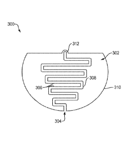
FIG. 3 schematically illustrates another embodiment
of a loop-gap resonator 300 according to the present
invention, wherein an interdigitated capacitor structure
302 defines a convoluted path, illustrated as a zig-zag
path, along a gap 304 having a plurality of legs 306 and
corresponding changes in direction 308, providing a
further increase in the length of the gap 304 and a
corresponding increase in capacitance, relative to the
loop-gap resonator 200 illustrated in FIG. 2. In the
illustrated embodiment, the zig-zag path of the gap 304
comprises eight reversals in direction. In various other
embodiments, the number of changes in direction designed
into the zig-zag path is determined by one or more of the
amount of capacitance desirable for a particular
application of a resonator, the amount of physical space
available in the resonator, and the width of the gap,
which is approximately inversely proportional to the
capacitance. Nonlimiting examples of embodiments include
any number from 2 through 38 changes in direction (as
illustrated in FIG. 4 hereinbelow) and any larger numbers
of changes in direction as may be required to achieve a
desired capacitance in a resonator.
In another embodiment, the lengths of consecutive
legs 306 along the path increases along the path from a
boundary 310 of the resonator 300 toward an opening 312
through the resonator 300. In yet another embodiment, a
diameter of the opening 312 is no larger than a width of
the gap 304. In a further embodiment, the opening 312
comprises a terminus of the gap 304. In still another
embodiment, the opening 312 comprises a semicircular end
of the gap 304. In addition, it can be seen in FIG. 3
- 12 -
CA 03075078 2020-03-05
W02019/051016
PCT/US2018/049649
that excess material has been removed from about the
opening along the boundary 310, which may provide a
further reduction of the inductance of the resonator.
FIG. 4 schematically illustrates still another
embodiment of a loop-gap resonator 400 according to the
present invention, wherein an interdigitated capacitor
structure 402 and corresponding zig-zag path along a gap
404 is configured to fill the majority of the area of the
resonator 400 between an opening 406 and a boundary 408
of the resonator 400, illustrating an exemplary
embodiment that maximizes the capacitance of the
resonator for a given gap width. In this embodiment, the
length of the legs first increases and then decreases
with distance from the opening 406, to maximize use of
the available surface area and capacitance of the
resonator 400. In an embodiment, the path follows
physical constraints associated with a design of the
resonator 400, such as attachment means 410 for mounting
the resonator 400 to another structure (not illustrated).
As illustrated, the resonator 400 is shown to comprise 38
reversals of direction in the zig-zag path. Modeling of
the embodiment of FIG. 4 using High Frequency
Electromagnetic Field System software from ANSYS Inc.,
Canonsburg, PA, predicted the radiation magnetic field in
the opening to be enhanced by a factor of approximately
21 relative to the prior-art loop-gap resonator design
illustrated in FIG. 1.
FIG. 5 schematically illustrates an exemplary
embodiment of a loop-gap resonator 500 according to the
present invention, including a tapered, interdigitated
capacitor structure 502. The resonator 500 is
approximately 1 cm in diameter and was fabricated from
oxygen-free copper using conventional machining methods.
- 13 -
CA 03075078 2020-03-05
W02019/051016
PCT/US2018/049649
In initial tests using a laboratory-made ESR
spectrometer, the resonator operated at its design
frequency of 1.5 GHz and had a Q (Quality) factor of 600.
A similar resonator having a straight path of a prior-art
design was found to have a frequency of 4.5 GHz and Q of
approximately 1500.
Loop-gap resonators according to the present
invention can provide high radiation fields in resonators
smaller in size than the wavelength of the radiation used
to interact with a sample contained therein, making them
excellent devices for controlling and measuring the
quantum state of qubits, which are fundamental building
blocks for quantum computing, using pulsed-radiation
techniques. FIG. 6 schematically illustrates a nanoscale
loop-gap resonator 600 according to the present
invention, for application to quantum computing. In one
embodiment the dimensions of the loop-gap resonator 600
are scaled to provide coupling to a single molecular
magnet, which would behave as a qubit. A resonator
according to the present invention would allow the
manipulation, control and read-out of the qubit's quantum
state. In an embodiment, the manipulation, control or
readout of the qubit's quantum state comprises the
application of pulses of electromagnetic radiation to the
resonator.
The resonator 600 is seen to comprise an opening 602
that functionally parallels the opening 406 of the
resonator 400 of FIG. 4. Also illustrated in FIG. 6 is a
portion of a gap 604 that functionally parallels the gap
404 illustrated in FIG. 4. The remainder of the gap 604
is not shown in FIG. 6, but follows a path functionally
similar to the interdigitated, zig-zag pattern of FIG. 4.
In a non-limiting example, the opening 602 contains a
- 14 -
CA 03075078 2020-03-05
WO 2019/051016
PCT/US2018/049649
sample 606 (illustrated as a circle in FIG. 6) comprising
a single magnetic molecule having a quantum state 608
(represented as an arrow) that can be manipulated,
controlled and measured using a spin-resonance technique
such as ESR or NMR (Nuclear Magnetic Resonance)
spectroscopy. In various embodiments the sample 606 can
be any chemical or molecular species suitable for
measurement using spin-resonance spectroscopic
techniques, or any quantum object that embodies a qubit,
nonlimiting examples of which include single magnetic
molecules, quantum dots, and nitrogen vacancy color
centers in diamond. Examples of suitable magnetic
species may include Cr7M molecular rings, where M can be a
transition-metal ion such as Ni, Co, or Mn. In an
embodiment, the quantum object is a superconducting
(Josephson) device. In a nonlimiting embodiment, the
opening 602 has a cross sectional dimension in the range
of one to 10 nanometers. In various embodiments, the
quantum state 608 is one of an electron spin state, or a
nuclear spin state. In an embodiment, the loop-gap
resonator 600 comprises a read-and-control circuit for
single or multiple qubits in a quantum computer.
An exemplary system according to the present
invention includes a loop-gap resonator of the present
invention, a sample positioned at least partially within
an opening of the resonator, a source of a magnetic field
that can be applied to the resonator, and a source of
electromagnetic radiation having a frequency selected to
match a resonance of the loop-gap resonator.
It is to be understood that although the invention
has been described above in terms of particular
embodiments, the foregoing embodiments are provided as
illustrative examples only, and do not limit or define
- 15 -
CA 03075078 2020-03-05
W02019/051016
PCT/US2018/049649
the scope of the invention. Various other embodiments,
including but not limited to the following, are also
within the scope of the claims. For example, elements
and components described herein may be further divided
into additional components or joined together to form
fewer components for performing the same functions.
Moreover, a resonator according to the present invention
can contain more than a single opening, with the path
connecting one opening to another instead of terminating
at a boundary.
In addition, resonators disclosed herein are
illustrated as being cylindrical, or circular and
substantially planar in shape, but many other shapes are
also possible, including other geometric shapes or more
complex shapes selected to optimize resonator
performance. Further, loop-gap resonators according to
the present invention can be fabricated as curved or
flexible devices. In addition to applications in ESR and
quantum computing, resonators of the present invention
have application in nuclear magnetic resonance (NMR) and
to other arts that employ high-frequency resonators.
What is claimed is:
- 16 -