Note: Descriptions are shown in the official language in which they were submitted.
CA 03075871 2020-03-13
WO 2019/059798
PCT/RU2017/000689
1
SEISMIC SENSOR
BACKGROUND
[cam The disclosure relates generally to devices for performing seismic
surveys.
More particularly, the disclosure relates to seismic sensors or nodes.
[0002] Seismic surveying, or reflection seismology, is used to map the Earth's
subsurface. A controlled seismic source emits low frequency seismic waves that
travel through the subsurface of the Earth. At interfaces between dissimilar
rock
layers, the seismic waves are partially reflected. The reflected waves return
to the
surface where they are detected by one or more seismic sensors. In particular,
the
seismic sensors detect and measure vibrations induced by the waves. Ground
vibrations detected by the seismic sensors at the earth surface can have a
very
wide dynamic range, with displacement distances ranging from centimeters to
angstroms. Data recorded by the seismic sensors is analyzed to reveal the
structure
and composition of the subsurface.
[0003] Conventional seismic sensors (e.g., geophones) are usually made with an
electric coil of wire immersed in a strong magnetic field. These
electromagnetic
sensors can be constructed as either moving magnet or moving coil types. In
the
moving coil version, the magnet is fixed to the case, which is then firmly
planted in
the earth. The moving electrical coil is immersed in the magnetic field gap of
the
fixed magnet and the coil is loosely coupled to the outer housing of the
sensor by
soft springs that restrict movement of the coil along a single axis. As the
coil moves
relative to the fixed magnet, it progressively cuts through lines of magnetic
flux,
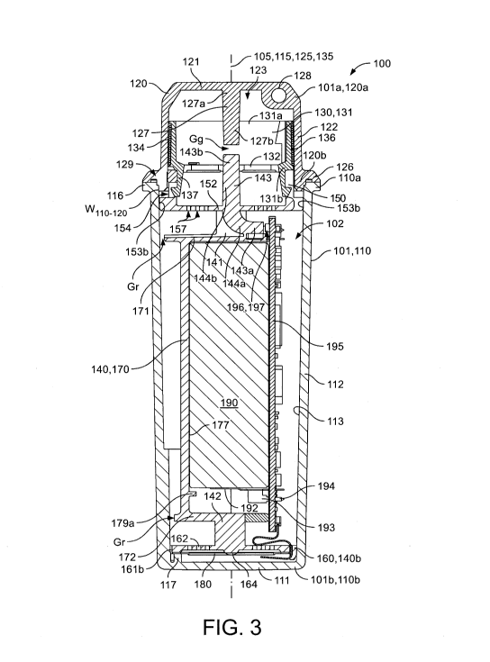
thereby generating a voltage and current at the electrical terminals of the
coil in
proportion to the velocity of ground displacement (e.g., vibrations). In the
moving
coil type, the coil defines the mass in the seismic sensor that moves in
response to
the ground vibrations.
[0004] Another type of seismic sensor relies on capacitance to generate the
electrical signal. These are typically constructed as Microelectromechanical
systems
(MEMS) using micro machined silicon with metal plating applied to facing
components on opposite sides of a small plated and spring loaded mass. These
MEMS sensors often have the advantage of small size and weight compared to a
CA 03075871 2020-03-13
WO 2019/059798
PCT/RU2017/000689
2
moving coil geophone. The movement of the MEMS proof mass relative to the
outer
fixed plates creates variable capacitance that is detected as a signal
proportional to
the acceleration of the sensor displacement.
BRIEF SUMMARY OF THE DISCLOSURE
[0005] Embodiments of seismic sensors for a seismic surveys are disclosed
herein.
In one embodiment, a seismic sensor comprises an outer housing having a
central
axis, a first end, and a second end opposite the first end. The first end
comprises a
portion made of a clear/transparent material configured to transmit light
having a
frequency in the visible or infrared range of the electromagnetic spectrum. In
addition, the seismic sensor comprises a proof mass moveably disposed in the
outer housing. The proof mass includes a power source. Further, the seismic
sensor comprises a sensor element disposed in the outer housing and configured
to
detect the movement of the outer housing relative to the proof mass. Still
further,
the seismic sensor comprises electronic circuitry coupled to the sensor
element and
the power source. Moreover, the seismic sensor comprises a light guide
assembly
having a first end adjacent the clear portion of the first end of the outer
housing and
a second end adjacent the electronic circuitry. The light guide assembly is
configured to transmit light in an axial direction between the first end of
the light
guide assembly and the clear section and to transmit light in a non-axial
direction
between the second end of the light guide assembly and the electronic
circuitry.
[0006] In another embodiment, a seismic sensor for a seismic survey comprises
an
outer housing having a central axis, a first end, and a second end opposite
the first
end. In addition, the seismic sensor comprises a proof mass moveably disposed
in
the outer housing. The proof mass includes a power source and electronic
circuitry
coupled to the power source. Further, the seismic sensor comprises a sensor
element disposed in the inner cavity and configured to detect the movement of
the
outer housing relative to the proof mass. The sensor element is coupled to the
electronic circuitry. Still further, the seismic sensor comprises a light
guide
assembly configured to transmit light from the electronic circuitry to the
outer
housing. The light guide assembly includes a first light guide fixably coupled
to the
proof mass and a second light guide fixably coupled to the outer housing.
CA 03075871 2020-03-13
WO 2019/059798
PCT/RU2017/000689
3
[0007] Embodiments described herein comprise a combination of features and
advantages intended to address various shortcomings associated with certain
prior
devices, systems, and methods. The foregoing has outlined rather broadly the
features and technical advantages of the invention in order that the detailed
description of the invention that follows may be better understood. The
various
characteristics described above, as well as other features, will be readily
apparent to
those skilled in the art upon reading the following detailed description, and
by
referring to the accompanying drawings. It should be appreciated by those
skilled in
the art that the conception and the specific embodiments disclosed may be
readily
utilized as a basis for modifying or designing other structures for carrying
out the
same purposes of the invention. It should also be realized by those skilled in
the art
that such equivalent constructions do not depart from the spirit and scope of
the
invention as set forth in the appended claims.
BRIEF DESCRIPTION OF THE DRAWINGS
[0008] For a detailed description of the preferred embodiments of the
invention,
reference will now be made to the accompanying drawings in which:
[0ow] Figure 1 is a schematic view of a seismic sensing system including a
plurality
of seismic sensors;
[0010] Figure 2 is a perspective view of an embodiment of a seismic sensor in
accordance with the principles described herein;
[0011] Figure 3 is a longitudinal cross-sectional view of the seismic sensor
of
Figure 2;
[0012] Figure 4 is a perspective end view of the end cap of Figure 2;
[0013] Figure 5 is an enlarged partial cross-sectional view of the seismic
sensor of
Figure 2 illustrating the coupling between the cap and the body of the outer
housing;
[0014] Figure 6 is a perspective view of the inductive spool assembly of
Figure 3;
[0015] Figure 7 is a perspective side view of the carrier of Figure 3;
[0016] Figure 8 is a perspective side view of the carrier of Figure 3;
[0017] Figure 9 is an enlarged cross-sectional view of the seismic sensor of
Figure
2;
CA 03075871 2020-03-13
WO 2019/059798
PCT/RU2017/000689
4
[0018] Figure 10 is an enlarged perspective view of the lower connection
member
and sensor element of Figure 3;
[0019] Figure 11 is a partial cross-sectional perspective view of the seismic
sensor
of Figure 2;
[0020] Figure 12 is a perspective view of the battery and the circuit board of
Figure
3;
[0021] Figure 13 is an enlarged perspective view of the battery, the circuit
board
and one tab of Figure 3;
[0022] Figure 14 is a perspective view of an embodiment of a seismic sensor in
accordance with the principles described herein;
[0023] Figure 15 is a longitudinal cross-sectional view of the seismic sensor
of
Figure 14;
[0024] Figure 16 is a top perspective partial cut away view of the seismic
sensor of
Figure 14;
[0025] Figure 17 is an enlarged perspective partial cut away view of the
seismic
sensor of Figure 14;
[0026] Figure 18 is an enlarged cross-sectional view of the seismic sensor of
Figure 14;
[0027] Figure 19 is an enlarged perspective partial cut-away view of the
seismic
sensor of Figure 14;
[0028] Figure 20 is an enlarged cross-sectional view of the seismic sensor of
Figure 14;
[0029] Figure 21 is a perspective view of the battery and tabs of Figure 16;
and
[0030] Figure 22 is a top view of an embodiment of a tab in accordance with
the
principles described herein.
DETAILED DESCRIPTION OF THE PREFERRED EMBODIMENTS
[0031] The following discussion is directed to various exemplary embodiments.
However, one skilled in the art will understand that the examples disclosed
herein
have broad application, and that the discussion of any embodiment is meant
only to
be exemplary of that embodiment, and not intended to suggest that the scope of
the
disclosure, including the claims, is limited to that embodiment.
CA 03075871 2020-03-13
WO 2019/059798
PCT/RU2017/000689
[0032] Certain terms are used throughout the following description and claims
to
refer to particular features or components. As one skilled in the art will
appreciate,
different persons may refer to the same feature or component by different
names.
This document does not intend to distinguish between components or features
that
5 differ in name but not function. The drawing figures are not necessarily
to scale.
Certain features and components herein may be shown exaggerated in scale or in
somewhat schematic form and some details of conventional elements may not be
shown in interest of clarity and conciseness.
[0033] In the following discussion and in the claims, the terms "including"
and
"comprising" are used in an open-ended fashion, and thus should be interpreted
to
mean "including, but not limited to... ." Also, the term "couple" or "couples"
is
intended to mean either an indirect or direct connection. Thus, if a first
device
couples to a second device, that connection may be through a direct
connection, or
through an indirect connection via other devices, components, and connections.
In
addition, as used herein, the terms "axial" and "axially" generally mean along
or
parallel to a central axis (e.g., central axis of a body or a port), while the
terms
"radial" and "radially" generally mean perpendicular to the central axis. For
instance, an axial distance refers to a distance measured along or parallel to
the
central axis, and a radial distance means a distance measured perpendicular to
the
central axis. Any reference to up or down in the description and the claims
will be
made for purposes of clarity, with "up", "upper", "upwardly" "down", "lower",
and
"downwardly" meaning the position or direction in normal use.
[0034] Referring now to Figure 1, a schematic representation of a seismic
surveying
system 50 for surveying a subsurface earthen formation 51 is shown. As shown
in
Figure 1, the subsurface 51 has a relatively uniform composition with the
exception
of layer 52, which may be, for example, a different type of rock as compared
to the
remainder of subsurface 51. As a result, layer 52 may have a different
density,
elastic velocity, etc. as compared to the remainder of subsurface 51.
[0035] Surveying system 50 includes a seismic source 54 disposed on the
surface
56 of the earth and a plurality of seismic sensors 64, 66, 68 firmly coupled
to the
surface 56. The seismic source 54 generates and outputs controlled seismic
waves
58, 60, 62 that are directed downward into the subsurface 51 and propagate
CA 03075871 2020-03-13
WO 2019/059798
PCT/RU2017/000689
6
through the subsurface 51. In general, seismic source 54 can be any suitable
seismic source known in the art including, without limitation, explosive
seismic
sources, vibroseis trucks and accelerated weight drop systems also known as
thumper trucks. For example, a thumper truck may strike the surface 56 of the
earth
with a weight or "hammer" creating a shock which propagates through the
subsurface 51 as seismic waves.
[0036] Due to the differences in the density and/or elastic velocity of layer
52 as
compared to the remainder of subsurface 51, the seismic waves 58, 60, 62 are
reflected, at least partially, from the surface of the layer 52. The reflected
seismic
waves 58', 60', 62' propagate upwards from layer 52 to the surface 56 where
they
are detected by seismic sensors 64, 66, 68.
[0037] The seismic source 54 may also induce surface interface waves 57 that
generally travel along the surface 56 with relatively slow velocities, and are
detected
concurrently with the deeper reflected seismic waves 58', 60', 62'. The
surface
interface waves 57 generally have a greater amplitude than the reflected
seismic
waves 58', 60', 62' due to cumulative effects of energy loss during
propagation of
the reflected seismic waves 58', 60', 62' such as geometrical spreading of the
wave
front, interface transmission loss, weak reflection coefficient and travel
path
absorption. The cumulative effect of these losses may amount to a 75dB, and in
cases more than 100dB, in amplitude difference between various waveforms
recorded by sensors 64, 66, 68.
[0038] The sensors 64, 66, 68 detect the various waves 57, 58', 60', 62', and
then
store and/or transmit data indicative of the detected waves 57, 58', 60', 62'.
This
data can be analyzed to determine information about the composition of the
subsurface 51 such as the location of layer 52.
[0039] Although seismic surveying system 50 is shown and described as a
surface
or land-based system, embodiments described herein can also be used in
connection with seismic surveys in transition zones (e.g., marsh or bog lands,
areas
of shallow water such as between land and sea) and marine seismic survey
systems in which the subsurface of the earthen formation (e.g., subsurface 51)
is
covered by a layer of water. In marine-based systems, the seismic sensors
(e.g.,
seismic sensors 64, 66, 68) may be positioned in or on the seabed, or
alternatively
CA 03075871 2020-03-13
WO 2019/059798
PCT/RU2017/000689
7
on or within the water. In addition, in such marine-based systems, alternative
types
of seismic sources (e.g., seismic sources 54) may be used including, without
limitation, air guns and plasma sound sources.
[0040] Referring now to Figures 2 and 3, an embodiment of a seismic sensor 100
is shown. In general, seismic sensor 100 can be used in any seismic survey
system. For example, sensor 100 can be used for any one or more of sensors 64,
66, 68 of seismic surveying system 50 shown in Figure 1 and described above.
Although sensor 100 can be used in land or marine seismic survey systems, it
is
particularly suited to land-based seismic surveys.
[0041] In this embodiment, seismic sensor 100 includes an outer housing 101,
an
inductive spool assembly 130 disposed within housing 101, a carrier 140
disposed
in housing 101 adjacent inductive spool assembly 130, and a sensor element 180
disposed within housing 101 and coupled to carrier 140. A power source or
supply
190 and electronic circuitry 195 are removably mounted to carrier 140 within
housing 101. In this embodiment, power supply 190 is a battery and electronic
circuitry 195 is in the form of a circuit board (e.g., PCB). Thus, power
supply 190
may also be referred to as battery 190 and electronic circuitry 195 may also
be
referred to as circuit board 195.
[0042] Referring still to Figures 2 and 3, housing 101 has a central or
longitudinal
.. axis 105, a first or upper end 101a, a second or lower end 101b, and an
inner
chamber or cavity 102. As will be described in more detail below, in this
embodiment, ends 101a, 101b are closed and inner cavity 102 is sealed and
isolated from the surrounding environment outside sensor 100, thereby
protecting
the sensitive components disposed within housing 101 from the environment
(e.g.,
water, dirt, etc.).
[0043] In this embodiment, housing 101 includes a generally cup-shaped body
110
and an inverted cup-shaped cap 120 fixably attached to body 110. In
particular,
body 110 has a central or longitudinal axis 115 coaxially aligned with axis
105, a
first or upper end 110a, and a second or lower end 110b defining lower end
101b
of housing 101. In addition, body 110 includes a planar cylindrical base 111
at
lower end 110b and a tubular sleeve 112 extending axially upward from base 111
to upper end 110a. Base 111 closes sleeve 112 at lower end 110b, however,
CA 03075871 2020-03-13
WO 2019/059798
PCT/RU2017/000689
8
sleeve 112 and body 110 are open at upper end 110a. As a result, body 110
includes a receptacle 113 extending axially from upper end 110a to base 111.
Receptacle 113 forms part of inner cavity 102 of housing 101. As will be
described in more detail below, open upper end 110a is closed with cap 120. An
annular flange 116 extends radially outward from sleeve 112 at upper end 110a
and an annular raised lip or shoulder 117 extends axially upward from base 111
into cavity 113. In this embodiment, the entire body 110 (including base 111,
sleeve 112, and flange 116) is made via injection molding into a single piece
of
polycarbonate.
[0044] Referring now to Figures 2-4, cap 120 has a central or longitudinal
axis 125
coaxially aligned with axis 105, a first or upper end 120a defining upper end
101a
of housing 101, and a second or lower end 120b. In this embodiment, cap 120
has the general shape of an inverted cup. In particular, cap 120 includes a
planar
cylindrical top 121 at upper end 120a and a tubular sleeve 122 extending
axially
downward from top 121 to lower end 120b. Top 121 closes sleeve 122 at upper
end 120a, however, sleeve 122 and cap 120 are open at lower end 120b. As a
result, cap 120 includes an inner chamber or cavity 123 extending axially from
lower end 120b to top 121. An annular flange 126 extends radially outward from
sleeve 122 proximal lower end 120b. In addition, an elongate cylindrical light
guide 127 extends axially downward from top 121 into cavity 113. Guide 127 is
coaxially disposed within cap 120 (e.g., guide 127 has a central axis
coaxially
aligned with axis 125) and has a first or upper end 127a fixably attached to
top 121
and a second or lower end 127b distal top 121.
[0045] As will be described in more detail below, guide 127 forms part of a
light
guide assembly for wirelessly communicating data to/from circuit board 195
through top 121 via the transmission of light. In embodiments described
herein,
the light transmitted by the light guide assembly has a frequency in the
visible or
infrared range of the electromagnetic spectrum (e.g., frequency of 3.0 THz to
300.0 THz and wavelength of 1.0 pm to 100 pm). In one embodiment, the light
transmitted by the light guide assembly is in the infrared range of the
electromagnetic spectrum with a wavelength of 850 nm. To facilitate the
transmission of light through guide 127, it is made of a clear/transparent
material,
CA 03075871 2020-03-13
WO 2019/059798
PCT/RU2017/000689
9
and to facilitate the transmission of light through top 121, it is made of a
clear/transparent material. In this embodiment, the entire cap 120 (including
top
121, sleeve 122, and guide 127) is made via injection molding into a single
piece
of clear polycarbonate.
.. [0046] As best shown in Figures 2 and 3, in this embodiment, a connector
128 is
provided on the outside of cap 120 at upper end 120a. In this embodiment,
connector 128 is an eye connector or throughbore to which a rope, lanyard,
hook,
carabiner or the like can be releasably attached. This can facilitate the
carrying of
sensor 100 during deployment and retrieval and/or facilitate the location of
sensors
100 for retrieval.
[0047] Referring now to Figure 3, cap 120 is fixably attached to body 110. In
particular, cap 120 is coaxially aligned with body 110 with lower end 120b of
cap
120 seated within upper end 110a of body 110 and annular flanges 116, 126
axially abutting each other. Body 110 and cap 120 are sized such that an
.. interference fit is provided between lower end 120b of cap 120 and upper
end
110a of body 110 when lower end 120b is seated in upper end 110a. In this
embodiment, body 110 and cap 120 are made of the same material
(polycarbonate), and thus, can be ultrasonically welded together to fixably
secure
cap 120 to body 110. More specifically, an annular ultrasonic weld W110-120 is
formed between the opposed radially outer surface and radially inner surface
of
sleeves 122, 112, respectively, at end 120b, 110a, respectively. Weld W110-120
defines an annular primary seal between cap 120 and body 110 that prevents
fluid
communication between cavities 113, 123 and the environment surrounding
sensor 100. In this embodiment, a secondary or backup annular seal assembly
.. 129 is provided between cap 120 and body 110. Seal assembly 129 includes an
annular 0-ring seal seated in an annular recess provided in the bottom surface
of
flange 126. The 0-ring seal is axially compressed between flanges 116, 126.
[0048] Referring now to Figures 3 and 6, inductive spool assembly 130 is used
to
inductively charge the battery 190 from the outside of sensor 100 (e.g.,
wirelessly).
In this embodiment, inductive spool assembly 130 includes a cylindrical sleeve-
shaped body 131 and a coil 136 wound around body 131. Coil 136 is electrically
coupled to circuit board 195 with wires (not shown) that enable the transfer
of
CA 03075871 2020-03-13
WO 2019/059798
PCT/RU2017/000689
current to circuit board 195, which in turn charges battery 190 during
charging
operations.
[0049] Body 131 has a central axis 135, a first or upper end 131a, and a
second or
lower end 131b. As best shown in Figure 3, assembly 130 is disposed within cap
5 120 with axes 135, 105 coaxially aligned. As shown in Figure 6, upper end
131a
is open, while a disc 132 extends across lower end 131b. Disc 132 is generally
oriented perpendicular to axis 135 and includes a central throughbore 133. The
radially outer surface of body 131 includes an annular recess 134 extending
axially
between ends 131a, 131b. Coil 136 is seated in recess 134 with the turns of
coil
10 136 axially adjacent one another. A pair of circumferentially-spaced
latches 137
and a pair of circumferentially-spaced guides 138 extend axially downward from
lower end 131b. Latches 137 releasably secure spool assembly 130 to carrier
140
such that assembly 130 cannot move rotationally or translationally relative to
carrier 140, and guides 138 slidingly engage an inner surface of carrier 140
to
facilitate the coaxial alignment of body 131 and carrier 140 during
installation of
assembly 130. In this embodiment, guides 138 are uniformly circumferentially-
spaced 180 apart, and latches 137 are uniformly circumferentially-spaced 180
apart, with one guide 138 disposed between each pair of circumferentially-
adjacent latches 137.
[0050] Referring now to Figures 3, 7, and 8, carrier 140 releasably supports
sensor
element 180, battery 190, and circuit board 195 within body 111 of outer
housing
110, and operates on sensor element 180 in response to vibrations induced by
seismic waves. In this embodiment, carrier 140 has a central or longitudinal
axis
145, a first or upper end 140a proximal upper end 111a of body 111, and a
second
or lower end 140b seated against shoulder 117 of body 110. As best shown in
Figure 3, carrier 140 is disposed within body 110 with axes 145, 105 coaxially
aligned.
[0051] Referring now to Figures 7 and 8, in this embodiment, carrier 140
includes
an upper connection member 150 at upper end 140a, a lower connection member
160 at lower end 140b, and a battery holder 170 axially positioned between
members 150, 160. An elongate upper post 141 couples upper connection
member 150 to battery holder 170 and an elongate lower post 142 couples lower
CA 03075871 2020-03-13
WO 2019/059798
PCT/RU2017/000689
11
connection member 160 to battery holder 170. Thus, post 141 is axially
positioned
between battery holder 170 and upper connection member 150, and post 142 is
axially positioned between battery holder 170 and lower connection member 160.
In this embodiment, connection members 150, 160, holder 170, and posts 141,
142 are concentrically disposed and coaxially aligned with housing 101. In
addition, in this embodiment, connection members 150, 160, holder 170, and
posts 141, 142 are monolithically formed as a unitary piece. In particular, in
this
embodiment, the entire carrier 140 is made as one monolithic piece by
injection
molding into a single piece of clear polycarbonate.
[0052] Upper connection member 150 has a first or upper end 150a defining
upper
end 140a of carrier 140 and a second or lower end 150b opposite end 150a. In
addition, upper connection member 150 includes an annular body 151 extending
axially between ends 150a, 150b, a flexure or biasing member 152 mounted to
body 151 at lower end 150b, and a generally annular mounting flange 153
extending radially outward from body 151 at lower end 150b. A pair of
uniformly
circumferentially-spaced through holes 154 extend radially through body 151.
Guides 138 of inductive spool assembly 130 are arranged (e.g., sized and
positioned) to slidingly engage the inner surface of sleeve 151 at upper end
150a,
while latches 137 releasably engage holes 154, thereby aligning and connecting
assembly 130 and connection member 150.
[0053] Referring again to Figures 7 and 8, mounting flange 153 extends
radially
outward from body 151. In this embodiment, flange 153 is not a continuous
annular flange, but rather, includes a plurality of circumferentially
extending
segments 153a. Each segment 153a has a radially outer cylindrical surface 153b
disposed at substantially the same radius as the inner surface of sleeve 112
of
body 110. In particular, cylindrical surfaces 153b of segments 153a are
fixably
secured to sleeve 112 proximal upper end 110a as shown in Figure 3. In
general,
segments 153a can be secured to sleeve 112 by any suitable means known in the
art including, without limitation, adhesive, interference fit, welded
connection, etc.
In this embodiment, upper connection member 150 and housing 110 are made of
polycarbonate, and thus, segments 153a are ultrasonically welded to sleeve 112
along surfaces 153b.
CA 03075871 2020-03-13
WO 2019/059798
PCT/RU2017/000689
12
[0054] Seismic sensor 100 may be provided with an electromagnetic shield.
Electromagnetic shields are known in the art and can shield the components of
the
sensor from radio frequency signals outside the sensor which might otherwise
interfere with operation of the components.
[0055] Referring now to Figures 3, 5, and 7, biasing member 152 is a
resilient,
flexible element that flexes and elastically deforms in response to relative
movement of outer housing 101 relative to battery holder 170 and the
components
mounted thereto (e.g., battery 190 and circuit board 195). In this embodiment,
biasing member 152 comprises an annular disc or flange 156 including a
plurality
of uniformly circumferentially-spaced through cuts or slots 157. Each slot 157
extends axially through disc 156. In addition, each slot 157 spirals radially
outward moving from a radially inner end proximal the center of disc 156 and a
radially outer end proximal body 151. In this embodiment, three slots 157 are
provided, each pair of circumferentially adjacent inner ends of slots 157 are
angularly spaced 120 apart about axis 145, each pair of circumferentially
adjacent
outer ends of slots 157 are angularly spaced 120 apart about axis 145, and
each
slot 157 extends along a spiral angle measured about axis 145 between its ends
of about 180 . As used herein, the term "spiral angle" refers to the angle
measured about an axis between the terminal ends of an object (e.g., angle
measured about axis 145 between the ends of a slot 157). The radially inner
ends
of slots 157 are radially spaced from the center of disc 156 and axis 145. As
a
result, a central portion of disc 156 provides a solid region on disc 156 to
which the
upper end of post 141 is fixably secured.
[0056] Biasing member 152 radially biases battery holder 170 and the
components
mounted thereto to a central or concentric position radially spaced from
housing
101 but does not substantially support or take up the weight of the battery
holder
170 and the components mounted thereto. Thus, biasing member 152 yields to
the weight of the battery holder 170 and components mounted thereto.. In
particular, disc 156 is a semi-rigid structure that generally resists flexing
and
bending. However, the presence of spiral slots 157 enhances the flexibility of
disc
156 in the region along which slots 157 are disposed (e.g., the region
radially
positioned between post 141 and segments 153a), thereby allowing that region
to
CA 03075871 2020-03-13
WO 2019/059798
PCT/RU2017/000689
13
flex in the axial direction (up and down) with relative ease. Spiral slots 157
also
enhance the flexibility of disc 156 in the radial direction. However, spiral
slots 157
do not allow disc 156 to flex as easily in the radial direction. Due to the
relatively
high degree of flexibility of biasing member 152 in the axial direction, when
an
axial load is applied to biasing member 152 by post 141, slots 157 generally
allow
the central portion of disc 156 to freely move axially up and down relative to
segments 153a. However, due to the more limited flexibility in the radial
direction,
when a radial load is applied to biasing member 152 by post 141, slots 157
generally resist the central portion of disc 156 from moving radially relative
to
segments 153a, and to the limited extent the central portion of disc 156 does
move
radially, disc 156 biases the central portion and post 141 back into coaxial
alignment with axes 105, 145.
[0057] As best shown in Figures 3 and 8, in this embodiment, an elongate
curved
L-shaped light guide 143 is coupled to upper connection member 150. Light
guide
143 has a first end 143a proximal circuit board 195, a second end 143b
proximal
lower end 127b of light guide 127, a first or horizontal portion 144a
extending
radially from end 143a, a second or vertical portion 144b extending axially
from
end 143b, and a 900 curve or bend extending between portions 144a, 144b.
Vertical portion 144b extends through the center of disc 156 of biasing member
152 and throughbore 133 of spool assembly 130, and is coaxially aligned with
light
guide 127 and housing 101. Similar to light guide 127, to facilitate
the
transmission of light, guide 143 is made of a clear/transparent material such
as
clear polycarbonate. As will be described in more detail below, light guides
127,
143 form the light guide assembly that wirelessly communicates data to/from
circuit board 195 through top 121. A gap Gg is axially positioned between ends
127b, 143b to allow relative axial movement between light guides 127, 143. Gap
Gg has a height measured axially between ends 127b, 143b that is preferably
minimized to reduce the loss of light transmitted between light guides 127,
143
across gap Gg, while allowing sufficient relative axial movement between light
guides 127, 143 as will be described in more detail below. In this embodiment,
relative axial movement of the light guides 127, 143 is about 10.0 microns,
and
thus, gap Gg is preferably at least 10 microns.
CA 03075871 2020-03-13
WO 2019/059798
PCT/RU2017/000689
14
[0058] Referring now to Figures 3 and 7-10, lower connection member 160
includes an annular mounting flange 161 and a flexure or biasing member 162
mounted to flange 156. In this embodiment, flange 161 is not a continuous
annular flange, but rather, includes a plurality of circumferentially
extending
segments 161a. Each segment 161a has a radially outer cylindrical surface 161b
disposed at substantially the same radius as the inner surface of sleeve 112
of
body 110. In particular, cylindrical surfaces 161b of segments 161a are
fixably
secured to sleeve 112 proximal lower end 110b as shown in Figure 9. In
general,
segments 161a can be secured to sleeve 112 by any suitable means known in the
art including, without limitation, adhesive, interference fit, welded
connection, etc.
In this embodiment, lower connection member 160 and housing 110 are made of
polycarbonate, and thus, segments 161a are ultrasonically welded to sleeve 112
along surfaces 161b. As best shown in Figures 8 and 10, flange 161 includes a
pair of circumferentially-spaced resilient fingers 163 that can be flexed
radially
outward to position sensor element 180 within flange 156 and then allowed to
spring radially inward to hold sensor element 180 in the desired position
within
flange 161.
[0059] Referring now to Figures 7-9, biasing member 162 is similar to biasing
member 152 previously described. In particular, biasing member 162 is a
resilient
element that flexes and elastically deforms in response to relative movement
of
outer housing 101 relative to battery holder 170 and the components mounted
thereto (e.g., battery 190 and circuit board 195). In addition, biasing member
162
comprises an annular disc or flange 156 as previously described. The lower end
of post 142 is fixably secured to the solid central region of disc 156 of
biasing
.. member 162. However, in this embodiment, biasing member 162 includes a semi-
spherical deflection inducer or button 164 and an annular support ridge or lip
166
extending axially from the bottom of disc 156. Button 164 is centered on disc
156,
and lip 166 is coaxially aligned with disc 156. In addition, lip 166 is
radially
positioned between slots 157 and mounting flange 161. Button 164 and lip 166
extend the same distance measured axially from the bottom of disc 156.
[0060] Referring now to Figures 9 and 10, sensor element 180 is a flat disc
seated
within mounting flange 161 against button 164 and lip 166 ¨ the tip of button
164
CA 03075871 2020-03-13
WO 2019/059798
PCT/RU2017/000689
engages the center of the upper surface of sensor element 180 and lip 166
engages the radially outer periphery of the upper surface of sensor element
180.
Fingers 163 hold sensor element 180 within flange 161 against button 164 and
lip
166. As best shown in Figure 9, shoulder 117 of body 110 is disposed at the
5 same radius as lip 166 and engages the radially outer periphery of the
lower
surface of sensor element 180 axially opposite lip 166. Thus, the outer
periphery
of sensor element 180 is compressed and fixed in position between shoulder 117
and lip 166.
[0061] In the same manner as biasing member 152 previously described, biasing
10 member 162 radially biases battery holder 170 and the components mounted
thereto to a central or concentric position radially spaced from housing 101,
but
does not substantially support or take up the weight of the battery holder 170
and
the components mounted thereto. Thus, biasing member 162 yields to the weight
of the battery holder 170 and components mounted thereto. Due to the
relatively
15 high degree of flexibility of biasing member 162 in the axial direction,
when an
axial load is applied to biasing member 162 by post 142, slots 157 generally
allow
the central portion of disc 156 to freely move axially up and down relative to
segments 153a. However, due to the more limited flexibility in the radial
direction,
when a radial load is applied to biasing member 162 by post 142, slots 157
generally resist the central portion of disc 156 from moving radially relative
to
segments 161a, and to the limited extent the central portion of disc 156 does
move
radially, disc 156 biases the central portion and post 142 back into coaxial
alignment with axes 105, 145.
[0062] Annular flanges 153, 161 are fixably secured to outer housing 101 and
posts 141, 142 coupled battery holder 170 to biasing members 152, 162,
respectively. Thus, weight of battery holder 170 and the components mounted
thereto cause biasing members 152, 162 to flex and yield in the axial
direction,
thereby bringing the tip of button 164 into contact with the center of sensor
element 180 and transferring substantially all of the weight of battery holder
170
and the components mounted thereto to the center of sensor element 180 (via
button 164).
CA 03075871 2020-03-13
WO 2019/059798
PCT/RU2017/000689
16
[0063] As best shown in Figure 9, the tip of button 164 contacts the center of
sensor element 180 and transfers the weight of battery holder 170 and the
components mounted thereto to sensor element 180 with outer housing 101 and
battery holder 170 at rest (e.g., no relative movement between outer housing
101
and battery holder 170). The outer periphery of sensor element 180 is
restrained
between lip 166 and shoulder 117, and thus, when button 164 bears against the
sensor element 180 under the weight of battery holder 170 and the components
mounted thereto, the outer periphery of sensor element 180 is static relative
to
housing 101.
[0064] Referring again to Figures 7 and 8, battery holder 170 has a first or
upper
end 170a and a second or lower end 170b. In addition, battery holder 170
includes a first or upper wall 171 disposed at upper end 170a, a second or
lower
wall 172 disposed at lower end 170b, and a semi-cylindrical body 173 extending
axially between walls 171, 172. Each wall 171, 172 is an annular plate or disc
including a rectangular recess 174 extending radially inward from the radially
outer
edge of the disc. Recesses 174 of walls 171, 172 are circumferentially aligned
and sized to receive circuit board 195 therein as shown in Figure 11. As best
shown in Figure 3, each wall 171, 172 has an outer radius that is less than
the
inner radius of outer housing 101. Thus, a gap Gr is radially positioned
between
each wall 171, 172 and housing 101. Each gap Gr has a width measured radially
between the wall 171, 172 and outer housing 101. In embodiments described
herein, the radial width of each gap Cr is preferably greater than 0.0 mm
(e.g.,
non-zero) and less than 2.0 mm, and more preferably greater than 0.0 mm and
less than 1.0 mm, with battery holder 170 concentrically disposed in outer
housing
101. The gap Gr allows outer housing 101 to move radially and laterally
relative to
battery holder 170 as discs 156 of biasing members 152, 162 flex, but limits
the
maximum such radial and lateral movement. Thus, walls 171, 172 function as
radial motion limiters or stops ¨ battery holder 180 can move radially within
housing 101 until wall 171, 172 radially contacts housing 101.
[0065] Referring again to Figures 7 and 8, a pair of uniformly
circumferentially-
spaced posts 176 extend axially from the radially outer periphery of each wall
171,
172. Posts 176 of upper wall 171 extends axially upward toward biasing member
CA 03075871 2020-03-13
WO 2019/059798
PCT/RU2017/000689
17
152 and posts 176 of wall 172 extend axially downward toward biasing member
162. However, the terminal ends of posts 176 are axially spaced from the
axially
adjacent biasing members 152, 162. Thus, a gap Ga is axially positioned
between
the terminal end of each post 176 and the axially adjacent biasing member 152,
162. Each gap Ga has a height measured axially between the terminal end of
each post 176 and the axially adjacent biasing member 152, 162. In embodiments
described herein, the axial height of each gap Ga is preferably about 10.0
microns,
with battery holder 170 in the neutral position in outer housing 101. As will
be
described in more detail below, gap Ga allows outer housing 101 to move
axially
relative to battery holder 170 as discs 156 of biasing members 152, 162 flex,
but
limits the maximum relative axial movement to a distance corresponding to the
size of gap Ga. Thus, posts 176 function as axial motion limiters or stops ¨
outer
housing 101 can move axially downward relative to battery holder 170 until
biasing
member 152 contact posts 176 extending from upper wall 171, and outer housing
101 can move axially upward relative to battery holder 170 until biasing
member
162 contacts posts 176 extending from lower wall 172. The minimum axial height
of gap Gg between ends 127b, 143b of guides 127, 143, respectively, is greater
than zero when posts 176 extending from wall 171 axially abut biasing member
152, thereby preventing ends 127b, 143b from contacting each other.
[0066] Referring now to Figures 7, 8, and 11, body 173 has lateral sides 173a,
173b extending axially between walls 171, 172 and a semi-cylindrical radially
inner
surface 177 extending circumferentially between sides 173a, 173b. Surface 177
defines a receptacle 178 sized and shaped to removably receive battery 190.
The
opening of receptacle 178 radially opposite surface 177 is circumferentially
aligned
with rectangular recesses 174 of walls 171, 172. A shoulder 179a is disposed
along and extends radially inward from surface 177. Shoulder 179a is axially
positioned proximal wall 172 and extends circumferentially between sides 173a,
173b. A plurality of axially spaced tabs 179b are provided along each side
173a,
173b. Tabs 179b extend circumferentially from sides 173a, 173b. As best shown
in Figure 11, battery 190 is seated in receptacle 178 against surface 177 and
axially positioned between wall 171 and shoulder 179a, which restrict and/or
prevent the axial movement of battery 190 relative to holder 170.
To
CA 03075871 2020-03-13
WO 2019/059798
PCT/RU2017/000689
18
accommodate thermal expansion of battery 190 and account for tolerances (e.g.,
the tolerance on the length of battery 190), the axial distance between wall
171
and shoulder 179a is preferably greater than the length of battery 190 and no
more than 2.0 mm greater than the length of battery 190, and more preferably
no
more than 1.0 mm greater than the length of batter 190, and still more
preferably
about 0.5 mm greater than the length of batter 190. Tabs 179b extend
circumferentially around battery 190, thereby retaining battery 190 within
receptacle 178. Tabs 179b are resilient members that can be flexed radially
outward to pass battery 190 therebetween during insertion or removal of
battery
190 from receptacle 178.
[0067] Referring now to Figures 7-11, as previously described, sensor element
180
is a flat disc disposed within flange 161 with button 164 and lip 166
contacting the
upper surface of element 180 and shoulder 117 and fingers 163 contacting the
lower surface of element 180. The radially outer periphery of element 180 is
generally held stationary relative to outer housing 101, however, the central
portion of element 180 bears the weight of battery holder 170 and the
components
mounted thereto, and further, can be deflected by button 164. In this
embodiment,
sensor element 180 is made of a metallic disc (e.g., brass) having one or more
layers of a piezoelectric ceramic material (e.g., lead zirconate titanate
(PZT))
disposed thereon. When mechanical stress is applied to sensor element 180 due
to deformation or deflection, the piezoelectric ceramic material generates an
electrical potential (piezoelectric effect). Sensor element 180 is
electrically coupled
to circuit board 195 with wires such that the electrical potential generated
by the
piezoelectric ceramic material is detected and measured by electronics housed
on
circuit board 195 and stored in memory on circuit board 195.
[0068] Referring now to Figure 12 and 13, battery 190 has a cylindrical shape
and
is coupled to circuit board 195 with a pair of tabs 191. In particular, tabs
191 are
disposed at the ends of battery 190 and are welded to battery 190. Tabs 191
are
made of metal (e.g., nickel plated stainless steel or nickel plated steel),
and
provide both a physical and electrical connection between battery 190 and
circuit
board 195. Thus, tabs 191 enable battery 190 to provide power to circuit board
195 and the various functions performed by the components of board 195 during
CA 03075871 2020-03-13
WO 2019/059798
PCT/RU2017/000689
19
seismic survey operations, and enable board 195 to provide power to battery
190
during inductive charging operations.
[0069] In this embodiment, each tab 191 is the same. More specifically, each
tab
191 is formed from relatively thin sheet metal. The sheet is stamped and then
bent such that each tab 191 includes a generally planar base 192, a pair of
supports 193 extending perpendicularly from the lateral sides of base 192, and
a
prong 194 extending from each support 193. Each base 192 is positioned flush
against the corresponding end of battery 190 and soldered thereto. Prongs 194
of
each tab 191 extend through circuit board 195 and are soldered thereto.
-- [0070] Referring now to Figures 3 and 11, battery 190 and circuit board 195
are
fixably coupled with tabs 191, and then that assembly is releasably coupled to
battery holder 170 by seating battery 190 in receptacle 178 as previously
described with board 195 circumferentially aligned with recesses 174. Thus,
when
battery 190 is disposed in receptacle 178, the ends of board 195 are disposed
in
-- recesses 174. Positioning circuit board 195 within recesses 174 spaces
board
195 away from housing 101, thereby reducing the potential for circuit board to
inadvertently contact or rub against housing 101. In addition, the lateral
sides of
recesses 174 prevent circuit board 195 and battery 190 coupled thereto from
rotating relative to carrier 140.
-- [0071] In this embodiment, battery 190 is coaxially aligned with carrier
140 and
housing 101. As will be described in more detail below, during seismic survey
operations, outer housing 101 and connection members 150, 160 axially
reciprocate relative to battery 190, circuit board 195, and battery holder 170
in
response to vibrations induced by seismic waves. Thus, in this embodiment,
-- battery 190, board 195, and battery holder 170 collectively define the
proof mass
of sensor 100. Tabs 191 are designed and configured to provide sufficient
rigidity
and strength to prevent battery 190 and circuit board 195 from moving axially
relative to each. In particular, bases 192 are generally oriented
perpendicular to
axes 105, 145. Since bases 192 are relatively thin in the axial direction,
they may
-- be prone to flexing in the axial direction. However, supports 193 are
oriented
perpendicular to the corresponding base 192 (e.g., parallel to axes 105, 145),
and
CA 03075871 2020-03-13
WO 2019/059798
PCT/RU2017/000689
thus, enhance the rigidity and strength to bases 192 in the axial direction,
thereby
limiting and/or preventing bases 192 from flexing.
[0072] Circuit board 195 includes the electronic circuitry of sensor 100. The
electronic circuitry is coupled to sensor element 180 and is arranged to
process the
5 output of sensor element 180, for example by amplifying, digitally
sampling,
transmitting and/or storing the output of sensor element 180. In addition, an
LED
196 and a photodiode 197 are mounted to circuit boards 195 and coupled to the
electronic circuitry. LED 196 and photodiode 197 are positioned adjacent each
other on the face of circuit board 195 immediately adjacent end 143a of light
guide
10 143. Together, top 121, light guides 127, 143, LED 196, and photodiode
197
enable the bidirectional communication of data to/from circuit board 195. In
particular, a device outside sensor 100 can wirelessly communicate with
circuit
board 195 via the transmission of light from the external device through top
121 and
guide 127 to end 127b, across gap Gg from end 127b to end 143b, through guide
15 143 to end 143a, and across the gap between end 143a and photodiode 197
to
photodiode 197; and circuit board 195 can wirelessly communicate with the
external
device via the transmission of light from LED 196 across the gap between LED
196
and end 143a into guide 143, through guide 143 to end 143b, across gap Gg from
end 143b to end 127b, and through guide 127 and top 121 to the external
device.
20 [0073] During seismic surveys, a plurality of sensors 100 are placed on
or in the
surface of the earth (e.g., in place of sensors 64, 66, 68 in system 50). Each
sensor 100 may, for example, be attached to a spike which is pushed into the
earth. Alternatively, the entire sensor 100 may be buried, or placed at depth
in a
borehole. Regardless of how sensors 100 are coupled to the earth, each sensor
100 is preferably positioned with axis 105 oriented in a generally vertical
direction.
Biasing members 152, 162 flex under the weight of the proof mass (e.g., the
weight of the assembly of battery 190, board 195, and battery holder 170),
thereby
transferring the weight of the proof mass to sensor element 180 via button
164.
[0074] The arrival of a compressional seismic wave causes outer housing 101
and
the components fixably coupled thereto (e.g., spool assembly 130, body 151 and
mounting flange 153 of upper connection member 150, and mounting flange 161
of lower connection member 160) to move and reciprocate in a generally
vertical
CA 03075871 2020-03-13
WO 2019/059798
PCT/RU2017/000689
21
direction. The inertia of the proof mass within outer housing 101 (e.g., the
assembly of battery 190, board 195, and battery holder 170) causes the proof
mass to resist moving with the displacement of the outer housing 101, and
consequently there is axial movement of the outer housing 101 relative to the
proof mass, as permitted by biasing members 152, 162, walls 171, 172, and
posts
176. This movement causes biasing members 152, 162 to flex or be deflected.
Button 164 bears against sensor element 180 with sensor 100 at rest and during
receipt of seismic waves. Thus, the deflection of biasing members 152, 162
varies
the load applied to sensing element 180 by button 164. The axial reciprocation
of
the outer housing 101 relative to the proof mass generally continues as the
compressional seismic wave passes across sensor 100.
[0075] During the axial reciprocations of the outer housing 101 relative to
the proof
mass, the sensor element 180 is cyclically deflected by button 164. As
previously
described, when mechanical stress is applied to sensor element 180 due to
deformation or deflection by button 164, the piezoelectric ceramic material
generates an electrical potential (piezoelectric effect). The electrical
potential is
connected to circuit board 195 via wires, where it is detected, and may be
sampled
and stored in memory as a measure of the amplitude of the seismic vibration.
The
data stored in memory on the circuit board 195 can be communicated to an
external
device for further consideration and analysis via LED 196, light guides 127,
143, and
top 121 as previously described.
[0076] As previously described, circuit board 195 forms part of the proof mass
that
outer housing 101 moves axially relative to during seismic surveying. Thus,
outer
housing 101 moves axially relative to LED 196 and photodiode 197 of circuit
board
195. The two-part light guide assembly including light guides 127, 143 allows
for
bi-directional communications to/from circuit board 195 despite the relative
axial
movement of the outer housing 101 relative to the proof mass, associated LED
196, and photodiode 197. In particular, gap Gg allows light guides 127, 143 to
move axially relative to each other as light guide 127 moves axially with
outer
housing 101 and light guide 143 moves axially with post 141. Thus, end 143a
remains aligned with LED 196 and photodiode 197 during relative axial movement
of outer housing 101 relative to the proof mass. The coaxial alignment of
guide
CA 03075871 2020-03-13
WO 2019/059798
PCT/RU2017/000689
22
127, portion 144b of guide 143, and outer housing 101 (including cap 120)
ensures alignment of ends 127b, 141b and enables the transmission of light
through guides 127, 143 despite the relative axial movement. In addition, the
coaxial alignment of guide 127 and portion 144b of guide 143 with the center
of
cap 120 enables the transmission of light through guides 127, 143 and cap 120
regardless of the rotational orientation of cap 120 relative to carrier 140.
It should
also be appreciated that the L-shape of light guide 143 enables the transfer
of light
to/from photodiode 197 and LED 196, respectively, which generally face in a
radial
direction (generally face toward axis 105) while ensuring the coaxial and
centered
alignment of cap 120, guide 127, and portion 144b. In embodiments described
herein, the light guide assemblies rely on the transmission of light via total
internal
reflection (TIR) as is known in the art. Without being limited by this or any
particular theory, for light guide assemblies described herein that are made
of
clear polycarbonate, light incident on an internal wall of the light guide
assembly at
an angle less than about 430 is internally reflected. However, it should be
appreciated that the incident angle resulting in internal reflection may
depend on a
variety of factors including the material of the light guide assembly.
[0077] As previously described, biasing members 152, 162 allow generally free
relative axial movement of the proof mass relative to the outer housing 101.
In the
resting position, button 164 engages sensor element 180, and further, sensor
element 180 supports the majority or substantially all of the weight of the
battery
190. Consequently, sensor element 180 is subjected to stress with the proof
mass
in the resting position. The axial reciprocation of the outer housing 101
relative to
the proof mass subjects sensor element 180 to increasing and decreasing
degrees
of stress. The variations in the stress experienced by the sensor element 180
is
used to detect and measure the seismic waves. However, it should be
appreciated that the ceramic material of the sensor element 180 may be damaged
by excessive stress. Accordingly, the maximum axial movement of outer housing
101 relative to the proof mass is limited to protect the sensor element 180
and
prevent it from being overly stress. In the embodiment of sensor 100 shown and
described above, the maximum axial movement of the outer housing 101 relative
to the proof mass is controlled and limited by posts 176 as previously
described.
CA 03075871 2020-03-13
WO 2019/059798
PCT/RU2017/000689
23
In addition, as previously described, biasing members 152, 162 bias the proof
mass to the centered position coaxially aligned with outer housing 101. As a
result, the proof mass is radially spaced from outer housing 101 and is
generally
restrained from moving radially relative to the outer housing 101.
Consequently,
the movement of outer housing 101 relative to the proof mass is predominately
in
the axial direction, and further, the proof mass does not inhibit or interfere
with the
axial movement of outer housing 101. It should be appreciated that the gaps Gr
also limit the relative radial movement between outer housing 101 and the
proof
mass to ensure predominantly axial motion.
[0078] Although slots 157 having spiral geometries are employed to enhance the
flexibility of disc 156 and biasing member 152, 162 in the axial direction in
this
embodiment of sensor 100, in other embodiments, different approaches can be
used to enhance the flexibility of the disc. For example, slots having
different
geometries can be employed (e.g., radially extending slots as opposed to
spiral
slots). As another example, the disc of each biasing member (e.g., disc 156 of
each biasing member 152, 162) includes radially extending spokes or bridges
extending between an outer periphery of the disc and the central portion of
the
disc, thereby creating a plurality of circumferentially-spaced pie shaped
slots in the
disc between each pair of adjacent spokes. As yet another example, different
materials can be used to form the disc, or the thickness or geometry of the
disc
can be varied (e.g., thinner disc), etc. As used herein, term "slot" may
generally
be used to refer to a cut or hole, and thus, should not be interpreted to
refer to a
specific geometry of cut or hole unless expressly stated.
[0079] A second embodiment of a seismic sensor 200 will now be described in
connection with Figures 14-21. In the second embodiment, the electrical
connections between the battery and the electronic circuitry are resilient and
function similarly to biasing members 152, 162 previously described. In
general,
seismic sensor 200 can be used in any seismic survey system. For example,
sensor 200 can be used for any one or more of sensors 64, 66, 68 of seismic
surveying system 50 shown in Figure 1 and described above. Although sensor
200 can be used in a land seismic survey system, a transition zone seismic
survey
CA 03075871 2020-03-13
WO 2019/059798
PCT/RU2017/000689
24
system, or marine seismic survey system, it is particularly suited to land-
based
seismic surveys and transition zone seismic survey systems.
[0080] Referring now to Figures 14-16, in this embodiment, seismic sensor 200
includes an outer housing 201, an inductive spool assembly 230 disposed within
housing 201, a carrier 240 disposed in housing 201, and a sensor element 180
disposed within housing 201 and coupled to carrier 240. Electronic circuitry
195 is
fixably mounted to carrier 240 within housing 201, however, battery 190 is
configured to move axially relative to housing 201, carrier 240, and circuitry
195.
Sensor element 180, battery 190, and circuitry 195 of sensor 200 are the same
as
previously described with respect to sensor 100. Thus, electronic circuitry
195 is
in the form of a circuit board (e.g., PCB).
[0081] Housing 201 is substantially the same as housing 101 previously
described.
In particular, housing 201 has a central or longitudinal axis 205, a first or
upper
end 201a, a second or lower end 201b, and an inner chamber or cavity 202. Ends
201a, 201b are closed and inner cavity 202 is sealed and isolated from the
surrounding environment outside sensor 200, thereby protecting the sensitive
components disposed within housing 201 from the environment (e.g., water,
dirt,
etc.). In addition, housing 201 includes a generally cup-shaped body 210 and
an
inverted cup-shaped cap 220 fixably attached to body 210.
[0082] Body 210 has a central or longitudinal axis 215 coaxially aligned with
axis
205, a first or upper end 210a, and a second or lower end 210b defining lower
end
201b of housing 201. In addition, body 210 includes a base 211 at lower end
210b
and a tubular sleeve 212 extending axially upward from base 211 to upper end
110a. Base 211 closes sleeve 212 at lower end 210b, however, sleeve 212 and
body 210 are open at upper end 210a. As a result, body 210 includes a
receptacle 213 extending axially from upper end 210a to base 211. Receptacle
213 forms part of inner cavity 202 of housing 201. As best shown in Figures 15
and 19, at the lower end of receptacle 213 axially adjacent base 211, body 210
includes an annular upward-facing planar shoulder 214 radially adjacent sleeve
212 and an upward-facing circular planar surface 216 concentrically positioned
within shoulder 214. A recess 217 is provided along a portion of shoulder 214.
As
CA 03075871 2020-03-13
WO 2019/059798
PCT/RU2017/000689
will be described in more detail below, open upper end 210a is closed with cap
220.
[0083] In this embodiment, body 210 of outer housing 201 includes a pair of
connectors 218a, 218b. Connector 218a is provided on base 211 and connector
5 218b is provided along sleeve 212. Connector 218a includes rectangular
throughbore 219a extending radially therethrough and a hole 219b extending
axially from lower end 210b to throughbore 219a. Hole 219b is internally
threaded
and threadably receives the externally threaded end of a spike used to secure
sensor 200 to the ground. Throughbore 219a enables a rope or the like to be
10 attached to sensor 200 for storage or deployment. In particular, the
rope may be
folded double and inserted through bore 219a. Thus, bore 219a has a width of
at
least twice the diameter of the rope. The loop formed by the portion of folded
rope
extending through bore 219a is then placed around the sensor 200. In this
manner, a plurality of sensors 200 can be coupled to a single rope without
side
15 ropes, hooks or other mechanisms that can complicate the handling of
multiple
sensors.
[0084] A connector 218b is disposed along the outside of sleeve 212 proximal
upper end 201a. In general, connector 218b provides an alternative means for
handling of sensor 200 during deployment and retrieval. In this embodiment,
20 connector 218b is an eye connector or throughbore to which a rope,
lanyard, hook,
carabiner or the like can be releasably attached. Connector 218b can also be
used in a manner similar to throughbore 219a, thereby allowing a rope to be
folded
double and inserted through the hole of connector 218b. Thus, the bore of
connector 218a has a width of at least twice the diameter of the rope. The
loop
25 formed by the portion of folded rope extending through the bore of
connector 218b
is then placed around the sensor 200. In this manner, a plurality of sensors
200
can be coupled to a single rope without side ropes, hooks or other mechanisms
that can complicate the handling of multiple sensors. In this embodiment, the
entire body 110 (including base 211 and sleeve 212) is made via injection
molding.
[0085] Referring still to Figures 14-16, cap 220 has a central or longitudinal
axis
225 coaxially aligned with axis 205, a first or upper end 220a defining upper
end
201a of housing 201, and a second or lower end 220b. In this embodiment, cap
CA 03075871 2020-03-13
WO 2019/059798
PCT/RU2017/000689
26
220 has the general shape of an inverted cup. In particular, cap 220 includes
a
planar cylindrical top 221 at upper end 220a and a tubular sleeve 222
extending
axially downward from top 221 to lower end 220b. Top 221 closes sleeve 222 at
upper end 220a, however, sleeve 222 and cap 220 are open at lower end 220b.
As a result, cap 220 includes an inner chamber or cavity 223 extending axially
from lower end 220b to top 221. An annular flange 226 extends radially outward
from sleeve 222 proximal lower end 220b. An annular recess 227 is provided
along the bottom surface of flange 226.
[0086] As best shown in Figures 15 and 16, cap 220 is fixably attached to body
210. In particular, cap 220 is coaxially aligned with body 210 with lower end
220b
of cap 220 seated within upper end 210a of body 210 and upper end 210a of body
210 seated in annular recess 227 of flange 226. Body 210 and cap 220 are sized
such that an interference fit is provided between lower end 220b of cap 220
and
upper end 210a of body 210, and an interference fit is provided between upper
end 210a of body 210 and recess 227. In this embodiment, body 210 and cap 220
are made of the same material (polycarbonate), and thus, are can be
ultrasonically
welded together to fixably secure cap 220 to body 210. More specifically, an
annular ultrasonic weld W210-220 is formed between the opposed radially outer
surface and radially inner surface of sleeves 222, 212, respectively, at ends
220b,
210a. Weld W210-220 defines an annular seal between cap 220 and body 210 that
prevents fluid communication between cavities 213, 223 and the environment
surrounding sensor 200.
[0087] Referring still to Figures 15 and 16, inductive spool assembly 230 is
used to
inductively charge the battery 190 from the outside of sensor 100 (e.g.,
wirelessly).
In this embodiment, spool assembly 230 is substantially the same as inductive
spool assembly 130 previously described with the exception that spool assembly
230 does not include latches 137 or guides 138. Thus, spool assembly 230
includes annular body 131 and coil 136 wound around body 131. Body 131 is
disposed about the upper portion of carrier 240. Coil 136 is electrically
coupled to
circuit board 195 with wires (not shown) that enable the transfer of current
to
circuit board 195, which in turn charges battery 190 during charging
operations.
CA 03075871 2020-03-13
WO 2019/059798
PCT/RU2017/000689
27
[0088] In this embodiment, carrier 240 supports circuit board 195 and a light
guide
228 within body 211 of outer housing 210, and further, carrier 240 operates on
sensor element 180 in response to vibrations induced by seismic waves.
However, unlike sensor 100 previously described, in this embodiment, battery
190
.. is moveably disposed within carrier 240. In particular, carrier 240,
circuit board
195, and light guide 228 are fixably coupled to outer housing 201 and do not
move
relative to outer housing 210, however, battery 190 is movably coupled to
carrier
240, and thus, battery 190 can move axially relative to carrier 240, circuit
board
195, light guide 228, and outer housing 201.
[0089] As best shown in Figures 15 and 16, carrier 240 has a central or
longitudinal axis 245 coaxially aligned with axis 205, a first or upper end
240a
extending through inductive spool assembly 230, a second or lower end 240b
axially adjacent base 211, and a radially outer surface 241 extending axially
from
upper end 240a to lower end 240b. Outer surface 241 slidingly engages the
inside
.. of outer housing 201 between ends 240a, 240b. In particular, outer surface
241
includes a first cylindrical surface 241a proximal upper end 240a, a second
cylindrical surface 241b axially adjacent surface 241a, and a third
cylindrical
surface 241c axially adjacent surface 241b and extending axially from lower
end
240b. Thus, cylindrical surface 241b is axially positioned between surfaces
241a,
241c. Surfaces 241a, 241b, 241c are disposed at different radii ¨ surface 241a
is
disposed at a radius that is less than surface 241b, and surface 241b is
disposed
at a radius that is less than surface 241c. Thus, upward facing planar annular
shoulders extend radially between each pair of axially adjacent surfaces 241a,
241b, 241c. Surface 241a extends through and slidingly engages the cylindrical
inner surface of body 131, surface 241b is disposed within and slidingly
engages
the cylindrical inner surface of cap 220, and surface 241c is disposed within
and
slidingly engages the cylindrical inner surface of sleeve 212. Radial
engagement
of these surfaces prevents carrier 240 from moving radially or laterally
relative to
outer housing 201. In this embodiment, the cylindrical inner surface of sleeve
212
includes a pair of axially extending splines that slidingly engage a
corresponding
pair of mating axially extending recesses provided on outer surface 241c.
CA 03075871 2020-03-13
WO 2019/059798
PCT/RU2017/000689
28
Engagement of these mating splines and recesses prevents carrier 240 from
rotating about axis 205 relative to outer housing 201.
[0090] Although surfaces 241a, 241b, 241c of outer surface 241 are described
as
being cylindrical, it should be appreciated that outer surface 241 of carrier
240
may include cavities or recesses (e.g., to reduce its weight, to facilitate
its
manufacture by injection molding, etc.). In addition, outer surface 241
includes a
planar surface 242 extending axially from upper end 240a to lower end 240b.
Planar surface 242 is oriented parallel to axis 245, is radially offset from
axis 245,
and provides a face against which circuit board 195 can be mounted. Despite
the
foregoing, outer surface 241 slidingly engages each of cap 211, sleeve 212,
and
body 131 over an angular distance of at least 180 measured about axes 205,
245, which prevents carrier 240 from moving radially and laterally relative to
outer
housing 201.
[0091] Carrier 240 has an axial length that is substantially the same as the
axial
length of cavity 223. Thus, upper end 240a engages top 221 of cap 220 and
lower
end 240b is seated against sensing disk 180, which in turn is supported by
shoulder 214. More specifically, carrier 240 is axially compressed between cap
220 and outer housing 210. As a result, carrier 240 cannot move axially
relative to
outer housing 201.
[0092] Referring still to Figures 15 and 16, carrier 240 includes a recess or
pocket
244 that extends radially inward from outer surface 241, and in particular,
planar
surface 242. Pocket 244 is defined by an upper end surface 246, a lower end
surface 247, and a cylindrical surface 248 extending axially between end
surfaces
246, 247. Battery 190 is disposed within pocket 244 but does not contact
carrier
240. In particular, the dimensions of pocket 244 are greater than the
dimensions
of battery 190 (e.g., the radius of surface 248 is greater than the outer
radius of
battery 190, and the axial distance between end surfaces 246, 247 is greater
than
the length of battery 190). In this embodiment, battery 190 is oriented
parallel to
axes 205, 245, but is slightly radially offset from axes 205, 245. In
particular, the
central axis of battery 190 is radially offset from axes 205, 245 by about 1.0
to 1.5
MM.
CA 03075871 2020-03-13
WO 2019/059798
PCT/RU2017/000689
29
[0093] Referring now to Figures 15-20, an annular recess 250 extends radially
outward from pocket 244 and into surface 248 proximal upper end surface 246
and an annular recess 251 extends radially outward from pocket 244 and into
surface 248 proximal lower end surface 247. As best shown in Figures 18 and
20,
a rectangular hole 252 extends radially from recess 250 and surface 248 to
outer
surface 241c proximal upper end surface 246, and a rectangular hole 253
extends
radially from recess 251 and surface 248 to outer surface 241c proximal lower
end
surface 247. As best shown in Figures 17 and 18, end surface 246 is axially
spaced above recess 250 and hole 252, and as best shown in Figures 19 and 20,
end surface 247 is axially spaced below recess 251 and hole 253.
[0094] Referring now to Figures 16 and 18, elongate curved L-shaped light
guide
228 is fixably secured to carrier 240. In this embodiment, light guide 228 is
integral with and monolithically formed with carrier 240. Light guide 228 has
a first
end 228a proximal circuit board 195, a second end 228b engaging or immediately
adjacent top 221, a first or horizontal portion 229a extending radially from
end
228a, a second or vertical portion 229b extending axially from end 143b, and a
substantially 90 curve or bend extending between portions 229a, 229b.
Horizontal portion 229a extends through surface 241a and vertical portion 229b
extends to upper end 240a. In addition, vertical portion 229b is coaxially
aligned
with carrier 240 and housing 201. As will be described in more detail below,
light
guide 228 wirelessly communicates data to/from circuit board 195 through top
221.
To facilitate the transmission of light, light guide 228 and top 221 are made
of a
clear material. In this embodiment, the entire cap 220 (including top 221 and
sleeve 222) and guide 228 are made of a clear polycarbonate.
[0095] Referring now to Figures 19 and 20, a generally circular recess 260 is
provided in lower end 240b of carrier 240. Recess 260 is coaxially aligned
with
battery 190 and pocket 244, and has a radius slightly less than the radius of
carrier
240 at lower end 240b. As a result, lower end 240b of carrier 240 is an
annular
downward facing planar surface. Recess 260 extends axially from lower end 240b
to an annular flange 261 axially positioned between recess 260 and pocket 244.
The planar upper surface of flange 261 defines lower end surface 247 of pocket
244, and the planar lower surface of flange 261 defines the upper end of
recess
CA 03075871 2020-03-13
WO 2019/059798
PCT/RU2017/000689
260. A central throughbore 262 extends axially through flange 261 and a
cylindrical post 263 is coaxially disposed in throughbore 262. Recess 260,
throughbore 262, and post 263 are coaxially aligned with battery 190. A thin
arm
or blade 264 extends between post 263 and flange 261, thereby maintaining post
5 .. 263 in position within throughbore 262. As will be described in more
detail below,
post 263 can freely move axially within throughbore 262 as outer housing 201
and
carrier 240 axially reciprocate. The thin arm extending between post 263 and
flange 261 does not inhibit the axial movement of outer housing 201 and
carrier
240 relative to post 263. Although post 263 is coupled to flange 261 with a
thin
10 arm or blade in this embodiment, in other embodiments, the post (e.g.,
post 263) is
not coupled to the flange and instead, is attached to a battery tab (e.g., tab
290
described in more detail below) or sensor element 180.
[0096] Referring now to Figures 16, 19, and 20, sensor element 180 is a flat
disc
axially positioned between lower end 240b and shoulder 214. End 240b and
15 shoulder 214 are disposed at the same radius and engage the radially outer
periphery of the upper and lower surfaces of element 180, respectively. In
addition, post 263 engages the center of the upper surface of sensor element
180.
Thus, the outer periphery of sensor element 180 is compressed and fixed in
position between end 240b and shoulder 214. Thus, the radially outer periphery
of
20 .. element 180 is generally held static relative to housing 201 and carrier
240,
however, the central portion of element 180 can be deflected with post 263.
Planar surface 216 is axially spaced below sensor element 180 (e.g., there is
a
gap between planar surface 216 and sensor element 180), thereby allowing post
263 to deflect or flex the central portion of element 180. As previously
described,
25 sensor element 180 is made of a metallic disc (e.g., brass) having one
or more
layers of a piezoelectric ceramic material (e.g., lead zirconate titanate
(PZT))
disposed thereon. When mechanical stress is applied to sensor element 180 due
to deformation or deflection, the piezoelectric ceramic material generates an
electrical potential (piezoelectric effect). Sensor element 180 is
electrically coupled
30 .. to circuit board 195 with wires such that the electrical potential
generated by the
piezoelectric ceramic material is detected and measured by electronics housed
on
circuit board 195 and stored in memory on circuit board 195. Since axial
CA 03075871 2020-03-13
WO 2019/059798
PCT/RU2017/000689
31
movement of sensor element 180 relative to post 263 while post 263 engages
sensor element 180 induces stress in sensor element 180, post 263 may also be
referred to herein as a pusher or actuator.
[0097] Referring now to Figure 16, 18, and 21, battery 190 has a cylindrical
shape
and is coupled to circuit board 195 with a pair of tabs 290. In particular,
tabs 290
are disposed at the ends of battery 190 and are spring loaded to axially
compress
battery 190 therebetween. Tabs 290 are made of metal (e.g., steel), and
provide
both a physical and electrical connection between battery 190 and circuit
board
195. Thus, tabs 290 enable battery 190 to provide power to circuit board 195
and
the various functions performed by the components of board 195 during seismic
survey operations, and enable board 195 to provide power to battery 190 during
inductive charging operations.
[0098] In this embodiment, each tab 290 is a resilient, semi-rigid element
through
which battery 190 is supported within pocket 244 of carrier 240. As best shown
in
.. Figure 21, each tab 290 comprises a disc 291, a plurality of prongs 292
extending
laterally from disc 291, and a connector 293 extending radially from disc 291.
As
best shown in Figure 21, disc 291 has a semi-cylindrical shape including a
straight
edge 291a and a semi-circular edge 291b extending from side 291a. Prongs 292
extend from edge 291a and connector 293 extends from semi-circular edge 291b
opposite prongs 292.
[0099] For purposes of clarity and further explanation, the tab 290 coupled to
the
top of battery 190 may be referred to as the upper tab 290 and the tab 290
coupled to the bottom of battery 190 may be referred to as the lower tab 290.
As
shown in Figures 15-20, the semi-circular edge 291b of upper tab 290 is seated
in
recess 250 of carrier 240 and the semi-circular edge 291b of lower tab 290 is
seated in recess 251 of carrier 240. As best shown in Figures 18 and 20,
connector 293 of upper tab 290 is seated in mating hole 252 and connector 293
of
lower tab 290 is seated in mating hole 253. The positioning of edges 291b in
recesses 250, 251 maintains the outer periphery of tabs 290 static or fixed
relative
to carrier 240 and outer housing 201, and the positioning of connectors 293 in
holes 252, 253 prevents tabs 290 from rotating relative to carrier 240 and
outer
CA 03075871 2020-03-13
WO 2019/059798
PCT/RU2017/000689
32
housing 201. Prongs 292 of each tab 290 extend through circuit board 195 and
are soldered thereto.
[00100]Referring now to Figures 18 and 20, each tab 290 includes a central
projection 296 extending axially therefrom and a plurality of uniformly
circumferentially-spaced through cuts or slots 297 radially positioned between
projection 296 and edges 291a, 291b. Tabs 290 are oriented such that central
projections 296 face and extend toward battery 190. In addition, projection
296 of
upper tab 290 is fixably coupled to the upper end of battery 190 and the
central
projection 296 of lower tab 290 is fixably coupled to the lower end of battery
190.
In this embodiment, projections 296 are spot welded to the ends of battery
190.
The upper end of post 263 contacts the center of lower tab 290.
[0om] Each slot 297 extends axially through tab 290. In addition, each slot
297
spirals radially outward moving from a radially inner end proximal central
projection to edges 291a, 291b. In this embodiment, four slots 297 are
provided,
each pair of circumferentially adjacent inner ends of slots 297 are angularly
spaced 90 apart about axis 245, each pair of circumferentially adjacent outer
ends of slots 297 are angularly spaced 90 apart about axis 245, and each slot
297 extends along a spiral angle measured about axis 245 between its ends of
about 360 . The radially inner ends of slots 297 are radially adjacent
projection
296.
[00102]As previously described, tabs 290 provide electrical couplings between
battery 190 and circuit board 195. In addition, tabs 290 function like
flexures or
biasing members in a manner similar to biasing members 152, 162 previously
described. Accordingly, tabs 290 may also be referred to as flexures or
biasing
members. In particular, tabs 290 are resilient flexible elements that flex and
elastically deform in response to relative axial movement of outer housing 201
and
carrier 240 relative to battery 190, and radially bias battery 190 to a
central or
concentric position within pocket 244 radially spaced from carrier 240.
In
particular, the presence of spiral slots 297 enhances the flexibility of tab
290 in the
region along which slots 297 are disposed, thereby allowing that region to
flex in
the axial direction (up and down) with relative ease. Spiral slots 297 also
enhance
the flexibility of each tab 290 in the radial direction. However, spiral slots
297 do
CA 03075871 2020-03-13
WO 2019/059798
PCT/RU2017/000689
33
not allow tabs 290 to flex as easily in the radial direction. Due to the
relatively high
degree of flexibility of tabs 290 in the axial direction, when an axial load
is applied
to tabs 290 by carrier 240 or battery 190, slots 297 generally allow free
relative
axial movement between central projections 296 and edges 291a, 291b.
However, due to the more limited flexibility in the radial direction, when a
radial
load is applied to tabs 290 by carrier 240 or battery 190, slots 297 generally
resist
relative radial movement between the central projections 296 of tabs 290 and
edges 291a, 291b, and tabs 290 bias battery 190 and carrier 240 back into
substantial coaxial alignment with axes 205, 245.
[own] Battery 190 is coaxially aligned with pocket 244 and oriented parallel
to
carrier 240 and housing 201. As will be described in more detail below, during
seismic survey operations, carrier 240 and housing 201 axially reciprocate
relative
to battery 190 and post 263 in response to vibrations induced by seismic
waves.
Axial reciprocation of carrier 240 and housing 201 relative to battery 190
causes
tabs 290 to flex. Thus, in this embodiment, the proof mass of sensor 200
includes
battery 190, post 263 and tabs 290 (or at least a portion thereof that is
static
relative to battery 190).
[00104]Circuit board 195 includes the electronic circuitry of sensor 200. The
electronic circuitry is coupled to sensor element 180 and is arranged to
process the
output of sensor element 180, for example by amplifying, digitally sampling,
transmitting and/or storing the output of sensor element 180. In addition, LED
196
and photodiode 197 are positioned adjacent each other on the face of circuit
board
195 immediately adjacent end 228a of light guide 228. Together, top 221, light
guide 228, LED 196, and photodiode 197 enable the bidirectional communication
of
data to/from circuit board 195. In particular, a device outside sensor 200 can
wirelessly communicate with circuit board 195 via the transmission of light
from the
external device through top 221 and guide 228 to photodiode 197; and circuit
board
195 can wirelessly communicate with the external device via the transmission
of
light from LED 196 through guide 228 and top 221 to the external device.
[00105] During seismic surveys, a plurality of sensors 200 are coupled to the
surface of the earth (e.g., in place of sensors 64, 66, 68 in system 50). Each
sensor 200 may, for example, be attached to a spike which is pushed into the
CA 03075871 2020-03-13
WO 2019/059798
PCT/RU2017/000689
34
earth. Alternatively, the entire sensor 200 may be buried, or placed at depth
in a
borehole. Regardless of how sensors 200 are coupled to the earth, each sensor
200 is preferably positioned with axis 205 oriented in a generally vertical
direction.
[00106] The arrival of a compressional seismic wave causes outer housing 201
and
the components fixably coupled thereto (e.g., spool assembly 230, carrier 240,
circuit board 195, light guide 228) to move in a generally vertical direction.
The
inertia of the proof mass within outer housing 201 (battery 190) causes the
proof
mass to resist moving with the displacement of the outer housing 201 and
carrier
240, and consequently the outer housing 201 and carrier 240 reciprocate
axially
relative to the proof mass, as permitted by tabs 290. This movement causes
tabs
290 to flex or be deflected and the load of the proof mass to be taken up by
the
sensing element 180. The axial reciprocation of the outer housing 201
and
carrier 240 relative to the proof mass generally continues as the
compressional
seismic wave passes across sensor 200.
[00107] During the axial reciprocations of the outer housing 201 and carrier
240
relative to the proof mass, the sensor element 180 is cyclically deflected by
post
263. As previously described, when mechanical stress is applied to sensor
element 180 due to deformation or deflection by post 263, the piezoelectric
ceramic material generates an electrical potential (piezoelectric effect). The
.. electrical potential is connected to circuit board 195 via wires, where it
is detected,
and may be sampled and stored in memory as a measure of the amplitude of the
seismic vibration. The data stored in memory on the circuit board 195 can be
communicated to an external device for further consideration and analysis via
LED
196, light guide 228, and top 221 as previously described.
[00108]As previously described, tabs 290 allow generally free relative axial
movement of the proof mass relative to the outer housing 201. In the resting
position, post 263 engages sensor element 180, and further, sensor element 180
supports the majority or substantially all of the weight of the proof mass.
The axial
reciprocation of the outer housing 201 and carrier 240 relative to the proof
mass
subjects sensor element 180 to increasing and decreasing degrees of stress.
The
variations in the stress experienced by sensor element is used to detect and
measure the seismic waves. However, it should be appreciated that the ceramic
CA 03075871 2020-03-13
WO 2019/059798
PCT/RU2017/000689
material of the sensor element 180 may be damaged by excessive stress.
Accordingly, the maximum axial movement of outer housing 201 relative to the
the
proof mass is limited to protect the sensor element 180 and prevent it from
being
overly stress. In the embodiment of sensor 200 shown and described above, the
5 maximum axial movement of outer housing 201 to the proof mass is
controlled and
limited by carrier 240 ¨ tabs 290 can deflect axially upward until upper tab
290
axially engages carrier 240 at upper end 246 of pocket 244 and tabs 290 can
deflect axially downward until lower tab 290 axially engages carrier 240 at
lower
end 247 of pocket 244. In addition, as previously described, tabs 290 bias the
10 proof mass to the centered position coaxially aligned with outer housing
201 and
carrier 240. As a result, carrier 240 is radially spaced from the proof mass
and is
generally restrained from moving radially relative to the proof mass.
Consequently, the movement of the outer housing 201 and carrier 240 relative
to
the proof mass is predominately in the axial direction, and further, the proof
mass
15 does not inhibit or interfere with the axial movement of carrier 240 and
housing
201. The radial gap between the proof mass and cylindrical surface 241b of
pocket 244 allows carrier 240 and outer housing 201 to move radially and
laterally
relative to the proof mass as tabs 290 flex, but limits the maximum relative
radial
and lateral movement. Namely, carrier 240 and housing 201 can move radially
20 and laterally relative to the proof mass until the proof mass engages
surface 248
defining pocket 244. Thus, surface 248 functions as radial motion limiter or
stop.
[00109]Although slots 297 with a spiral geometry are employed to enhance the
flexibility of disc 291 and biasing member 290 in the axial direction in this
embodiment of sensor 200, in other embodiments, different approaches can be
25 used to enhance the flexibility of the disc. For example, slots having
different
geometries can be employed (e.g., radially extending slots as opposed to
spiral
slots). As another example, the disc of each biasing member (e.g., disc 291 of
each tab 290) includes radially extending spokes or bridges extending between
an
outer periphery of the disc and the central portion of the disc, thereby
creating a
30 plurality of circumferentially-spaced pie shaped slots in the disc
between each pair
of adjacent spokes. Figure 22 illustrates an alternative embodiment of a tab
390
that functions in the same manner as tab 290 previously described and can be
CA 03075871 2020-03-13
WO 2019/059798
PCT/RU2017/000689
36
used in place of tab 290. As shown in Figure 22, in this embodiment, tab 390
comprises a disc 391 and a plurality of prongs 292 as previously described
extending laterally from disc 391. Instead of spiral slots 297, disc 391 of
tab 390
includes a plurality of uniformly circumferentially-spaced spokes 393
extending
radially from a central portion of disc 391 to the outer periphery of disc
391. As yet
another example, different materials can be used to form the disc, the
thickness or
geometry of the disc can be varied (e.g., thinner disc), etc.
[00110] In the embodiment of sensor 200 shown and described above, carrier 240
is a monolithic, single-piece component. However, in other embodiments, the
carrier (e.g., carrier 240) comprises more than one section, and such sections
may
be discontinuous. In still other embodiments, the carrier is absent. In such
embodiments, the other components of the sensor (e.g., circuit board 195, tabs
290, and sensor element 180) may be coupled directly to the outer housing
(e.g.,
outer housing 201) or by way of individual carrier components.
[0011 i] While preferred embodiments have been shown and described,
modifications thereof can be made by one skilled in the art without departing
from
the scope or teachings herein. The embodiments described herein are exemplary
only and are not limiting. Many variations and modifications of the systems,
apparatus, and processes described herein are possible and are within the
scope
of the disclosure. For example, the relative dimensions of various parts, the
materials from which the various parts are made, and other parameters can be
varied. Accordingly, the scope of protection is not limited to the embodiments
described herein, but is only limited by the claims that follow, the scope of
which
shall include all equivalents of the subject matter of the claims. Unless
expressly
stated otherwise, the steps in a method claim may be performed in any order.
The
recitation of identifiers such as (a), (b), (c) or (1), (2), (3) before steps
in a method
claim are not intended to and do not specify a particular order to the steps,
but
rather are used to simplify subsequent reference to such steps.