Note: Descriptions are shown in the official language in which they were submitted.
CA 03075970 2020-03-16
WO 2019/082164 PCT/IB2018/058408
NEAR-GRAZING RETROREFLECTORS FOR POLARIZATION
BACKGROUND
A retroreflector is a device which reflects an electromagnetic wave in the
direction of incidence. Passive retroreflection of electromagnetic waves, from
radio
to optical frequencies, has practical applications in communication with
satellites and
unmanned aerial vehicles, remote sensing, target labeling, navigation safety
and
radiation cross section (RCS) / visibility enhancement. In communication and
other
applications, characteristics of desirable retroreflectors include the ability
to (i)
operate at large angles of oblique incidence, (ii) retroreflect transverse
electric (TE)-
and transverse magnetic (TM)-polarized electromagnetic (EM) radiation. Further
desirable characteristics of retroreflectors include (iii) low retroreflector
profiles, (iv)
light weight, (v) low loss, (vi) low cost and (vii) manufacturability.
[2] The simplest retroreflection structure is a metallic plate, which
retroreflects
with high efficiency at near-normal incidence, or small incident angles, and
(much)
lower efficiency at large incident angles. Other metallic structures ¨ such as
a
cylinder or a sphere ¨ also exhibit retroreflection. As expected, other
metallic
structures feature weaker retroreflection strengths, but the retroreflection
levels
remain the same as the incident waves' direction varies in the azimuthal plane
for the
cylinder, and across all angles for the sphere.
BRIEF DESCRIPTION OF THE DRAWINGS
131 Aspects of the present disclosure are best understood from the
following
detailed description when read with the accompanying figures. It is noted
that, in
accordance with the standard practice in the industry, various features are
not drawn
to scale. In fact, the dimensions of the various features may be arbitrarily
increased or
reduced for clarity of discussion.
[4] Figures 1A-I are diagrams of retroreflectors, in accordance with some
embodiments.
1
CA 03075970 2020-03-16
WO 2019/082164 PCT/IB2018/058408
151 Figures 2A-B are diagrams of single-plane-wave reflections off a
metasurface in accordance with some embodiments.
[6] Figures 3A-3C are diagrams of spatial and spectral transformation of a
plane
wave's transverse (y-directed) wave vector, in accordance with some
embodiments.
171 Figure 4A is a diagram of a monostatic RCS measurement of a
metasurface,
in accordance with some embodiments.
[8] Figure 4B is a flow diagram of a method of designing and making a
metasurface, in accordance with some embodiments.
191 Figure 5A is a diagram of a metasurface, in accordance with some
embodiments.
[10] Figure 5B is a diagram of a simulated monostatic RCS measurement of a
metasurface, in accordance with some embodiments.
[11] Figure 5C is a diagram of an effective area of a metasurface, in
accordance
with some embodiments.
[12] Figure 6A is a diagram of a truncated TM-reflective metasurface, in
accordance with some embodiments.
[13] Figure 6B is a diagram of a simulated RCS measurement of a TM-
reflective
metasurface, in accordance with some embodiments.
[14] Figure 6C is a comparison diagram of the monostatic RCS measurement of
two surfaces, in accordance with some embodiments.
[15] Figure 7 is a diagram of a monostatic RCS setup, in accordance with
some
embodiments.
[16] Figure 8A is a diagram of a unit cell of a TM-reflective metasurface,
in
accordance with some embodiments.
[17] Figure 8B is a diagram of reflection coefficient of a metasurface with
a slot
array, in accordance with some embodiments.
2
CA 03075970 2020-03-16
WO 2019/082164 PCT/IB2018/058408
[18] Figure 8C is a diagram of a metasurface unit cell used for Floquet
simulation,
according to some embodiments.
[19] Figures 9A-9C are diagrams of simulated RCS measurements from a TM
metasurface, according to some embodiments.
[20] Figures 10A-C are diagrams of simulated RCS measurements of
metasurfaces, in accordance with some embodiments.
[21] Figure 11A is a diagram of a monostatic RCS measurement, in accordance
with some embodiments.
[22] Figure 11B is a diagram of a bistatic RCS measurement setup, in
accordance
with some embodiments.
[23] Figure 12 is a comparison chart of an RCS measurement, in accordance
with
some embodiments.
[24] Figure 13 is a diagram of a bistatic RCS measurement of a TE-
reflective
metasurface, in accordance with some embodiments.
[25] Figure 14 is a diagram of a monostatic RCS measurement for a TM-
reflective
metasurface, in accordance with some embodiments.
[26] Figure 15 is a diagram of a bistatic RCS measurement for a TM-
reflective
metasurface, in accordance with some embodiments.
3
CA 03075970 2020-03-16
WO 2019/082164 PCT/IB2018/058408
DETAILED DESCRIPTION
[27] The following disclosure provides many different embodiments, or
examples, for implementing different features of the provided subject matter.
Specific
examples of components, values, operations, materials, arrangements, or the
like, are
described below to simplify the present disclosure. These are, of course,
merely
examples and are not intended to be limiting. Other components, values,
operations,
materials, arrangements, or the like, are contemplated. For example, the
formation of
a first feature over or on a second feature in the description that follows
may include
embodiments in which the first and second features are formed in direct
contact, and
may also include embodiments in which additional features may be formed
between
the first and second features, such that the first and second features may not
be in
direct contact. In addition, the present disclosure may repeat reference
numerals
and/or letters in the various examples. This repetition is for the purpose of
simplicity
and clarity and does not in itself dictate a relationship between the various
embodiments and/or configurations discussed.
[28] Further, spatially relative terms, such as "beneath," "below,"
"lower,"
"above," "upper" and the like, may be used herein for ease of description to
describe
one element or feature's relationship to another element(s) or feature(s) as
illustrated
in the figures. The spatially relative terms are intended to encompass
different
orientations of the device in use or operation in addition to the orientation
depicted in
the figures. The apparatus may be otherwise oriented (rotated 90 degrees or at
other
orientations) and the spatially relative descriptors used herein may likewise
be
interpreted accordingly.
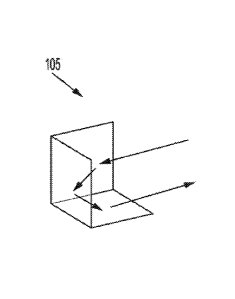
[29] Figure 1A is a diagram of a corner cube 105, according to some
embodiments. A corner cube is a highly efficient metallic retroreflection
structure.
By connecting two (or three) metallic plates at right angles, one forms a
reflection
structure where the incoming wave is reflected two (or three) times and
achieves
retroreflection. Theoretical and experimental works show that the corner cube
provides efficient retroreflection with incident angles in the range of 15 ,
where a
"normal" incidence angle is 0 . Corner cubes are large structures, with a
depth that is
appreciable compared to the size of the aperture, and do not support
retroreflection
beyond a maximum angle of 45 . Some corner cubes alter the polarization of the
4
CA 03075970 2020-03-16
WO 2019/082164 PCT/IB2018/058408
incident EM wave. Corner cube dimensions are reduced by building a sheet of
corner
cubes using a 2-dimensional (2D) array of small trihedral corner cubes, while
having
appreciable retroreflection with incident angles in the range of 30 . Even
low-
dimension corner cubes are not efficient at high-incident angle (e.g., large
oblique
angle) EM waves.
[30] Another class of retroreflectors involves dielectric and/or plasmonic
materials. For a random array of spherical (or near-spherical) scatterers,
coherent back
scattering occurs to strengthen retroreflection. Under favorable conditions, a
retroreflection strength as high as 40% has been observed. A similar effect
occurs for
random rough surfaces. Surfaces with random arrays of spherical or near
spherical
reflectors, or randomly rough surfaces, encourage multiple scattering, and
thereby
strengthen the retroreflected wave component which achieves phase-alignment
across
multiple paths.
[31] Figure 1B is a diagram of a cat's-eye retroreflector 110, according to
some
embodiments. A cat's eye retroreflector is a convex dielectric lens placed one
focal
length away from a (ideally parabolic) mirror. Cat's-eye retroreflectors have
a depth
that is comparable to the lateral size of the retroreflector. Because the
incident EM
wave is focused on a considerably smaller area at the location of the mirror,
a cat's-
eye retroreflector is useful for performing switching and encoding on an
electromagnetic signal. Some embodiments of a cat's-eye retroreflector with a
multistage lens have achieved highly-efficient retroreflection across 15 of
incident
angle range. Some embodiments of a cat's-eye retroreflector have an array of
micro-
lenses and micromirrors and, while having a low profile, achieve efficient
retroreflection across an incident angular range of 30 .
[32] Figure 1C is a diagram of a Luneberg lens retroreflector 115,
according to
some embodiments. A Luneberg lens retroreflector replaces a convex lens of the
cat's-
eye retroreflector with a lens-mirror spacing of a Luneburg lens, one arrives
at the
Luneburg lens retroreflector. Some embodiments of Luneberg lens
retroreflectors
have efficient retroreflection across an incident angular range of about 50 .
A
Luneburg lens retroreflector is limited by its large size, heavy weight and
relatively
expensive fabrication. More exotic metallodielectric retroreflectors have been
proposed.
CA 03075970 2020-03-16
WO 2019/082164 PCT/IB2018/058408
[33] Figure 1D is a diagram of an Eaton lens 120, according to some
embodiments. Eaton lens 120 performs retroreflection by trapping EM waves
within
the structure of the reflector and uses a high degree of internal reflection
to redirect
the EM waves through the lens from an input end to an output end, and from
thence
toward a target in line with the output end of the lens. Further examples of
metallodielectric retroreflectors include retro-reflection super-scatterer
implemented
through the transformation optics approach, and a plasmonic superscatterer, a
superdirective small antenna, impedance matched by metal and dielectric shells
of
precise thickness. Such retroreflectors involve high precision manufacturing
and
materials controls.
[34] Figure 1E is a diagram of a Van Atta array retroreflector 125,
according to
some embodiments. The Van Atta array is a practical and low profile wide angle
retroreflector for RF electromagnetic waves, with a surface designed to
efficiently
couple to the incident and reflected waves, where crossed transmission-line
connections between antenna areas_reverse the phase front on the surface of
the
retroreflector. Thus together, the Van Atta array antennas and their
connections
reverse the phase front along the surface of the retroreflector to achieve
retroreflection. Van Atta arrays work in 1D and 2D configurations, and on both
planar
and curved surfaces, and for a wide incident angular range of over 60 .
However,
the Van Atta array relies on the near-resonant operation of antenna elements.
Hence
the operation bandwidth of a Van Atta array is limited by the antenna
elements, and
the incident angular range of retroreflected EM waves is regulated by the
element
factor. The element factor is the electric field pattern produced by a single
cell
(element) which defines the angular base band and angular bandwidth for the
reflective response. In the example above, for the Van Atta array, the angular
base
band ranges from about -60 to about +60 , and has a narrow angular bandwidth
of
about 5 at 0 or 1 at +60 or -60 . Similarly, extension of Van Atta array
retroreflection beyond the mm-wave regime is difficult because of limitations
of the
antenna elements and the transmission lines between antenna elements.
Additionally,
the complexity of routing between antennas rapidly increases with increasing
antenna
array size. This makes the Van Atta array impractical for a retroreflector
with an
aperture length of several wavelengths and beyond.
6
CA 03075970 2020-03-16
WO 2019/082164 PCT/IB2018/058408
[35] Figures 1F-1H are examples of gratings that are configured to interact
with
incident EM waves. Figure 1F is an echellete grating 130, according to some
embodiments of the present disclosure. Echellete grating 130 has peaks 132 and
troughs 134, with a period 136 between adjacent peaks 132 and/or adjacent
troughs
134 of the echellete grating 130. Figure 1G is a groove grating 140, according
to some
embodiments of the present disclosure. Groove grating 140 includes peaks 142
and
troughs 144 configured to interact with incoming electromagnetic (EM)
radiation (EM
waves) and to manipulate the reflection of an incident EM wave according to
the
pattern and dimensions of the groove peaks and troughs. Figure 1H is a strip
grating
150 according to some embodiments of the present disclosure. Strip grating 150
includes a backing metallic layer 152, on which a dielectric layer 154 rests,
with
metallic islands 156 on the top surface of the dielectric layer (the side
opposite the
backing metallic layer 152). The pattern of metallic islands 156 on the top
surface
158 of the dielectric 154 regulates the reflection characteristics of incident
EM wave.
[36] Figure 11 is a top-view of a metasurface 160 configured to reflect
incident
EM waves from the metasurface 160. Metasurface 160 includes a periodic array
162
of surface structures 164 configured to interact with incident EM waves and to
manipulate the EM waves upon reflection from the metasurface 160. In
metasurface
160, each periodic array 162 includes a set of non-repeating surface
structures. In
some embodiments of metasurfaces, the periodic array includes some repeated
surface
structures, separated across the metasurface. In some embodiments of
metasurfaces,
the periodic array includes line structures that extend upward from a base
layer of the
metasurface. In some embodiments, of metasurfaces, the periodic array includes
holes
(slots, lines, grooves, and so forth) that extend into the metasurface base
layer. In
some embodiments, the metasurface includes a combination of line structures
that
extend upward from a base layer of the metasurface, and a set of holes that
extend into
the metasurface base layer. In some embodiments, the metasurface is a single
material. In some embodiments, the metasurface is a stack of materials, with
features
of one material covered in (or extending into) another material. In some
embodiments,
the period array 162 is longer in a first direction 163 on the metasurface
than in a
second direction 161 of the metasurface.
7
CA 03075970 2020-03-16
WO 2019/082164 PCT/IB2018/058408
[37] Metasurfaces such as metasurface 160 are versatile tools in EM wave
manipulation. By tuning the surface impedance as a function of position across
the
metasurface, metasurfaces perform wave operations which modify the amplitude,
phase, polarization and propagation direction of an incident wave are
performed in a
passive manner. Passive wave operations are performed as an incident EM wave
strikes and reflects from a metasurface, without any active EM wave generation
to
interact with the incident or reflected wave. Metasurfaces with linear phase
variants
represent low profile and cost-effective structures. The angle of reflection
from a
metasurface is regulated according to the structure of (or structural elements
in) the
metasurface. Metasurfaces, being inherently two-dimensional, provide more
freedom
in waveform manipulation than gratings, which are inherently one-dimensional.
Until
the present disclosure, metasurfaces have featured finely discretized surface
impedance profiles implemented by element cells of size A/8 (e.g., one eighth
of a
wavelength) or smaller. For such finely discretized surface impedance profiles
to
interact with EM waves having higher frequencies involves high-precision
fabrication.
Metasurfaces with highly-precise structural elements are generally more
expensive to
manufacture, less robust after manufacture, and/or difficult or impossible to
scale to
shorter wavelengths. As of this disclosure, there is little information about
near-
grazing (i.e., large incident angle) metasurface operation, including little
or no
information about power efficiency of near-grazing metasurface operations.
[38] The present disclosure describes the design and manufacture of
embodiments
of metasurfaces with near-grazing angle retroreflection for both TE and TM
polarized
EM waves. A TE polarized EM wave has the electric field vector perpendicular
to the
plane of incidence, and a TM polarized EM wave has the magnetic field vector
perpendicular to the plane of incidence. In some embodiments, metasurfaces
with
near-grazing retroreflection include a subwavelength array of rods (for TE
waves) and
/ or slots (for TM waves) backed by a ground plane. In some embodiments of
metasurfaces described herein, the metasurface includes a grating with a(n
ultra-
coarse) discretization of two cells per grating period. Embodiments of
metasurfaces
with two cells per grating period alleviate, to a large degree, the need for
small
features. Such metasurfaces also present opportunities to design and
manufacture
metasurfaces with highly reflection efficiency, robust surfaces, cost
effectiveness, and
ease of scaling to mm-wavelengths and THz frequencies. The remainder of the
present
8
CA 03075970 2020-03-16
WO 2019/082164 PCT/IB2018/058408
disclosure presents a metasurface design methodology and describes embodiments
of
metasurfaces and full-wave simulation results for TE and TM retroreflection
metasurfaces. For embodiments of TM-reflective metasurfaces, the present
disclosure
examines origins of spurious reflections not observed for embodiments of TE-
reflective metasurfaces. The present disclosure also includes methods and
results of
monostatic and bi-static radiation cross section (RCS) experiments that
validate the
metasurface design methodology presented herein. Diagrams of RCS measurements
have nodes that correspond to the intensity of an EM wave that is reflected
from the
metasurface. Some nodes correspond to specular reflection, some nodes
correspond
to retroreflection, and some nodes correspond to spurious reflection in a
direction
other than the incident angle 0, or the reflected angle Or or a negative of
the reflection
angle -Or.
[39] The
present disclosure discusses the reflective properties of embodiments of
a periodic metasurface with aggressively discretization for reflecting both TE
and TM
waves. In some embodiments, the reflective metasurfaces includes two cells per
grating period to perform the EM wave reflection. In some embodiments, the
reflection of TE and TM waves is retroreflection of an incident EM wave. In
some
embodiments, the reflection is at an angle that corresponds to neither a
retroreflection
angle nor to a specular reflection angle.
Simplification of a retroreflective
metasurface by using larger feature sizes and more aggressive discretization
allows
for easier, lower cost design and fabrication of a metasurface. Simulation and
measurement of a binary Huygens' metasurface, discretized to have two elements
per
unit cell, is described below. In some embodiments, a metasurface has a number
of
cell elements that is greater than two elements per unit cell, according to an
incident
EM wave desired to be reflected from the metasurface. According to some
embodiments, the upper limit of the number of elements in a unit cell is
regulated by
the size or area of a desired reflective metasurface and the configuration of
EM wave
reflection intended form the reflective metasurface. Dimensions of a
reflective
element of a metasurface unit cell are governed by the wavelength of the
incident EM
wave. A number of reflective elements in a metasurface unit cell is not so
large that
the reflective elements no longer serve to reflect the incident EM wave. In
an
embodiment of a metasurface, the simulated and measured metasurface
retroreflects
an incident plane wave at 82.87 . In some embodiments, the simulated results
for a
9
CA 03075970 2020-03-16
WO 2019/082164 PCT/IB2018/058408
2D infinite structure have a reflection power efficiency of 94% for TE
polarization,
and 99% for TM polarization. In some embodiments, measured retroreflection has
a
reflection power efficiency of 93% for both TE and TM polarizations. In some
embodiments, the metasurface is configured to reflect an incident plane wave,
having
an incident angle 0, at a predetermined reflection angle Or where 0, = Or
(e.g.,
retroflection). According to some embodiments, the incident angle ranges as:
90 >
0, > 0 . In some embodiments, a metasurface is configured to reflect an
incident plane
wave at a predetermined reflection angle Or , where Or 0, and Or - 0, (e.g.,
neither
retroreflection nor specular reflection). A range of reflection angles for a
reflected
EM wave, from an incident EM wave with an incident angle 01, as given above,
ranges
as 89.5 > Or > 0 . Some embodiments of controlled-reflection metasurfaces are
configured to retroreflect incident one or more incident EM waves at one or
more
arbitrary reflection angles. In some embodiments, the reflection of an EM wave
is
adjusted to reflect either TE or TM waves. In some embodiments, the reflection
of an
EM wave is adjusted to reflect both TE and TM waves.
[40] METASURFACE DESIGN METHODOLOGY
[41] Metasurface design as presented herein is performed using a surface
impedance approach. To design a reflective metasurface, one first begins by
determining the surface impedance (and reflection coefficient) profile of the
reflective
metasurface, followed by examining the effects of discretization on the
performance
of the metasurface.
[42] A. Surface Impedance Analysis
CA 03075970 2020-03-16
WO 2019/082164 PCT/IB2018/058408
[43] Figure 2A is a diagram 200 of a single plane TM wave 202 reflection in
the
yz plane, off a metasurface 204 at z = 0. TM wave 202 has an incident
electrical
component Ei 206 that is parallel to the metasurface, and the incident
magnetic
component Hi 208 that is perpendicular to the metasurface. Similarly, TM plane
wave
202 has the reflected electrical component 210 Ei is parallel to the
metasurface and
the reflected magnetic component 212 Hi is perpendicular to the metasurface.
Incident
angle 0, 214 of TM wave 202 is the same as reflection angle Or 216, indicative
of
specular reflection of the incident EM wave from metasurface 204. Incident
angle Oi
214 and reflected angle Or 216 are both positive angles, measured from the z-
axis in
the yz-plane. k, 218 is the incident wave number (vector), and kr 220 is the
reflected
wave number (vector).
[44] Figure 2B is a diagram 240 of a single plane TE wave 242 reflection in
the
yz plane, off a metasurface 244 at z = 0. TE wave 242 has an incident
electrical
component Ei 246 that is perpendicular to the metasurface and an incident
magnetic
component Hi 248 that is parallel to the metasurface. Similarly, TE plane wave
202
has a reflected electrical component 250 Ei that is perpendicular to the
metasurface
and a reflected magnetic component 252 Hi that is parallel to the metasurface.
Incident
angle 0, 254 of TE wave 242 is the same as reflection angle Or 256, indicative
of
specular reflection of the incident EM wave from metasurface 244. Incident
angle 0,
254 and reflected angle Or 256 are both positive angles, measured from the z-
axis in
the yz-plane. k, 258 is the incident EM wave number (vector) and kr 260 is the
reflected wave number (vector).
[45] In some embodiments, the incident angle of the EM wave is the same as
the
reflected angle of the reflected EM wave, and the reflection is called
specular
reflection. When an EM wave retroreflects back along the incident direction to
an EM
source, the reflected angle Or is negative because the reflected angle is
measured in an
opposite rotational direction from the z-axis [Or= ¨Of] in the yz-plane. Thus,
for "pure"
retroreflection, directly back to an EM wave source, the reflection angle is a
negative
of the incidence angle of the EM wave. Plain metal surfaces exhibit specular
reflection. Some embodiments of metasurfaces described herein exhibit both
specular
reflection, and retroreflection (e.g., major nodes of reflected signal are
present in a
RCS measurement of a metasurface, as with Figures 10A-C, below). The
reflective
11
CA 03075970 2020-03-16
WO 2019/082164 PCT/IB2018/058408
characteristics of the metasurface are related to the geometry and physical
composition of the metasurface, which determine the angle at which an incident
EM
wave, or incident radiation, reflects from the metasurface. Some metasurfaces
described herein are configured to reflect at a single incident angle (or, a
window of
angles around a main incident angle). Some metasurfaces described herein are
configured to reflect at multiple main incident angles, according to layouts
and
compositions of the elements in unit cells of the metasurface. In some
instances,
metasurfaces described herein are configured to reflect EM waves approaching a
metasurface at multiple incident angles, away from the metasurface at a single
reflection angle, according to some embodiments.
[46] Equations (1)-(14) describe the method of analyzing surface impedance
using TM incident polarization, to make metasurfaces with controlled
reflection
and/or retroreflection. In Figure 2A, electric (Ei) and magnetic (Hi) portions
of an
incident plane wave are described by equations 1 and 2, and the electric (Er)
and
magnetic (Hr) portions of a reflected plane wave are described by equations 3
and 4,
below:
= Eioexp(¨jko (sin Oi y ¨ cos Oi z)) = (cos O 9 + sin Oi 2)
Equation
(1),
Eio
Hi = ¨ exp(¨jko (sin Oiy ¨ cos 0 iz))2
Equation
(2),
Er = Eroexp(¨jko (sin Or y ¨ cos Or z)) = (cos Or 9 + sin Or 2)
Equation
(3),
and
Ero
Hr = ¨ exp(¨jko (sin Ory ¨ cos Orz))2
Equation
(4),
where:
Oi = is the angle of incidence of the incident EM waveform,
12
CA 03075970 2020-03-16
WO 2019/082164 PCT/IB2018/058408
Or = is the angle of reflection of the EM waveform,
Et() = is the incident electric field,
Er0 = is the reflected electric field,
y = is the y component in the x-y-z coordinate system,
z = is the z component in the x-y-z coordinate system,
j = is an imaginary number,
= is the total energy density used in the conversion from the magnetic field
to
electric field in free space,
ko = is the incident wave number (vector),
= is unit vector component in the x direction,
= is unit vector component in the y direction, and
2 = is unit vector component in the z direction
[47] Here ko = 2p= Ao is the spatial frequency the wave and /0 is the free-
space
wavelength. f is a constant phase offset between the incident and reflected
waves at y
= 0, which remains arbitrary for the moment. The incident and reflected
electric (El,tan
, Er,tan) and magnetic (HI,tan , Hr,tan) fields tangential to the surface (at
z=0+) are hence
described as follows:
Ei,tan = E0 cos Oiexp(¨jko sin Oi y)9
Equation
(5)
Eio
H i,tan = ¨ exp (-11(0 sin Oi y)2
Equation
(6),
Er,tan = Ero cos Or exp(¨jko sin Or y + 0)9
Equation
(7),
and
13
CA 03075970 2020-03-16
WO 2019/082164 PCT/IB2018/058408
Hr,tan = ¨ exp(¨jko sin Or y + 0)2 Equation
(8).
The two relationships introduced hereinafter simplify the derivation that
follows. In
equation (9), below:
A.1)(y) = ko (sin er ¨ sin 03y + .1) Equation
(9)
A is defined as the phase difference between the incident and reflected plane
waves.
Equation (10), below,
,I cos ei
Ero = ¨cos Or Eio Equation
(10)
relates the incident and reflected plane wave amplitudes for reflection
metasurfaces.
Equations (9) and (10) are used to calculate the surface impedance as a
function of a
location on the metasurface. The surface impedance of a metasurface is used to
generate a desired reflection based upon the prescribed incidence of an EM
wave, as
given below in Equation (11):
Etan'5) (Ei,tan+Entan)'5)
Zs,Tm = =
Htanf (11i,tan+Hr,tan)'2
cos OiVcos Or¨cos OrVcos Otexp(¨jAcKy))
= Equation
Vcos Or+Vcos Otexp(¨ jAcD(y))
(11).
[48] For the case of retroreflection, Or= ¨0,
cost), = cosOi. Redefining 0 =10,1=
119,1, Equation (11) becomes:
14
CA 03075970 2020-03-16
WO 2019/082164
PCT/IB2018/058408
e --Atm
.4y m = q 1
cose _____________________
\ +e-jtvtly)
jZosrm tan _______________ ,
,1
Equation (12),
where Zo,Tm=r7cos0 is the wave impedance for the incident and reflected waves
in TM
polarization
[49] In some embodiments, a description of reflection coefficients is
preferable
to a description of surface impedances In an embodiment of single plane wave
retroreflection, the reflection coefficient is described by Equation (13),
below:
Z-1 ¨ 27 } T 401
:
4,11-f --1-4-J,rm Equation (13)
[50] A corresponding relationship for the TE polarization is found by
following
a procedure similar to the procedure of Equations (1)-(13) For the TE-
polarized
single wave reflection scenario described by FIG 2B, the surface impedance is
given
in Equation (14):
\l¨cos
=
,
Vox ei cos 9, vicosei
Equation (14)
[51] Equation (14) reduces to Equation (15) when describing
retroreflection:
,(A(Df v)
E 14,T E COI
Equation (15),
where ZO,TE = q/cos0 is the wave impedance for TE-polarized incident and
reflected
waves The reflection coefficient which corresponds to the surface impedance of
equation (13), above, is given in Equation (16):
27.? TE 2:0 T
17TE CA" =
:4,2E + E
Equation (16)
CA 03075970 2020-03-16
WO 2019/082164 PCT/IB2018/058408
[52] Relationships akin to Equations (11) and (14) have been derived, to
various
degrees of generality. In some embodiments, a coefficient profile of a
metasurface is
correctly approximated by using equations (12) and (16) for a linear phase
gradient.
The preceding analysis shows, with the full rigor of Maxwell's equations, that
retroreflection of the full power of an incident plane wave, at any incidence
angle, and
with either TM or TE polarization, is possible.
Moreover, such full power
retroreflection is achievable using an aptly designed passive metasurface with
surface
impedances described by equations (11) and (14), or equivalently with
reflection
coefficients described by (12) and (16).
[53] B. Discretization and Retroreflection Metasurfaces
[54] Implementation of a discretized metasurface, having subwavelength-
sized
cells, each of which is implemented to achieved the desired electromagnetic
property
(e.g. surface susceptibility or surface impedance, is more facile than the
implementation of a continuous metasurface), and coarser discretization
(having cells
of greater-than subwavelength-sized cells), is possible for selected
reflection surfaces.
Coarse discretization benefits metasurface design by, first, reducing the
mutual
coupling between metasurface elements, and second, by relaxing the tolerances
of a
retroreflective metasurface, allowing for cost-effective (e.g., less
expensive) and
robust metasurface fabrication for incident EM wave well into the mm-wave
frequencies. A brief discussion of design of an aggressively discretized
retroreflection
metasurface is provided below.
[55] Figure 3A is a spectral diagram 300 of the transformation of a plane
wave's
transverse (y-directed) wave vector 302, as the plane wave is reflected from a
periodic
metasurface. Arrows indicate the spatial frequencies of possible spectral
components,
but arrow lengths do not reflect the relative amplitudes of these components.
[56] In Figure 3B, is a diagram 320 spatial frequencies 322, 324, 326, 328,
and
330 of reflections of an incident transverse (y-directed) plane wave vector
302 from a
retroreflection metasurface. These spatial frequencies map straightforwardly
into the
angular domain through Equation (17)
16
CA 03075970 2020-03-16
WO 2019/082164 PCT/IB2018/058408
= fork <k
y
Equation (17),
where 0 = is the angle of incident,
ko = is the incident wave number (vector), and
ky = is the component of the wave number (vector) in they direction.
[57] Figure 3C is a diagram 340 of the spectral components 342, 344, 346,
and
348 of reflected wave vector 302. Note that the arrows that represent the
spectral
components do not represent the amplitudes or phases of the spectral
components. As
seen, the spectral components 342-348 represent a series of diffraction orders
which
reflect in different directions. The transverse spatial frequencies of
diffracted orders
are described by Equation (18):
2n
kmy = kiy + mkg = kiy + m¨ Equation (18),
A9
where:
kmy = represents the diffraction order wave number (vector),
k,y represents the incident wave number (vector) in the y direction,
m represents the diffraction order number,
kg represents the spatial frequency of the metasurface, and
Ag represents the period of the metasurface.
[58] To generate a retroreflection metasurface, the m=-1 diffraction order
is
tuned into the retroreflection order by choosing Ag appropriately:
2n
kry = k = ¨ ¨ = ¨kiy
IY A
Ao
,v = 2 sin 19
¨ Equation (19)
i
17
CA 03075970 2020-03-16
WO 2019/082164
PCT/IB2018/058408
[59] For a metasurface which implements the surface impedance profile
described
by Equations (11) and (14), power diffraction increases for the
retroreflection mode
and vanishes for other propagating modes.
[60] With Ag, and thereby kg, fixed to achieve retroreflection at a
predefined
angle, there exists a fixed number of reflected propagation waves, which are
described
by:
N=
Equation (20)
where 11 is the ceiling (round up) operator,
ko = is the incident wave number (vector), and
kg = represents the spatial frequency of the metasurface.
[61] In some embodiments, increasing metasurface discretization involves
reducing the number of cells N of the metasurface period. Maximizing
metasurface
discretization involves reducing the number of cells N cells per metasurface
period as
much as possible, while still providing sufficient degrees of freedom to tune
the
amplitude and phase of each diffraction order. The degree of such
maximization, and
the number N of cells per metasurface period to achieve the maximization, is
demonstrable using Fourier analysis. For a retroreflector, the number of cells
N for
metasurface discretization is simplified to:
kz-)
N = 2 x =
kõ
_
Equation (21),
where 1:1 is the rounding operator. Combining equations (17), (19), and (21),
for a
sufficiently large angle incidence, the number of cells per metasurface period
is found
to be:
18
CA 03075970 2020-03-16
WO 2019/082164 PCT/IB2018/058408
2
> 19S k ¨k.;) ¨ 2
Equation
(22)
[62] Hence for angles of incidence beyond 19.5 , the retroreflection
metasurface
can be most aggressively discretized to have only two cells per grating
period. A case
for minimum discretization concurs with the article published by A. Hessel, J.
Schmoys, and D. Y. Tseng, Bragg-angle blazing of diffraction gratings, J. Opt.
Soc.
Am., vol. 65, no. 4, pp. 380-383, Apr 1975. Application of Equations (13) and
(16)
shows that the two cells exhibits near-full reflection amplitude (e.g.,
"perfect"
reflection, or reflection of nearly 100% of the incident EM waveform) and 180
relative phase shift. A description of the design and simulation of TE and TM
metasurfaces which achieve near-full reflection amplitude and 180 relative
phase
shift follows below.
[63] METASURFACE SIMULATION AND DESIGN
[64] Figure 4A is a diagram of a retroreflection model 400 from a
metasurface
402 with incident 404 and reflected 406A, 406B EM waves, according to some
embodiments. Reflected EM wave 406A is a retroreflected EM wave, returning
along
the incident direction of incident EM wave 404. Reflected EM wave 406B is a
specular reflected EM wave. Incident angle 0, 408 is measured from a reference
line
410 normal to a top surface of metasurface 402. In retroreflection, when
incident
angle 0, 408 is positive (0, >0) and is on one side of reference line 410,
specular
reflected EM wave 406B has a reflection angle Or,spec 409 that is positive
(0r,spec >0)
on the opposite side of reference line 410. Thus, reflected wave 406A has a
reflection
angle (0r,retro > -0,). Incident and reflected EM waves shown in
retroreflection model
400 are contained in a reflection plane 412 described by the yz plane (see z-
axis 421
and y-axis 422), with the x-axis 423 being perpendicular to reflection plane
412.
[65] Whereas a smooth surface reflects incident EM waves 404 in the
specular
direction (see 406B), a controlled-reflection metasurface is configured to
reflect light
in a direction other than the specular direction. Some embodiments of
controlled-
reflection metasurfaces reflect incident EM waves (see incident wave 404) in
the retro
direction (see, e.g., reflected EM wave 406A). Some embodiments of controlled-
19
CA 03075970 2020-03-16
WO 2019/082164 PCT/IB2018/058408
reflection metasurfaces reflect incident EM waves the retro direction, back
toward an
EM wave source (not shown). For a TE polarized wave, the E-field points to the
x-
direction; for a TM polarized wave, the H-field points to the x-direction. In
the present
disclosure, design of a metasurface that emanates two diffraction orders ¨ the
specular (m = 0) and retroreflection (m = ¨1) orders, is presented. By
appropriate
metasurface design it is possible to significantly suppress specular
reflection and
hence create an efficient retroreflector. The present disclosure discusses a
24GHz
incident wave impinging on a metasurface at a near-grazing incident angle of
0, =
82.87 . It is noteworthy that the example incident angle and EM wave frequency
are
merely intended for clarity of discussion of the principles involved with
designing and
making controlled-reflection waves. Other incident angles and wave frequencies
are
envisioned within the scope of the present disclosure. Substituting the
incident angle
and EM wave frequency into equation (19), the metasurface period Ag is found
to be:
6,30nun Equation
(23)
[66] The unit cell size Uy is determined by Equation (24) for a metasurface
period
discretized into two cells:
15mm.
Equation
(24).
[67] Figure 4B is a flow diagram of a method 440 of designing and making a
metasurface with controlled-reflection characteristics, according to some
embodiments of the present disclosure. A metasurface design is determined by
performing an operation 442 in which the incident angle of the EM waves that
are to
reflect from a metasurface is selected to determine the metasurface
configuration. In
some embodiments, the incident angle of EM waves to reflect from the
metasurface
ranges from about 10 to about 88 . In some embodiments, the incident angle of
EM
waves is greater than 75 and less than 90 .
[68] Method 440 proceeds with operation 444, in which at least one
reflection
angle is selected for the EM waves incident to the metasurface. In some
embodiments,
CA 03075970 2020-03-16
WO 2019/082164 PCT/IB2018/058408
the reflection angle is negative, and the EM wave reflects generally back
toward the
EM wave source or horn. In some embodiments, the reflection angle is equal to
the
negative incidence angle of the EM wave (e.g., Or = -Of). In some embodiments,
the
reflection angle is positive, but has a different magnitude than the incidence
angle.
[69] Method 440 proceeds with an optional operation 446, in which the
metasurface is divided into regions according to a number of incident angles
and
reflected angles selected in operations 442 and 444, previously.
[70] Method 440 proceeds with operation 448, in which the polarizations of
the
EM waves to reflect off the metasurface are selected. In some embodiments, the
metasurface is configured to controllably-reflect TE-polarized EM waves. In
some
embodiments, the metasurface is configured to controllably-reflect TM-
polarized EM
waves. In some embodiments, the metasurface is configured to controllably-
reflect
both TE- and TM-polarized EM waves.
[71] When a TE-polarized incident EM wave is selected for controlled
reflection,
the method 440 proceeds with operation 450, wherein the shape of a conductive
element of a TE-reflective metasurface is determined. Operations associated
with
determining a shape of a TE-reflective metasurface are described hereinabove,
and are
described further by equations (1)-(16), associated with the determining the
dimensions of both a unit cell of a metasurface and shape / dimensions of
conductive
elements thereon.
[72] When a TM-polarized incident EM wave is selected for controlled
reflection,
the method 440 proceeds with operation 452, wherein the shape of a conductive
element of a TM-reflective metasurface is determined. Operations associated
with
determining the shape of a TM-reflective metasurface are described
hereinabove, and
are described further by equations (1)-(16), associated with the determining
the
dimensions of both a unit cell of a metasurface and shape / dimensions of
conductive
elements thereon.
[73] Method 440 proceeds with operation 454, wherein it is determined
whether
all regions and all polarizations, as determined in operations 442-446, have
been
evaluated to determine the metasurface design or layout. When not all regions
or
polarizations have been evaluated, the method proceeds to operation 448.
21
CA 03075970 2020-03-16
WO 2019/082164 PCT/IB2018/058408
[74] Method 440 proceeds with operation 456, wherein the metasurface
elements
are combined into a metasurface layout by region, in order to perform the
controlled
reflection that is sought after operations 442-446 have been completed.
According to
some embodiments, a first region of a metasurface is configured to
controllably-reflect
both the incident TE- and TM-polarized portions of an EM wave at a same
reflection
angle. In some embodiments, a first region of a metasurface is configured to
controllably-reflect both incident TE- and TM-polarized portions of an EM
wave,
where TE-polarized EM waves are reflected at a first reflection angle and TM-
polarized EM waves are reflected at a second reflection angle. In some
embodiments,
a first region of a metasurface is configured to specularly reflect one
portion (or
polarization) of an incident EM wave, and controllably-reflect a majority of
the other
portion (or polarization) of the incident EM wave. In some embodiments, a
first region
of a metasurface is configured to reflect an incident EM wave (both TE and TM
polarizations) at a first reflection angle and a second region of the
metasurface reflects
the incident EM wave (both TE and TM polarizations) at a second reflection
angle,
different from the first reflection angle. In other words, the present
disclosure
provides a methodology of designing a metasurface that allows for reflecting
portions
of more than one EM wave, at more than one incident angle, at more than one
reflection angle, and handling the TE and TM polarized portions of the more
than one
EM wave independently.
[75] Method 440 proceeds with operation 458, wherein a pattern of
conductive
(metallic) elements on a top surface of an insulating material, the pattern
corresponding to the metasurface layout, by region, formed during operation
456.
[76] In a non-limiting embodiment, a metasurface is manufactured using a
Rogers
RT/Duroid 5880 laminate board with 1/2 oz. copper cladding on both sides.
According
to some embodiments, the metasurface is constructed from an insulating
material, or
insulating substrate, or dielectric material, with a conductive ground plane
on a first,
or bottom, side of the insulating substrate, and a series of unit cells with
conductive
elements located therein on a second, or top, side of the insulating
substrate.
According to some embodiments, the insulating substrate is an insulator
material
suitable for printed circuit board or microstrip manufacturing. According to
some
embodiments, the insulating substrate is polyimide, polyethylene,
polypropylene,
22
CA 03075970 2020-03-16
WO 2019/082164 PCT/IB2018/058408
polyisocyanate, polytetrafluoroethylene (PTFE), fiberglass, or some other non-
conductive inorganic or organic material that electrically isolates the
conductive
ground plane from the conductive elements on the top of the insulating
substrate.
According to some embodiments, the conductive ground plane and the conductive
elements on the top surface of the insulating substrate are a same metal.
According
to some embodiments, the conductive ground plane and conductive elements on
the
top surface of the insulating substrate are different metals. Some embodiments
of
metasurfaces include, but are not limited to, metals such as copper, aluminum,
nickel,
silver, gold, brass, and alloys of these and other metals.
[77] A pattern of conductive or metallic elements on a top surface of an
insulating
material is formed, according to some embodiments, by masking a portion of a
blanket
metallic film on a top side of the insulating material, with a removable mask,
and
subsequently etching the conductive or metallic layer on the top side with an
acid, or
by sputtering or abrading the material away from within the openings of the
removable
mask. In some embodiments, the ground plane on the bottom side of the
insulating
material has a same composition and a same thickness as a conductive or
metallic film
on the top side of the insulating material. In some embodiments, the ground
plane is
also masked, with a blanket mask material, to protect the conductive or
metallic
material of the ground plane from the etching process that forms the pattern
of
conductive elements on the top surface of the insulating material during
operation 458.
According to some embodiments, a first region, having a first layout, and a
second
region, having a second layout, are formed in a same pattern forming
operation.
[78] TE METASURFACE ELEMENT DESIGN
[79] For the TE polarization, a reflection coefficient is implemented using
a
ground-backed dipole array. A ground-backed dipole array contains Huygens'
source
characteristics when operated in reflection mode. Further, by tuning the
length of the
dipole one can vary the phase of FTE by a phase range approaching 360 , with
minimal
loss.
[80] Figure 5A is a diagram of a metasurface unit cell 500, where the
metasurface
is TE-reflective and includes a ground-backed dipole array. Metasurface unit
cell
500 has a cell thickness 502 Sz with a unit cell length 504 Ux and a cell
width 506 U.
23
CA 03075970 2020-03-16
WO 2019/082164 PCT/IB2018/058408
The ground-backed dipole 508 has a dipole length 510 Px and a dipole width P.
According to a non-limiting embodiment, the metasurface unit cell 500 is made
on a
Rogers RT/Duroid 5880 Laminate board from Rogers Corp., with a cell thickness
Sz =
1.575mm and 1/2 oz. copper cladding. According to some embodiments, and as
described above in Equation (23), an aggressively discretized unit cell for
retroreflection of an incident a square cell profile, where Ux= Uy= 3.15mm,
and where
the ground-backed dipole has a square dipole profile Px = Py = 0.5mm.
According to
some embodiments, a ground-backed dipole is a conductive element on a top
surface
of an insulating material, as described hereinbelow, that is discontinuous
from
conductive elements in unit cells of the metasurface that adjoin the unit cell
containing
the ground-backed dipole. For example, ground-backed dipole 508 is surrounded
by
an air gap at a top surface of an insulating material, as shown in Figure 5A.
[81] Figure 5B is a diagram of a simulated RCS measurement 520 the TE
reflection coefficient FTE as a function of the dipole length for unit cell
500 described
by Figure 5A, using Ansys HFSS full-wave electromagnetic simulation. Unit cell
500
has periodic boundaries in the x and y directions, with phase shifts
corresponding to
an incident wave at 0, = ¨82.87 , a Floquet waveport from the +z boundary, but
with
a dipole length ranging from Px= 1.5mm to 3mm for simulation purposes.
Simulation
results show a phase change approaching 360 with relatively low energy loss
(less
than 5% for nearly according to the diagram 520). As noted in diagram 520,
operation
points PA = 2.16 mm and Px2 = 2.35 mm differ in phase by about 180 . Thus, PA
=
2.16 mm and Px2 = 2.35 mm are selected to be the operating points of a
retroreflection
metasurface for TE polarizations.
[82] Figure 5C is top view of an effective area or active area of a two
cell TE-
retroreflective metasurface 540, according to some embodiments. In
some
embodiments, TE-reflective metasurface element 542 has a cell length
dimensions Ux
=Uy = 3.149mm, S= 1.575mm, Py= 0.5mm, although other [see above, Figure 5A]
The dipole width Py = 1.5mm, and dipole lengths Pi = 2.16mm, Px2 = 2.35mm, are
configured to generate high-efficiency retroreflection of an incident 24 GHz
TE
polarized waveform at an incident angle of 0,= ¨82.87 .
24
CA 03075970 2020-03-16
WO 2019/082164 PCT/IB2018/058408
[83] SIMULATION OF PERIOD METASURFACES
[84] After selection of the dipole cell lengths PA and Px2, the dipoles are
placed
adjacent to each other and the scattering properties of the resultant binary
Huygens'
metasurface are simulated. Figure 5C shows a top view of one period of this
metasurface. A first simulation of a 2D infinitely periodic extension of the
metasurface
is performed using the Floquet simulation described above for the single
element
analysis. According to some embodiments, from the first simulation, the
scattered
power into the retro and specular modes to be 94% and 6% respectively. The
first
simulation demonstrates very efficient retroreflection and suppression of
specular
reflection. According to some embodiments, in a second simulation the
metasurface
is truncated to 136 cells in they-direction to simulate the scattering
characteristics of
a finite metasurface. The second simulation is periodic in the x-direction ¨
where the
fields are invariant from element to element ¨ to conserve computational
resources.
[85] Figure 6A is a diagram of a truncated (1D finite) TM retroreflection
metasurface 600 used for simulation purposes as described hereinafter in the
discussion of Figures 6B-6C according to some embodiments. Metasurface 600
includes a substrate 602 and a plurality of ground-backed dipoles 604 arranged
on /
embedded in a top surface 606 of substrate 602. As
part of the simulation, the
metasurface 600 is surrounded by an air gap of A0/2 in the x- and z-
directions to
simulate radiation boundaries using perfectly matched layers.
[86] Figure 6B is a diagram 620 a simulated bistatic radiation cross
section (a
bistatic RCS) measurement of the truncated TM retroreflection metasurface 600
of
Figure 6A, in the yo = 90 plane (yz-plane) upon illumination of a plane wave
at 82.87 ,
according to some embodiments. Diagram 620 exhibits a node 622 associated with
strong retroreflection, along with a node 624 associated with weak specular
reflection.
[87] Figure 6C is a comparison diagram of the monostatic RCS 640 in the
4:1) =
90 plane (yz-plane) of two surfaces. The dashed line indicates the measured
signal
642 associated with the power of a EM wave reflected from a copper plate.
Peaks 644
and 646A-B are associated with the power of an EM wave reflected from a
controlled-
reflection metasurface, according to some embodiments. To clarify the method
of
measuring signal strengths shown in Figure 6C, refer to Figure 7, a non-
limiting
CA 03075970 2020-03-16
WO 2019/082164 PCT/IB2018/058408
embodiment of an RCS measurement apparatus 700. In Figure 7, an emitter or
horn
704 emits an EM wave 702 that strikes metasurface 710 and reflects as a
reflected EM
wave 706 at an illumination angle (q) 714. Effective aperture 712 is
calculated by
multiplying the area of the metasurface 710 by the illumination angle (q) 714
that the
horn, or emitter, makes with the normal of the metasurface. In some
embodiments of
RCS measurements, the horn 704 is configured to emit a TM polarized waveform.
In
some embodiments of RCS measurements, the horn 704 is configured to emit a TE
polarized waveform. The radiation (or reflection) cross section of a
metasurface is
determined by emitting recording the strength of the reflected EM wave 706 as
a
function of the illumination angle 714. The size of an effective aperture 712
scales
with cos0, and the radiation cross section of metasurface 710 scales with
cos20.
Because a metal plate illuminated from broadside (e.g., the incident angle is
0 ),
reflects with 100% aperture efficiency, the monostatic RCS of a copper (or
metallic)
plate provides a reference for evaluating metasurface reflection efficiency
after
accounting for the size of the aperture. In a non-limiting embodiment, at an
incident
angle of 82 , a binary Huygens' metasurface achieves an RCS of -0.3dB
compared
to a copper plate, equivalent to an aperture efficiency of 93%. Thus,
efficient
retroreflection is achievable at and/or near the angle of designed
retroreflection.
[88] TM METASURFACE ELEMENT DESIGN
[89] Metasurfaces that exhibit controlled reflection of TM-polarized
waveforms
are designed in a manner similar to that described previously for incident TM
waveforms, but with a different metasurface element. At near-grazing angles,
the
electric field component of a TM-polarized wave points predominantly in the z-
(vertical) direction with respect to the metasurface. Thus, the electric field
component
of a TM-polarized waveform couples ineffectively to a metallic dipole strip
elements
on the metasurface. Instead, an array of slots is used to couple to the
magnetic field
component of the TM-polarized wave, the Babinet's equivalent to the dipole
array of
Figure 6A.
[90] Figure 8A is a diagram of a unit cell 800 of a metasurface 801,
according to
some embodiments. In a non-limiting embodiment, metasurface 801 is a TM-
reflective metasurface with a thickness Sz 802 with a unit cell length Ux 804
and a cell
width Uy 806. In unit cell 800, a cell element that interacts with an incident
TM-
26
CA 03075970 2020-03-16
WO 2019/082164 PCT/IB2018/058408
polarized EM waveform is slot 808 having a slot length Px 810 and a slot width
Py 812.
In some embodiments, thickness Sz = 3.175mm (125 mil). In some embodiments,
the
periodicity of the cell is the same as the periodicity of the TE counterpart
discussed
previously (Ux=Uy = 3.149mm).
[91] By adjusting the length of the dipole Px, coupling dynamic between the
ground-backed slot array and the incoming/outgoing waves is adjusted, which in
turn
adjusts the reflection coefficient F Till of the metasurface. By adjusting the
reflection
coefficient of a metasurface, the relationship between the incident angle and
reflected
angle of an EM waveform is adjusted in different embodiments of controlled
reflection
/ retroreflective metasurfaces.
[92] Figure 8B is a diagram 820 of simulated reflection coefficient F Till
of a
metasurface with a slot array, as a function of the dipole length Px ranging
from 0 to
3.149 mm (the periodicity of the unit cell). Simulations of metasurface
performance
were performed using the Floquet formulation as previously explained for a TE-
polarized metasurface. As can be observed, the reflection coefficient F Till
attains near-
unity magnitude, but the phase variation of the reflected EM waveform covers
over
190 , which is a notable decrease from the near 360 phase range obtained from
the
TE counterpart. The decrease in phase variation of reflected EM waveforms is
due, in
large part, to the fact that by transforming the metasurface from TE to TM
operation
(controlled reflection / retroreflection), the metasurface retained the
original substrate
dielectric and the ground plane, whereas in a true Babinet's equivalent the
original
substrate dielectric and ground plane would be replaced with a material of
greater
magnetic permeability and a magnetic conductor. For diagram 820 with a less-
effective Babinet's equivalent, the reflection response shown is sufficient to
perform
retroreflection and demonstrate principles of a metasurface configured for
controlled
reflection of a TM-polarized waveform. Based on diagram 820, initial operation
points Pi = 0.8mm and Px2= 3.149mm are selected to perform a two-cell
simulation
described hereinbelow by Figure 8C and supporting sections of the present
disclosure
for some embodiments of metasurfaces designed for TM-polarized waveforms.
Despite the specific dimensions of metasurface 801, the unit cell and slot
dimensions
used therein are not intended to be limiting to the scope of the present
disclosure. The
present embodiments addresses all embodiments of passive controlled-reflection
27
CA 03075970 2020-03-16
WO 2019/082164 PCT/IB2018/058408
and/or retroreflecting metasurfaces with ground-backed dipoles and arrays of
slots,
for all periodicities and unit cell dimensions, and for all dipole and slot
dimensions
within the unit cells of the controlled-reflection / retroreflective
metasurfaces.
[93] Figure 8C is a top view of a non-limiting embodiment of a metasurface
unit
cell 840 used for Floquet simulation to give scattering parameters for
embodiments of
a 2D infinite extension of the binary Huyugens' metasurface. Metasurface unit
cell
840 is a TM-reflective element 842 with a cell length Ux 843, an cell width Uy
841,
and a dipole 844 with a dipole length Px] 850 and a dipole width Pyi 852.
Element 842
further has slot 846 with slot length Px2 854 and a slot width Py2 856. In
metasurface
unit cell 840, cell width 841 is 3.149mm. In some embodiments, the unit cell
length
ranges from 1.2 mm up to 3.2 mm, and is responsive to incident EM waves having
a
wavelength ranging from about 12.5 mm to about 3.7 mm. The present disclosure
is
anticipated as being applicable to EM waves having a band frequency ranging
from
about 24 GHz to about 150GHz, although other band frequencies are also
considered
to be within the scope of the present disclosure. According to some
embodiments, a
unit cell of a controlled reflection metasurface has a length ranging from
about 0.5
mm to about 3.2 mm, although cell lengths both longer and shorter than the
unit cell
lengths presented above are also considered within the scope of the present
disclosure.
While unit cell lengths shorter than lmm are sometimes difficult to
manufacture
according to methods described herein or methods familiar to practitioners of
the art,
the principle of arbitrary reflection angles using ground-backed diodes and
slot arrays
as described herein, with appropriate modifications to materials to be
compatible with
shorter wavelengths (e.g., having band frequencies greater than 150GHz) are
also
contemplated by the present disclosure. From the simulation, the scattered
power into
the retro and specular reflection modes is 84.3% and 15.5%, respectively, of
the initial
EM waveform. For the simulation disclosed herein, the dipole length Pi that
provided
the largest reflection efficiency is 1.6mm, having a reflected power
efficiency of
99.1% (retroreflection) and 0% (specular reflection), respectively. Other
dipole
lengths are envisioned within the scope of the present disclosure, consistent
with the
ranges of unit cell lengths disclosed hereinabove. In a non-limiting
embodiment, a
slot, as described herein, refers to a dipole that extends across an entirety
of the top
surface of a unit cell of a metasurface. In a non-limiting embodiment, a slot
is not
28
CA 03075970 2020-03-16
WO 2019/082164 PCT/IB2018/058408
electrically isolated from a conductive element of an adjoining unit cell of
the
metasurface.
[94] In some embodiments, and for purposes of simulation, the number of
cells
in the TM-reflective metasurface in they-direction is truncated at 136 cells
to simulate
the scattering characteristics of a finite metasurface. Other numbers of cells
of the
TM-reflective metasurface are also envisioned for simulation purposes and for
manufactured metasurfaces. For purposes of the simulation discussed in the
present
disclosure, the same boundary conditions are applied for the TM-reflective
metasurface as for the TE-reflective metasurface described previously.
[95] Figure 9A is a diagram of a simulated RCS measurement 900 of a 136-
cell
structure in the p = 90 plane (yz-plane), with a node 902 corresponding to
retroreflection, and a node 904 corresponding to specular reflection. A 906
corresponds to a spurious reflection at 37 , and appears to be related to the
coupling
of the incident EM wave with the surface waves on the metasurface, which then
re-
radiate from the metasurface.
[96] Figure 9B is a diagram of a simulated RCS measurement 920 of the
radiation
pattern of a metasurface similar to that used for the simulation results
plotted in Figure
9A, with the addition of a lossy material at each end of the 1D metastructure
to
promote dissipation of surface waves after the incident EM wave couples with
the
metasurface. In a non-limiting embodiment of a lossy material, FR4 is lossy
with
regard to 24GHz and 77GHz EM waves, according to some embodiments of the
present
disclosure. Other lossy materials, whether familiar to or discoverable by
practitioners
of the art, are also anticipated by and considered within the scope of the
present
disclosure as being compatible with controlled-reflection, including
retroreflection,
metasurfaces described herein. In Figure 9B, the simulation indicates that an
incident
EM wave produces a node 922 corresponding to a strong retroreflection and a
node
924 corresponding to weak specular reflection, and further indicates that the
node 906
corresponds to spurious reflection of simulated RCS measurement 900 is greatly
diminished or absent. In Figure 9B, the strength of the node 922
(retroreflection) is
reduced by 0.8db as compared to node 902 in Figure 9A, and the strength of the
node
924 (specular reflection) is increased by 2.2dB, as compared to the node 904
in Figure
9A, by the addition of the lossy material at the ends of the 1D metasurface.
Thus, the
29
CA 03075970 2020-03-16
WO 2019/082164 PCT/IB2018/058408
addition of lossy materials has the effect, in some embodiments of controlled-
reflection metasurfaces, of reduced spurious reflections, but at the cost of
increased
specular reflection strength.
[97] Figure 9C is a comparison diagram 940 that shows the simulated
monostatic
RCS measurement (nodes 944, 946A-B, 948A-B), in the yo = 90 plane (yz-plane)
of a
TE-reflective metasurface and a simulated measurement 942 of a reflection from
a
copper plate. In comparison diagram 940, nearly 100% retroreflection occurs at
82
when considering the effective aperture of the board. The dotted red line
indicates the
maximum power that could be reflected given the size of the board, and it is
quite
visible that the retroreflective property of the board is very efficient.
[98] Metasurface adjustment is an important aspect of designing and
manufacturing metasurfaces. Determining a number of metasurface unit cells in
a
controlled-reflection metasurface is relevant to the strength of the reflected
EM waves
that arise from the metasurface. A number of metasurface elements is also
relevant to
the direction of the reflected EM wave that arises from the metasurface. In
Figure 9A,
node 902 is a retroreflected 2.4 GHz EM wave, and is strongest (maximal) at
¨80 ,
whereas the designed angle of retroreflection for the metasurface was ¨82.87 .
The
difference between the actual and designed retroreflection maxima is due to
the finite
size of the metasurface. In some embodiments, increasing the expected angle of
incidence is one method of counteracting the difference between measured
reflection
angle associated with a finite metasurface, as compared to a designed
reflection angle
associated with a "perfect" or infinite metasurface. In some embodiments,
increasing
the size of the metasurface shifts the angle of reflection of an EM wave from
a
metasurface closer to the designed reflection angle associated with a
"perfect" or
infinite metasurface. In Figures 10A-10C, the size of the modelled metasurface
increases from 100 cells to 200 cells, and the reflected angle changes from
¨79 to ¨81
for an incident 2.4GHz EM wave.
[99] Figure 10A is a diagram of a simulated RCS measurement 1000 of a TE-
reflective metasurface having 100 cells in a one-dimensional (1D) array. Node
1002
(retroreflection) has a maximum or strongest intensity at -79 .
CA 03075970 2020-03-16
WO 2019/082164 PCT/IB2018/058408
[100] Figure 10B is a diagram of a simulated RCS measurement 1020 of a
simulated TE-reflective metasurface having 136 cells in a 1D array. Node 1022
(retroreflection) has a maximum or strongest intensity at -80 .
[101] Figure 10C is a diagram of a simulated RCS measurement 1040 of a
simulated TE-reflective metasurface having 200 cells in a 1D array. Node 1042
(retroreflection) has a maximum or strongest intensity at -81 . As the number
of cells
in the simulated 1D array increases, the strength of the specular reflection
node
decreases from specular reflection node 1004, the largest of the three nodes
presented
herein following simulated RCS measurements, to node 1024 (specular
reflection), to
node 1044, the smallest of the specular reflection nodes.
[102] TE-REFLECTIVE METASURFACE REFLECTION MEASUREMENT
[103] ATE-reflective metasurface was fabricated with 136 cells in
they¨direction
(the same number of cells used for the 1D finite simulation described above in
Figure
9B), and 87 cells in the x¨direction, having a total area of 428mm x 275mm.
Two types
of measurements were done; monostatic and bistatic radar cross-sections (RCS).
Figures 11A-B show the monostatic and bistatic RCS setup. According to some
embodiments, the number of cells in the y¨direction and the x¨direction is
variable
according to the reflection accuracy, and to the reflection
[104] Monostatic RCS measurements described herein were carried out in an
anechoic chamber, with a vertically polarized, K-band horn on one end of the
chamber,
and a metasurface on a rotatable stage 5.3m away from the horn. This distance
corresponds to the far-field of an incident EM wave. A S11 signal is the
retroreflected
scattering parameter for monostatic RCS antenna. As a reflected signal
increases in
strength (e.g., approaching unity), the greater the detection distance of the
reflected
signal. Similarly, a stronger reflection signal corresponds to an improved
signal to
noise ratio to distinguish a reflected signal from clutter or noise signals.
The S11 signal
was obtained using the time gating function on the vector network analyzer
(VNA)
because the reflection due to the horn captured a major component to the S11
signal,
and thus time gating to measure the received signal around the time of
interest allowed
accurate measurement of the reflection, and isolation of the metasurface from
reflections due to other sources.
31
CA 03075970 2020-03-16
WO 2019/082164 PCT/IB2018/058408
[105] Figure 11A is a schematic diagram 1100 of a monostatic RCS
measurement
apparatus, according to some embodiments. Horn 1102 is a fixed transmission
and
receiving horn that emits an incident EM wave, and receives a reflected EM
wave,
along a wave path 1104. The incident wave impacts a metasurface 1106 with an
effective area comparable to a copper plate 1108 having a different size than
the
metasurface 1106 that reflects the incident wave. Metasurface 1106 is rotated
by a
rotation angle (Orot) 1110 to perform the monostatic RCS measurement. At each
rotation angle 1110 of the metasurface 1106, the intensity of reflected EM
wave is
measured at the horn 1102 and compared to the intensity of the reflected EM
wave
that would be reflected from a copper plate having an effective area at the
same
rotation angle 1110. When the actual reflected EM wave strength measured at
horn
1102 is comparable to the model EM wave, the metasurface reflection is
strongly
efficient.
[106] Figure 11B is a schematic diagram 1120 of a bistatic RCS measurement
apparatus, according to some embodiments. Horn 1124 emits an incident EM wave
onto a metasurface 1122 in a reflection plane 1121, with an incident angle (0
incident)
1128. After striking metasurface 1122, the incident EM wave becomes a
reflected EM
wave and is detected at a movable receiving horn 1126. A variable angle (Ovari
)
able,
1130 between the incident EM wave and the reflected EM wave is recorded for
each
incident angle 1128 in order to measure reflection efficiency of the incident
EM wave
from the metasurface 1122. According to some embodiments, there are
limitations on
the variable angle measured in a bistatic RCS setup because the movable
receiving
horn 1126 is only accurate to within 4 from the fixed horn.
[107] Figure 12 is a comparison plot 1240 of a monostatic RCS measurement
of a
copper plate (lobes 1244 and 1246A-B) and the effective aperture 1242 of the
metasurface, according to some embodiments. The angle on x-axis 1250 is the
angle
of the wave path 1104 with respect to the metasurface 1106. The intensity on
the y-
axis 1252 is measured at the horn 1102. In Figure 12, retroreflection nodes
where at
81 the retroreflected power is only 0.1dB smaller than the effective copper
plate,
which corresponds to 98% aperture efficiency. Therefore, when considering the
effective aperture, it is seen that most of the power is coupled into an angle
very close
to retroreflection.
32
CA 03075970 2020-03-16
WO 2019/082164 PCT/IB2018/058408
[108] Figure 13 is a comparison chart 1300 of a TE-reflective metasurface
bistatic
RCS measurement 1302A-B and a copper plate bistatic RCS measurement 1304,
according to some embodiments. Bistatic RCS measurements were performed with
an
experimental setup depicted in Figure 11B. The metasurface and/or copper plate
was
placed on a platform between two arms as shown in Figure 11B. A S21 signal is
the
reflected scattering parameter for a bistatic RCS measurement antenna. In some
incident angles (-82.87 in the present example, although other incident
angles are
envisioned) the signal echoed by the metasurface is retroreflected. EM waves
that
strike a metasurface at an angle other than the incident angle for which the
metasurface
controllably reflects, the reflection is specular, or scattering. The S21
signal received
from the receiving horn was measured using a vector network analyzer (VNA)
after
performing two operations. In a first operation, the S21 background level was
recorded
into memory (without the metasurface on the platform), and in a second
operation, the
metasurface was positioned in front of the incident wave and the S21 was
measured
again, with the subtraction of the background.
[109] In the present example, the TE-reflective metasurface and the copper
plate
used to generate comparison chart have the same surface area. The
retroflection from
a TE-reflective metasurface at ¨82.87 corresponds to 93% of the power that
specularly reflects off a copper plate of the same size, while the specular
reflection of
the TE-reflective metasurface is greatly reduced to only 10% when compared to
a
copper plate. Stronger suppression at the specular angle is evidenced by the
dip at
+82.87 . However, the finite size of the metasurface and the angular width of
the
incident beam created appreciable reflection at an angle near the specular
angle, for
which the suppression is less dramatic. We can obtain greater efficiency and
retroreflection at the designed angle of ¨82.87 by increasing the size of the
board.
[110] TM-REFLECTIVE METASURFACE REFLECTION MEASUREMENT
[111] A TM-reflective metasurface was fabricated with a configuration
similar to
the TE-reflective metasurface136 cells in the y-direction (the same number of
cells
that were used for the 1D finite simulation) and 87 cells in the x-direction,
with a
(428mmx275mm). We measured the monostatic and bistatic RCS of this metasurface
in a similar manner to its TE counterpart.
33
CA 03075970 2020-03-16
WO 2019/082164 PCT/IB2018/058408
[112] Figure 14 is a diagram 1400 of a monostatic RCS measurement of an
effective copper plate 1408 at 82.87 and a TM-reflective metasurface (see
nodes
1402, 1404A-B, and 1406A-B) according to some embodiments. Node 1402 is
associated with specular reflection from the metasurface, nodes 1404A-B are
associated with spurious reflection from the metasurface, and nodes 1406A-B
are
associated with retroreflection from the metasurface. Comparison of the
monostatic
TM-reflective metasurface reflection and an effective copper plate at 82.87 ,
there
is a difference of 0.2dB, which is an aperture efficiency of 95%. Thus, the
majority of
the power is coupled into the retroreflected mode. Figure 14 is also
consistent with
simulation results, where the retroreflected power at 82.87 and 37 is in
the range
of -18dB to -15dB.
[113] Figure 15 is a diagram 1500 of a bistatic RCS measurement of an
effective
copper plate 1504 and a TM-reflective metasurface 1502A-B, according to some
embodiments. Bistatic RCS experiments presented in Figure 15 are performed at
an
incident angle of ¨81 rather than ¨82.87 to compensate for the effects of a
finite
metasurface. Node 1502A is the RCS node associated with strong
retroreflection, and
node 1502B is the RCS node associated with suppressed specular reflection.
Node
1502A, with an incident angle of ¨81 , is approximately 93% of the power that
specularly reflects off a copper plate.
[114] We have reported binary Huygens' metasurfaces which achieve strong
retroreflection at near-grazing incidence for both TE and TM polarizations.
These
binary Huygens' metasurfaces feature aggressive discretization's of only two
elements
per grating period, implemented by ground-backed dipole (for the TE surface)
and slot
(for the TM surface) arrays. We have reported their design procedure, and
through
simulations and experiments we have demonstrated their capability to achieve
strong
retroreflection and greatly suppress specular reflection. Experimental
demonstration
shows the achievement of retroreflection at 90-95% aperture efficiency for
both
polarizations. In departure from contemporary metasurfaces, the binary
Huygens'
metasurfaces introduced here boast single layer construction, large unit-cell
sizes and
simple elements, which lead to advantages in relaxed precision tolerance,
simple
fabrication and robust operation. These advantages make the binary Huygens'
34
CA 03075970 2020-03-16
WO 2019/082164 PCT/IB2018/058408
metasurface an attractive candidate for the design of next-generation cost-
efficient,
low-profile and effective retroreflectors for mm-wave and THz frequencies.
[115] Aspects of the present disclosure relate to a metasurface which
includes a
dielectric material; a ground plane on a back side of the dielectric material;
and at
least one conductive element on a top surface of the dielectric material,
wherein the
at least one conductive element includes at least one of a ground-backed
dipole or a
slot array. According to some embodiments, the dielectric material comprises
an
insulator material for a printed circuit board. According to some embodiments,
the at
least one conductive element further comprises a metal for a printed circuit
board.
According to some embodiments, the metasurface is configured to have strong
retroreflection of both a TM and a TE electromagnetic (EM) wave at an incident
angle
greater than or equal to 00 and less than 90 . According to some embodiments,
a
reflection efficiency of an incident electromagnetic (EM) wave is less than 5%
in a
specular direction and greater than 95% in a retro direction. According to
some
embodiments, the reflection efficiency of the TM polarized portion of the
incident EM
wave and the TE polarized portion of the incident EM wave is greater than 92%
in a
retro direction. According to some embodiments, the metasurface is discretized
to
have not more than two elements per grating period of the metasurface.
According to
some embodiments, a first element of each grating period is a ground-backed
dipole,
and a second element of each grating period is a slot. According to some
embodiments, the metasurface is configured to reflect an incident
electromagnetic
(EM) wave at a reflected angle that is not equal to a specular reflection
angle of the
incident EM wave. According to some embodiments, the metasurface is configured
to retroreflect the incident electromagnetic (EM) wave.
[116] Aspects of the present disclosure relate to a method of designing a
metasurface to reflect an electromagnetic (EM) wave, where the method includes
selecting, for the metasurface, an incident angle of an incident
electromagnetic (EM)
wave to be reflected; selecting, for the metasurface, a reflection angle of a
reflected
electromagnetic (EM) wave; and forming at least one reflective element on the
metasurface, the metasurface further comprising a conductive element separated
from
a ground plane by an insulating substrate. According to some embodiments, the
at
least one reflective element further comprises a ground-backed dipole or a
slot array.
CA 03075970 2020-03-16
WO 2019/082164 PCT/IB2018/058408
According to some embodiments, the incident angle is different from the
reflection
angle. According to some embodiments, the reflection angle is a negative of
the
incident angle. According to some embodiments, a first reflective element of
the at
least one reflective element is configured to reflect only a TE-polarized
portion of an
incident EM wave. According to some embodiments, a first reflective element of
the
at least one reflective element is configured to reflect only a TM-polarized
portion of
an incident EM wave.
Aspects of the present disclosure relate to a metasurface that includes an
insulating
substrate; a ground plane against a first surface of the insulating substrate;
and
conducting elements on a second surface of the insulating substrate, wherein a
first
set of conducting elements in a first area is configured to reflect a first
incident
electromagnetic (EM) wave having a first incident angle at a first reflection
angle, and
a second set of conductive elements in a second area is configured to reflect
a second
incident EM wave having a second incident angle at a second reflection angle.
According to some embodiments, the first incident EM wave is the same as the
second
incident EM wave, and the first reflection angle is different than the second
reflection
angle. According to some embodiments, the first incident EM wave is different
from
the second incident EM wave, and the first reflection angle is the same as the
second
reflection angle. According to some embodiments, the first incident EM wave is
different from the second incident EM wave and the first reflection angle is
different
from the second reflection angle. The foregoing outlines features of several
embodiments so that those skilled in the art may better understand the aspects
of the
present disclosure. Those skilled in the art should appreciate that they may
readily
use the present disclosure as a basis for designing or modifying other
processes and
structures for carrying out the same purposes and/or achieving the same
advantages of
the embodiments introduced herein. Those skilled in the art should also
realize that
such equivalent constructions do not depart from the spirit and scope of the
present
disclosure, and that they may make various changes, substitutions, and
alterations
herein without departing from the spirit and scope of the present disclosure.
36