Note: Descriptions are shown in the official language in which they were submitted.
CA 03076669 2020-03-19
WO 2019/079480
PCT/US2018/056326
Methods and apparatuses for casting polymer products
CROSS-REFERENCE TO RELATED APPLICATIONS
[0001[ This application claims priority from U.S. Provisional
Application
Serial No. 62/573,479, filed on October 17, 2017, and U.S. Provisional
Application
Serial No. 62/746,426, filed on October 16, 2018, which are incorporated
herein by
reference in their entirety.
[0002[
TECHNICAL FIELD
(0003[ This disclosure relates to optical polymer films and methods for
producing the same.
BACKGROUND
[0004( Optical imaging systems, such as wearable imaging headsets, can
include one or more eyepieces that present projected images to a user.
Eyepieces can
be constructed using thin layers of one or more highly refractive materials.
As
examples, eyepieces can be constructed from one or more layers of highly
refractive
glass, silicon, metal, or polymer substrates.
100051 In some cases, an eyepiece can be patterned (e.g., with one or
more light
diffractive nanostructures), such that it projects an image according to a
particular focal
depth. For an example, to a user viewing a patterned eyepiece, the projected
image can
appear to be a particular distance away from the user.
[0006[ Further, multiple eyepieces can be used in conjunction to project
a
simulated three-dimensional image. For example, multiple eyepieces ¨ each
having a
different pattern ¨ can be layered one atop another, and each eyepiece can
project a
different depth layer of a volumetric image. Thus, the eyepieces can
collectively
present the volumetric image to the user across three-dimensions. This can be
useful,
for example, in presenting the user with a "virtual reality" environment.
[0007[ To improve the quality of a projected image, an eyepiece can be
constructed such that unintended variations in the eyepiece are eliminated, or
otherwise
reduced. For example, an eyepiece can be constructed such that it does not
exhibit any
1
CA 03076669 2020-03-19
WO 2019/079480
PCT/1JS2018/056326
wrinkles, uneven thicknesses, or other physical distortions that might
negatively affect
the performance of the eyepiece.
SUMMARY
[0008[ System and techniques
for producing polymer films are described
herein. One or more of the described implementations can be used to produce
polymer
film in a highly precise, control]ed, and reproducible manner. The resulting
polymer
films can be used in a variety of variation-sensitive applications in which
extremely
tight tolerances on film dimensions are desired. For instance, the polymer
films can be
used in optical applications (e.g., as a part of eyepieces in an optical
imaging system)
in which material homogeneity and dimensional constraints are on the order of
optical
wavelengths or smaller.
[0009[ In some cases,
polymer films can be produced by enclosing a
photocurable material (e.g., a photopolymer or light-activated resin that
hardens when
exposed to light) between two molds, and curing the material (e.g., by
exposing the
material to light and/or heat).
[00101 However, during the
casting and curing process, various factors can
interfere with the shape of the resulting film, causing it to become distorted
from its
intended shape. For example, during the casting process, particular matter may
be
unintentionally entrapped between two mold surfaces, and interfere with the
interaction
between them. As a result, this may cause the relative orientation of the mold
surfaces
to deviate from the intended orientation (e.g., such that the mold surfaces
are no longer
parallel to each other), resulting in a film that deviates from its intended
shape. For
instance, the resulting film may have an uneven thickness across its extent.
As another
example, during the curing process, the material may expand or contract within
the
molds. As a result, the film may become distorted (e.g., wrinkled, stretched,
or
compressed). Accordingly, the film may be less suitable for use in variation-
sensitive
applications.
100111 To improve the
quality and consistency of the film, the position of the
two molds can be precisely controlled, such that the molds are kept parallel
to each
other immediately prior to and/or during the curing of the material. In some
cases, this
can be achieved, at least in part, through the use of physical registration
features
positioned on one or more of the molds. As an example, molds can include one
or more
2
CA 03076669 2020-03-19
WO 2019/079480
PCT/US2018/056326
spacer structures (e.g., protrusions or gaskets) that project from one or more
surfaces of
the mold and towards an opposing mold. As another example, molds can include
one
or more recesses (e.g., slots or grooves) defined along one or more surfaces
of the mold
that accept one or more spacer structures from an opposing mold. The spacer
structures
and/or recesses can be used to physically align the molds, such that the
relative
orientation of the mold surfaces are less likely to deviate from the intended
orientation.
For example, the spacer structures and/or recesses can be used to maintain a
parallel
orientation between two molds. As a result, the photocurable material has a
more even
thickness, and is less likely to become distorted during the curing process.
100121 In some cases, a "singulation" process can be performed to
separate a
polymer film into multiple different products (e.g., by cutting the polymer
film one or
more times to obtain separate products having particular sizes and shapes).
[0013[ However, a singulation process may introduce undesirable
variations in
the polymer film, and render the resulting products less suitable for use in
variation-
sensitive environments. For example, high power lasers are often used to cut
certain
types of optical materials, such as glass-based substrates (e.g., during the
production of
glass-based eyepieces). However, the use of lasers may be less suitable for
cutting
relatively softer materials with lower melting points, such as polymer film.
For
instance, lasers produce high temperatures locally onto the polymer film,
which may
result in localized physical and/or chemical damage to the polymer film (e.g.,
permanent deposition of fumes and/or debris into the polymer film). Further,
the use
of lasers may impart an undesirable odor in the polymer film (e.g., due to the
oxidation
of sulfur/thiol groups in the polymer film).
100141 As an alternative, polymer products can be produced without
performing
a singulation process. For example, two molds can be configured such that,
when the
molds are brought together, they define an enclosed region corresponding to
the size
and shape of single polymer product. During the production process, a
photocurable
material is enclosed between the two molds, and the material is cured to form
a polymer
film. After curing, the polymer film is extracted from the molds, resulting in
a single
polymer product having a particular predefined size and shape. This polymer
product
can be subsequently used in other manufacturing processes (e.g., incorporated
into an
apparatus, such as a headset) without the need for an additional singulation
step.
3
CA 03076669 2020-03-19
WO 2019/079480
PCT/US2018/056326
Accordingly, the polymer product is less likely to have physical and/or
chemical
damage (e.g., compared to a polymer product formed through singulation of a
larger
polymer film), and can be more suitable for use in variation-sensitive
environments.
[00151 Further, in some cases, a film can become distorted due to the
build up
of internal stresses within during the polymerization process. For instance,
as a
photocurable material is cured, monomers of the photocurable material
polymerize into
longer and heavier chains. Correspondingly, the photocurable material reduces
in
volume (e.g., experiences "shrinkage") as the polymer chains physically move
together.
This results in a build up to internal stresses inside of the photocurable
material (e.g.,
stresses resulting from an impedance to polymer chain mobility), and a storage
of strain
energy within the photocurable material. When the cured film is extracted from
the
mold, the strain energy is released resulting in thinning of the film. The
film can thin
differently depending on the spatial distribution of the internal stresses.
Thus, films
may exhibit variations from film to film, depending on the particular spatial
distribution
of internal stresses that were introduced during the polymerization process.
Accordingly, the consistency of a film can be improved by regulating the
distribution
of stress within the film during the casting process. Example systems and
techniques
for regulating stress in a film are described herein.
[0016[ In an aspect, a system for molding a photocurable material into a
planar
object includes a first mold structure including a first mold surface. The
first mold
surface includes a planar area extending in a first plane. The system also
includes a
second mold structure including a second mold surface including a planar area
extending in a second plane. At the corresponding planar area, at least one of
the first
mold structure or the second mold structure is substantially transparent to
radiation at
one or more wavelengths suitable for photocuring the photocurable material.
The
system also includes one or more protrusions disposed along at least one of
the first
mold surface or the second mold surface. During operation, the system is
configured
to position the first and second mold structures such that the first and
second mold
surfaces face each other with the one or more protrusions contacting the
opposite mold
surface, the first plane is parallel to the second plane, and a volume having
a total
thickness variation (ITV) of 500 nm or less is defined between the first and
second
mold surfaces adjacent the corresponding planar areas. During operation, the
system
4
CA 03076669 2020-03-19
WO 2019/079480
PCT/US2018/056326
is also configured to receive the photocurable material in the volume, and
direct
radiation at the one or more wavelengths into the volume.
[0017[ Implementations of this aspect can include one or more of the
following
features.
100181 In some implementations, each of the first mold structure and the
second
mold structure can have a thickness greater than 1 mm.
[0019[ In some implementations, each of the first mold structure and the
second
mold structure can have a thickness between 1 mm and 50 mm.
[0020[ In some implementations, each of the first mold structure and the
second
mold structure can have a diameter greater than 3 inches.
[00211 In some implementations, the system can further include one or
more
recesses defined along at least one of the first mold surface or the second
mold surface.
[00221 In some implementations, during operation, at least some of the
one or
more protrusions can be in alignment with the at least some of the one or more
recesses,
such that when the system positions the first and second mold structures so
that the first
and second mold surfaces face each other with the one or more protrusions
contacting
the opposite surface, at least some of the one or more protrusions insert, at
least
partially, into at least some of the recesses.
[00231 In some implementations, at least some of the one or more
protrusions
can be disposed along a periphery of the first mold surface.
[0024( In some implementations, at least some of the one or more
protrusions
can be disposed along an interior of the first mold surface.
[0025[ In some implementations, at least some of the one or more recesses
protrusions can be disposed along a periphery of the second mold surface.
[0026[ In some implementations, at least some of the one or more recesses
protrusions can be disposed along an interior of the second mold surface.
[0027[ In some implementations, at least some of the one or more
protrusions
can have a substantially rectangular cross-section.
[0028( In some implementations, at least some of the one or more
protrusions
having the substantially rectangular cross-section can further include a
respective
substantially hemispherical distal end.
CA 03076669 2020-03-19
WO 2019/079480
PCT/US2018/056326
[00291 In some imp]ementations, at least some of the one or more
protrusions
having the substantially rectangular cross-section can further include one or
more
rounded corners.
[00301 In some implementations, at least some of the one or more
protrusions
can have a substantially triangular cross-section.
[00311 In some implementations, at least some of the one or more
protrusions
having the substantially triangular cross-section can further include one or
more
rounded corners.
[0032[ In some implementations, at least some of the one or more recesses
can
have a substantially rectangular cross-section.
[0033[ In some implementations, at least some of the one or more recesses
having the substantially rectangular cross-section can further include one or
more
rounded corners.
100341 In some implementations, at least some of the one or more recesses
can
have a substantially triangular cross-section.
[0035[ In some implementations, at least some of the one or more recesses
having the substantially triangular cross-section can further include one or
more
rounded corners.
[00361 In some implementations, at least some of the one or more
protrusions
can be integral with least one of the first mold surface or the second mold
surface.
[0037[ In some implementations, at least some of the one or more
protrusions
can be detachable from the first mold surface or the second mold surface.
[0038[ In some implementations, the system can further include a light
assembly configured to emit one or more wavelengths of radiation suitable for
photocuring the photocurable material.
[0039( In some implementations, the first and second mold surfaces can be
polished surfaces.
[0040[ In some implementations, during operation, the system can be
configured to position the first and second mold structures such that the
volume defined
between the first and second mold surfaces adjacent the corresponding planar
areas has
a total thickness variation (TTV) of 100 nm or less.
6
CA 03076669 2020-03-19
WO 2019/079480
PCT/US2018/056326
100411 In some implementations, each of the one or more protrusions can
have
a total thickness variation of 100 nm or less.
[0042 [ In some implementations, each of the one or more recesses can have
a
total thickness variation of 100 nm or less.
[0043[ In some implementations, during operation, the system can be
configured to position the first and second mold structures such that the
volume defined
between the first and second mold surfaces adjacent the corresponding planar
areas has
a thickness between 20 pm and 2 mm.
[0044[ In some implementations, during operation, the system can be
configured to direct heat into the volume. The system can be configured to
direct heat
into the volume through the first mold surface. The system can be configured
to direct
heat into the volume through the second mold surface.
[0045[ In some implementations, during operation, the system can be
configured to direct the one or more wavelengths of radiation into the volume
through
the first mold surface.
[0046[ In some implementations, during operation, the system can be
configured to direct the one or more wavelengths of radiation into the volume
through
the second mold surface.
[0047( In another aspect, a method of forming a waveguide part having a
predetermined shape includes providing a first mold portion having a first
surface
including a discrete, continuous first area corresponding to the predetermined
shape of
the waveguide part. The first area is bounded by an edge region having a
different
surface chemistry and/or surface structure than the first area. The method
also includes
providing a second mold portion having a second surface including a discrete,
continuous second area corresponding to the predetermined shape of the
waveguide
part. The second area is bounded by an edge region having a different surface
chemistry
and/or surface structure than the second area. The method also includes
dispensing a
metered amount of a photocurable material into a space adjacent the first area
of the
first mold portion, and arranging the first and second surfaces opposite each
other with
the first and second areas being registered with respect to each other. The
method also
includes adjusting a relative separation between the first surface and the
second surface
so that the photocurable material fills a space between first and second areas
of the first
7
CA 03076669 2020-03-19
= =
WO 2019/079480
PCT/US2018/056326
and second surfaces, respectively, having the predetermined shape. The
different
surface chemistry and/or surface structure between the first and second areas
and their
corresponding edge regions prevent flow of the photocurable material beyond
the edge
regions. The method also includes irradiating the photocurable material in the
space
with radiation suitable for photocuring the photocurable material to form a
cured film
in the shape of the waveguide part, and separating the cured film from the
first and
second mold portions to provide the waveguide part.
[0048[ Implementations of this aspect can include one or more of the
following
features.
[0049[ In some imp]ementations, the metered amount of photocurable
material
can be dispensed at a plurality of discrete locations in the space adjacent
the first area
of the first mold portion.
[0050[ In some imp]ementations, the metered amount of photocurable
material
can be dispensed according to an asymmetric pattern in the space adjacent the
first area
of the first mold portion.
[0051[ In some imp]ementations, the metered amount of photocurable
material
can be dispensed at a periphery of the first surface of the first mold
portion.
[00521 In some implementations, the first and second surfaces can be
arranged
opposite each other prior to dispensing the photocurable material.
[00531 In some implementations, the first and second surfaces can be
arranged
opposite each other after dispensing the photocurable material.
[0054[ In some implementations, the first and second areas can be
registered
with respect to each other based on one or more fiducial markings on the first
and/or
second surfaces. The fiducial markings can be located outside of the first and
second
areas.
[0055[ In some implementations, the relative separation between the first
and
second surfaces can be controlled based on one or more spacers located on the
first
and/or second surfaces. The one or more spacers can be located outside of the
first and
second areas.
[0056[ In some imp]ementations, the edge region of the first and/or
second
mold portions can include a material that repels the photocurable material.
8
CA 03076669 2020-03-19
WO 2019/079480
PCT/US2018/056326
[0057[ In some implementations, the edge region of the first and/or
second
mold portions can include a patterned surface configured to pin droplets of
the
photocurable material.
[0058[ In some implementations, the edge region of the first and/or
second
mold portions can include a patterned surface configured to roll droplets of
the
photocurable material.
[0059( In some implementations, the waveguide part can have a thickness
of no
more than 1000 gm, an area of at least 1 cm2.
[0060[ In another aspect, a method includes assembling a head mounted
display
including the waveguide part formed using one or more of the methods described
herein.
[00611 In another aspect, a mold system for forming a waveguide part
having a
predetermined shape includes a first mold portion and a second mold portion.
The first
mold portion has a first surface including a discrete, continuous first area
corresponding
to the predetermined shape of the waveguide part. The first area is bounded by
an edge
region. The second mold portion has a second surface including a discrete,
continuous
second area corresponding to the predetermined shape of the waveguide part.
The
second area is bounded by an edge region having a different surface chemistry
and/or
surface structure than the second area. The system also includes one or more
spacers
on the first and/or second surfaces located outside of the first and second
areas,
respectively. The system also includes one or more fiducial markings on the
first and/or
second surfaces located outside of the first and second areas, respectively.
The edge
region of the first and second surfaces each have a different surface
chemistry and/or
surface structure than the first area and second areas, respectively, such
that a surface
energy of a photocurab]e material for forming the waveguide part is different
at the
edge regions compared to the first and second areas, respectively.
[0062 [ Implementations of this aspect can include one or more of the
following
features.
[0063( In some implementations, the edge region of the first and/or
second
mold portions can include a patterned surface configured to pin droplets of
the
photocurable material.
9
CA 03076669 2020-03-19
WO 2019/079480
PCT/1JS2018/056326
[0064( In some implementations, the edge region of the first and/or
second
mold portions can include a patterned surface configured to roll droplets of
the
photocurable material.
[0065[ In some implementations, the edge region of the first and/or
second
mold portions can include a patterned surface comprising structures having a
height in
a range from 1 gm to 10 gm.
[0066[ In some implementations, the edge region of the first and/or
second
mold portions can include a patterned surface comprising structures having a
lateral
spacing in a range from 50 gm to 200 gm.
[0067[ In some implementations, the edge region of the first and/or
second
mold portions can include a material that repels the photocurable material.
[0068[ In some implementations, both the first surface and the second
surface
can include multiple discrete, continuous areas corresponding to the
predetermined
shape of the waveguide part, each being bounded by a corresponding edge
region.
[0069[ In some implementations, the system can further include a
dispensing
station configured to dispense a metered amount of photocurable material into
a space
adjacent the first area of the first mold portion.
[0070[ In some implementations, the system can further include an
irradiation
station configured to irradiate photocurable material in a space between first
and second
areas of the first and second surfaces.
[0071[ In some implementations, the waveguide part can have a thickness
of no
more than 1000 gm, an area of at least 1 cm2.
[0072 [ In another aspect, a method of forming a waveguide film includes
dispensing a photocurable material into a space between a first mold portion
and a
second mold portion opposite the first mold portion, adjusting a relative
separation
between a surface of the first mold portion with respect to a surface of the
second mold
portion opposing the surface of the first mold portion, and irradiating the
photocurable
material in the space with radiation suitable for photocuring the photocurable
material
to form a cured waveguide film. Further, the method includes, concurrent to
irradiating
the photocurable material, performing at least one of varying the relative
separation
between the surface of the first mold portion and the surface of the second
mold portion,
and varying an intensity of the radiation irradiating the photocurable
material.
CA 03076669 2020-03-19
WO 2019/079480
PCT/US2018/056326
[0073[ Implementations of this aspect can include one or more of the
following
features.
[0074[ In some implementations, the relative separation can be varied to
regulate a force experienced by the first mold portion along an axis extending
between
the first mold portion and the second mold portion. The relative separation
can be
varied based on a closed-loop control system that regulates the force.
[00751 In some implementations, the relative separation can be varied after
irradiating the photocurable material for a time sufficient to reach a gel
point in the
photocurable material. The relative separation can be reduced after
irradiating the
photocurable material for the time sufficient to reach the gel point in the
photocurable
material
[0076[ In some implementations, varying the relative separation can include
moving the first mold portion towards the second mold portion to compress one
or more
spacer structures disposed between the first mold portion and the second mold
portion.
The spacer structures can be compressed according to an open-loop control
system.
[0077( In some implementations, varying the relative separation can include
oscillating the position of the first mold portion relative to the second mold
portion.
[00781 In some implementations, varying the intensity of the radiation can
include varying a spatial intensity pattern irradiating the photocurable
material.
100791 In some implementations, varying the intensity of the radiation can
include varying a power of the radiation. Varying the power can include
pulsing the
radiation. Each pulse of the radiation can have the same power. Pulses of the
radiation
can have different power. Each pulse of the radiation can have the same
duration.
Pulses of the radiation can have different durations. A pulse frequency can be
constant,
A pulse frequency can be varied.
[00801 In some implementations, varying the intensity of the radiation can
include sequentially irradiating different areas of the space.
[0081[ In some implementations, the thickness of the space filled with
photocurable material can vary and the intensity of the radiation can be
varied so that
regions of high relative thickness receive a higher radiation dose compared to
regions
of low relative thickness.
11
CA 03076669 2020-03-19
WO 2019/079480
PCT/US2018/056326
[0082[ In some implementations, the method can further include separating
the
cured waveguide film from the first mold portion and the second mold portion.
[0083[ In another example, a method can include assembling a head mounted
display comprising the waveguide film formed using one or more of the methods
described herein.
[0084[ The details of one or more embodiments are set forth in the
accompanying drawings and the description below. Other features and advantages
will
be apparent from the description and drawings, and from the claims.
DESCRIPTION OF DRAWINGS
[0085[ FIG. 1 is a diagram of an example system for producing polymer.
[00861 .. FIG. 2 is a diagram of example mold structures with spacing
structures.
[0087[ .. FIGS. 3A and 3B are diagrams of example mold structures and example
spacing structures.
[0088( FIGS. 4A and 4B are diagrams of example mold structures and example
spacing structures.
[00891 FIGS. 5A and 5B are diagrams of example mold structures, example
spacing structures, and example recesses.
[0090[ FIG. SC is a diagram of an example mold structure and example
spacing
structures.
[0091[ FIG. 5D is a diagram of an example mold structure and example
recesses.
[0092[ FIGS. 6A and 6B are diagrams of example mold structures, example
spacing structures, and example recesses.
[0093[ FIGS. 7A and 7B are diagrams of example mold structures, example
spacing structures, and example recesses.
[0094[ FIG. 8 is a diagram of example mold structures, example, spacing
structures, and example recesses.
[0095( FIG. 9 is a diagram of an example system for producing polymer.
[0096[ FIG. 10 is a diagram of a cross-section of an example optical
film.
[00971 FIG. 11 is a flow chart diagram of an example process for
producing a
polymer product.
12
CA 03076669 2020-03-19
WO 2019/079480
PCT/1JS2018/056326
[0098[ FIG. 12 is a schematic diagram of an example process for producing
a
single polymer product
[0099[ FIGS. 13A-13E are diagrams of example patterns for dispensing
photocurable material.
[00100[ FIG. 14 is a diagram of an example mold structure.
[00101[ FIG. 15 is a diagram of another example mold structure.
[00102[ FIG. 16A is a diagram of another example mold structure.
[00103( FIG. 16B is a diagram of an example etched grating pattern.
[00104( FIG. 17 is a diagram of another example mold structure.
[00105[ FIG. 18 is a flow chart diagram of an example process for
producing a
polymer product.
[00106[ FIG. 19A is a diagram of an example polymer film during the
casting
and curing process.
1001071 FIG. 19B is a diagram of an example polymer film after curing and
extraction.
[00108[ FIG. 20 is a diagram of an example distribution of light for
curing a
photocurable material.
[00109[ FIGS. 21A and 21B are images of example polymer films.
1001101 FIG. 22A is a diagram of an example system for regulating stresses
within a photocurable material during curing.
[00111[ FIG. 22B is a diagram of another example system for regulating
stresses
within a photocurable material during curing.
[001121 FIG. 23 is a diagram of another example system for regulating
stresses
within a photocurable material during curing.
[00113[ FIGS. 24A-24C are diagrams of example lighting patterns for curing
photocurable material.
[00114[ FIG. 25 is a diagram of additional example lighting patterns for
curing
photocurable material.
[00115( FIG. 26 is a diagram of additional example lighting patterns for
curing
photocurable material.
[00116[ FIG. 27A is a diagram of an additional example lighting pattern
for
curing photocurable material.
13
=
CA 03076669 2020-03-19
WO 2019/079480
PCT/US2018/056326
[001171 FIG. 27B is a diagram of additional example lighting pattern for
curing
photocurable material.
[00118f FIGS. 28A and 28B are diagram of example polymer products.
[00119( FIG. 29 is a flow chart diagram of an example process for
producing a
polymer product.
[00120[ FIG. 30 is a diagram of an example computer system.
DETAILED DESCRIPTION
[00121[ System and techniques for producing polymer film are described
herein.
One or more of the described implementations can be used to produce polymer
film in
a highly precise, controlled, and reproducible manner. The resulting polymer
films can
be used in a variety of variation-sensitive applications (e.g., as a part of
eyepieces in an
optical imaging system).
[00122 [ In some implementations, polymer films can be produced such that
wrinkles, uneven thicknesses, or other unintended physical distortions are
eliminated
or otherwise reduced. This can be useful, for example, as the resulting
polymer film
exhibits more predictable physical and/or optical properties. For example,
polymer
films produced in this manner can diffract light in a more predictable and
consistent
manner, and thus, may be more suitable for use a high resolution optical
imaging
system. In some cases, optical imaging systems using these polymer films can
produce
sharper and/or higher resolution images than might otherwise be possible with
other
polymer films.
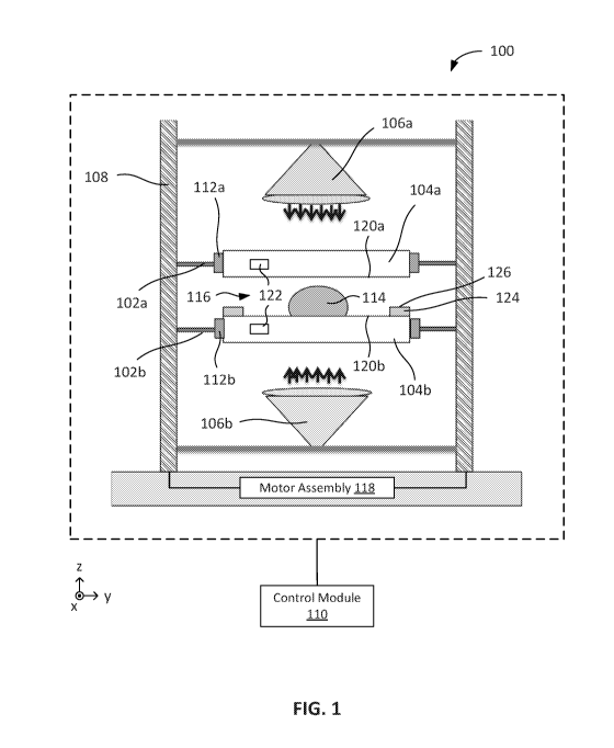
[00123[ An example system 100 for producing polymer film is shown in FIG.
1.
The system 100 includes two actuab]e stages 102a and 102b, two mold structures
104a
and 104b, two light sources 106a and 106b, a support frame 108, and a control
module
110.
[00124[ During operation of the system 100, the two mold structures 104a
and
104b (also referred to as "optical flats") are secured to the actuable stages
102a and
102b, respectively (e.g., through clamps 112a and 112b). In some cases, the
clamps
112a and 112b can be magnetic (e.g., electromagnets) and/or pneumatic clamps
that
enable the mold structures 104a and 104b to be reversibly mounted to and
removed
from the actuable stages 102a and 102b. In some cases, the clamps 112a and
112b can
be controlled by a switch and/or by the control module 110 (e.g., by
selectively applying
14
CA 03076669 2020-03-19
WO 2019/079480
PCT/US2018/056326
electricity to the electromagnets of the clamps 112a and 112b and/or
selectively
actuating pneumatic mechanisms to engage or disengage the molds structures).
[00125[ A photocurable material 114 (e.g., a photopolymer or light-
activated
resin that hardens when exposed to light) is deposited into the mold structure
104b. The
mold structures 104a and 104b are moved into proximity with one another (e.g.,
by
moving the actuable stages 102a and/or 102b vertically along the support frame
108),
such that the photocurable material 114 is enclosed by the mold structures
104a and
104b. The photocurable material 114 is then cured (e.g., by exposing the
photocurable
material 114 to light from the light sources 106a and/or 106b), forming a thin
film
having one or more features defined by the mold structures 104a and 104b.
After the
photocurable material 114 has been cured, the mold structures 104a and 104b
are
moved away from each other (e.g., by moving the actuable stages 102a and/or
102b
vertically along the support frame 108), and the film is extracted.
1001261 The actuable stages 102a and 102b are configured to support the
mold
structures 104a and 104b, respectively. Further, the actuable stages 102a and
102b are
configured to manipulate the mold structures 104a and 104b, respectively, in
one or
more dimensions to control a gap volume 116 between the mold structures 104a
and
104b.
[00127( For instance, in some cases, the actuable stage 102a can
translate the
mold structure 104a along one or more axes. As an example, the actuable stage
102a
can translate the mold structure 104a along an x-axis, a y-axis, and/or a z-
axis in a
Cartesian coordinate system (i.e., a coordinate system having three
orthogonally
arranged axes). In some cases, the actuable stage 102a can rotate or tilt the
mold
structure 104a about one or more axes. As an example, the actuable stage 102a
can
rotate the mold structure 104a along an x-axis (e.g., to "roll" the mold
structure 104a),
a y-axis (e.g., to "pitch" the mold structure 104a), and/or a z-axis (e.g., to
"yaw" the
mold structure 104a) in a Cartesian coordinate system. Translation and/or
rotation with
respect to one or more other axes are also possible, either in addition to or
instead of
those described above. Similarly, the actuable stage 102b can also translate
the mold
structure 104b along one or more axes and/or rotate the mold structure 104b
about one
or more axes.
CA 03076669 2020-03-19
WO 2019/079480
PCT/US2018/056326
[00128[ In some cases, the actuable stages 102a can manipulate the mold
structure 104a according to one or more degrees of freedom (e.g., one, two,
three, four,
or more degrees of freedom). For instance, the actuable stage 102a can
manipulate the
mold structure 104a according to six degrees of freedom (e.g., translation
along an x-
axis, y-axis, and z-axis, and rotation about the x-axis, y-axis, and z-axis).
Manipulation
= according to one or more other degrees of freedom is also possible,
either in addition
to or instead of those described above. Similarly, the actuable stage 102b can
also
manipulate the mold structure 104b according to one or more degrees of freedom
[00129[ In some cases, the actuable stages 102a and 102b can include one
or
more motor assemblies configured to manipulate the mold structures 104a and
104b
and control the gap volume 116. For example, the actuable stages 102a and 102b
can
include a motor assembly 118 configured to manipulate the actuable stages 102a
and
102b, thereby repositioning and/or reorienting the actuable stages 102a and
102b.
1001301 In the example shown in FIG. 1, the actuable 102a and 102b can
both be
moved relative to the support frame 108 to control the gap volume 116. In some
cases,
however, one of the actuable stages can be moved relative to the support frame
108,
while the other can remain static with respect to the support frame 108. For
example,
in some cases, the actuable stage 102a can be configured to translate in one
or more
dimensions relative to the support frame 108 through the motor assembly 118,
while
the actuable stage 102b can be held static with respect to the support frame
108.
[00131[ The mold structures 104a and 104b collectively define an
enclosure for
the photocurable material 114. For example, the mold structures 104a and 104b,
when
aligned together, can define a hollow mold region (e.g., the gap volume 116),
within
which the photocurable material 114 can be deposited and cured into a film.
The mold
structures 104a and 104b can also define one or more structures in the
resulting film.
For example, the mold structures 104a and 104b can include one or more
protruding
structures (e., gratings) from the surfaces 120a and/or 120b that impart a
corresponding
channel in the resulting film. As another example, the mold structures 104a
and 104b
can include one or more channels defined in the surfaces 120a and/or 120b that
impart
a corresponding protruding structure in the resulting film. In some cases, the
mold
structures 104a and 104b can impart a particular pattern on one or both sides
of the
resulting film. In some cases, the mold structures 104a and 104b need not
impart any
16
a CA 03076669 2020-03-19
WO 2019/079480
PCT/US2018/056326
pattern of protrusions and/or channels on the resulting film at all. In some
cases, the
mold structures 104a and 104b can define a particular shape and pattern, such
that the
resulting film is suitable for use as an eyepiece in an optical imaging system
(e.g., such
that the film has one or more light diffractive microstructures or
nanostructures that
impart particular optical characteristics to the film).
[00132[ In some cases, the surfaces of the mold structures 104a and 104b
that
face each other can each be substantially flat, such that the gap volume 116
defined
between them exhibits a 'ITV of 500 nm or less. For example, the mold
structure 104a
can include a substantially flat surface 120a, and the mold structure 104b can
have
substantially flat surface 120b. A substantially flat surface can be, for
example, a
surface that deviates from a flatness of an ideal flat surface (e.g., a
perfectly flat surface)
by 100 nm or less (e.g., 100 nm or less, 75 nm or less, 50 nm or less, etc.).
A
substantially flat surface can also have a local roughness of 2 nm or less
(e.g., 2 nm or
less, 1.5 nm or less, 1 urn or less, etc.) and/or an edge-to edge flatness of
500 nm or less
(e.g., 500 nm or less, 400 nm or less, 300 nm or less, 50 nm or less, etc.).
In some
cases, one or both of the surfaces of the mold structures 104a and 104b can be
polished
(e.g. to further increase the flatness of the surfaces). A substantially flat
surface can be
beneficial, for example, as it enables the mold structures 104a and 104b to
define a gap
volume 116 that is substantially consistent in thickness along the extent of
the mold
structures 104a and 104b (e.g., having a TTV of 500 nm or less). Thus, the
resulting
optical films can be flat (e.g., having a total thickness variation [TTV]
and/or a local
thickness variation [LTV] less than or equal to a particular threshold value,
for example
less than 500 nm, less than 400 nm, less than 300 nm, etc.). Further, polished
mold
structures 104a and 104b can be beneficial, for example, in providing smoother
optical
films for optical imaging applications. As an example, eyepieces constructed
from
smoother optical films may exhibit improved imaging contrast.
[00133( The TTV and LTV of an example optical film 1000 are shown in FIG.
10. The TTV of the optical film 1000 refers to the maximum thickness of the
optical
film 1000 with respect to the entirety of the optical film 1000 (Tmax ), minus
the
minimum thickness of the optical film 1000 with respect to the entirety of the
optical
film 1000 (Tmin) (e.g., TTV = Tma, ¨ Train). The LTV of the optical film 1000
refers
to the maximum thickness of the optical film 1000 with respect to a localized
portion
17
CA 03076669 2020-03-19
WO 2019/079480
PCT/US2018/056326
of the optical film 1000 (Tiocat max), minus the minimum thickness of optical
film 1000
with respect to the localized portion of the optical film 1000 (T/,,,,,/ min)
(e.g., LTV =
Tiocat max ¨ Tlocal min). The size of the localized portion can differ,
depending on the
application. For example, in some cases, the localized portion can be defined
as a
portion of the optical film having a particular surface area. For instance,
for optical
films intended for used as eyepieces in an optical imaging system, the surface
area of
the localized portion can be an area having a 2.5-inch diameter. In some
cases, the
surface area of the localized portion can differ, depending on the eyepiece
design. In
some cases, the surface area of the localized portion can differ, depending on
the
dimensions and/or features of the optical film.
[00134[ The mold structures 104a and 104b are also rigid, such that they
do not
flex or bend during the film production process. The rigidity of the mold
structures
104a and 104b can be expressed in terms of its bending stiffness, which is a
function of
the elastic modulus of the mold structures (E) and the second moment of area
of the
mold structures (I). In some cases, the mold structures each can have a
bending
stiffness of 1.5 Nm2 or greater.
[00135[ Further still, the mold structures 104a and 104b can be partially
or fully
transparent to radiation at one or more wavelengths suitable for photocuring
the
photocurable material (e.g., between 315 nm and 430 nm). Further still, the
mold
structures 104a and 104b can the made from a material that is thermally stable
(e.g.,
does not change in size or shape) up to a particular threshold temperature
(e.g., up to at
least 200 C). For example, the mold structures 104a and 104b can be made of
glass,
silicon, quartz, Teflon, and/or poly-dimethyl-siloxane (PDMS), among other
materials.
[00136[ In some cases, the mold structures 104a and 104b can have a
thickness
greater than a particular threshold value (e.g., thicker than 1 mm, thicker
than 2 mm,
etc.). This can be beneficial, for example, as a sufficiently thick mold
structure is more
difficult to bend. Thus, the resulting film is less likely to exhibit
irregularities in
thickness. In some cases, the thickness of the mold structures 104a and 104b
can be
within a particular range. For example, each of the mold structures 104a and
104b can
be between 1 mm and 50 mm thick. The upper limit of the range could
correspond, for
example, to limitations of an etching tool used to pattern the mold structures
104a and
104b. In practice, other ranges are also possible, depending on the
implementation.
18
CA 03076669 2020-03-19
WO 2019/079480
PCT/US2018/056326
[00137[ Similarly, in some cases, the mold structures 104a and 104b can
have a
diameter greater than a particular threshold value (e.g., greater than 3
inches). This can
be beneficial, for example, as it enables relatively larger films and/or
multiple
individual films to be produced simultaneously. Further, if unintended
particulate
matter is entrapped between the mold structures (e.g., between a spacer
structure 124
and an opposing mold structure 104a or 104b, such as at a position 126), its
effect on
the flatness of the resulting filming film is lessened.
[00138[ For instance, for mold structures 104a and 104b having a
relatively small
diameter, a misalignment on one side of the mold structures 104a and 104b
(e.g., due
to entrapped particulate matter on one of the spacer structures 124, such as
at the
position 126) may result in a relatively sharper change in thickness in the
gap volume
116 along the extent to the mold structures 104a and 104b. Thus, the resulting
film or
films exhibit more sudden changes in thickness (e.g., a steeper slope in
thickness along
the length of the film).
[00139[ However, for mold structures 104a and 104b having a comparatively
larger diameter, a misalignment on one side of the mold structures 104a and
104b will
result in a more gradual change in thickness in the gap volume 116 along the
extent to
the mold structures 104a and 104b. Thus, the resulting film or films exhibit
less sudden
changes in thickness (e.g., a comparatively more gradual slope in thickness
along the
length of the film). Accordingly, mold structures 104a and 104b having a
sufficiently
large diameter are more "forgiving" with respect to entrapped particulate
matter, and
thus can be used to produce more consistent and/or flatter films.
[00140[ As an example, if a particle of 5 gm or less is entrapped along a
point at
the periphery of the mold structures 104a and 104b (e.g., at the position
126), and the
mold structures 104a and 104b each have a diameter of 8 inches, a gap volume
having
a horizontal surface area of 2 square inches within the extent of the mold
structures
104a and 104b will still have a TTV of 500 nm or less. Thus, if a photocurable
material
is deposited within the gap volume, the resulting film will similarly exhibit
a TTV of
500 nm or less.
[00141[ The light sources 106a and 106b are configured to generate
radiation at
one or more wavelengths suitable for photocuring the photocurable material
114. The
one or more wavelengths can differ, depending on the type of photocurable
material
19
CA 03076669 2020-03-19
WO 2019/079480
PCT/US2018/056326
used. For example, in some cases, a photocurable material (e.g., an
ultraviolet light-
curable liquid silicone elastomer such as Poly(methyl methacrylate) or
Poly(dimethylsiloxane)) can be used, and correspondingly the light source can
be
configured to generate radiation having a wavelength in a range from 315 nm to
430
nm to photocure the photocurable material. In some cases, one or more of the
mold
structures 104a and 104b can be transparent, or substantially transparent to
radiation at
the suitable for photocuring the photocurable material 114, such that
radiation from the
light sources 106a and/or 106b can pass through the mold structures 104a
and/or 104b
and impinge upon the photocurable material 114.
[00142[ The control module 110 is communicatively coupled to the actuable
stages 102a and 102b, and is configured to control the gap volume 116. For
instance,
the control module 110 can receive measurements regarding gap volume 116
(e.g., the
distance between the mold structures 104a and 104b at one or more locations)
from the
sensor assembly 122 (e.g., a device having one or more capacitive and/or
pressure-
sensitive sensor elements) and reposition and/or reorient one or both of the
mold
structures 104a and 104b in response (e.g., by transmitting commands to the
actuable
stages 102a and 102b).
[00143[ As described herein, to improve the quality and consistency of the
film,
the position of the two molds can be precisely controlled, such that the molds
are kept
parallel to each other immediately prior to and/or during the curing of the
material. In
some cases, this can be achieved, at least in part, through the use of
physical registration
features positioned on one or more of the molds.
[00144[ As an example as shown in FIG. 1, the system 100 can include one
or
more spacer structures 124 (e.g., protrusions or gaskets) that project from
one or more
surfaces of the mold structure (e.g., mold structure 104b) and towards an
opposing mold
structure (e.g., mold structure 104a). The spacer structures 124 can each have
a
substantially equal vertical height, such that when the mold structures 104a
and 104b
are brought together (e.g., pressed together), the spacer structures 124 abut
the mold
structures 104a and 104b and a substantially flat gap volume 116 is defined
between
them.
[00145[ Further, spacer structures 124 can be positioned in proximity to
and at
least partially enclosing the area of the mold structures 104a and 104b for
receiving and
CA 03076669 2020-03-19
WO 2019/079480
PCT/US2018/056326
curing the photocurable material 114. This can be beneficial, for example, as
it enables
the system 100 to produce polymer films having a low TTV and/or LTV, without
necessarily requiring that a low TTV and/or LTV be maintained across the
entirety of
the extend of the mold structures 104a and 104b. For example, multiple
different
polymer films can be produced without the need of achieving low Try over the
entire
volume between the mold structures 104a and 104b. Accordingly, the throughput
of
the production process can be increased.
[00146[ For example, FIG. 2 shows an example mold structures 104a and 104b
with spacer structures 124 disposed between them. When the mold structures
104a and
104b are brought together, the spacer structures 124 abut the mold structures
104a and
104b and physically obstruct the mold structures 104a and 104b from getting
any nearer
to each other than the vertical height 202 of the spacer structures 124. As
the vertical
height 202 of each of the spacer structures 124 is substantially equal, a
substantially flat
gap volume 116 is defined between the mold structures 104a and 104b. In some
cases,
the vertical height 202 of the spacer structures 124 can be substantially
equal to the
desired thickness of the resulting film.
[00147[ The spacer structures 124 can be constructed from various
materials. In
some cases, the spacer structures 124 can be constructed from a material that
is
thermally stable (e.g., does not change in size or shape) up to a particular
threshold
temperature (e.g., up to at least 200 C). For example, the spacer structures
124 can be
made of glass, silicon, quartz, and/or Teflon, among other materials. In some
cases, the
spacer structures 124 can be constructed from the same material as the mold
structures
104a and/or 104b. In some cases, the spacer structures 124 can be constructed
from a
different material as the mold structures 104a and/or 104b. In some cases, one
or more
of the spacer structures 124 can be integrally formed with the mold structures
104a
and/or 104b (e.g., etched from the mold structures 104a and/or 104b, imprinted
onto
the mold structures 104a and/or 104b through a lithographic manufacturing
processes,
or additively formed onto the mold structures 104a and/or 104b such as through
an
additive manufacturing processes). In some cases, one or more of the spacer
structures
124 can be discrete from the mold structures 104a and/or 104b, and can be
secured or
affixed to the mold structures 104a and/or 104b (e.g., using glue or other
adhesive).
21
CA 03076669 2020-03-19
WO 2019/079480
PCT/US2018/056326
[00148[ Although two spacer structures 124 are shown in FIG. 2, this is
merely
an illustrative example. In practice, there can be any number of spacer
structures 124
(e.g., one, two, three, four, or more) protruding from the mold structure
104a, the mold
structure 104b, or both. Further still, although FIG. 2 shows the spacer
structures 124
positioned along a periphery of the mold structures 104a and 104b, in
practice, each
spacer structures 124 can be positioned anywhere along the extent of the mold
structures 104a and 104b.
[00149[ For instance, FIG. 3A shows an example mold structure 104b having
multiple spacer structures 124 positioned along a periphery of the surface
120b.
Further, the spacer structures 124 surround an area 302 of the surface 120b
for receiving
the photocurable material 114. Accordingly, when a portion of photocurable
material
114 is deposited along the area 302 and the mold structure 104b is brought
together
with another mold structure 104a, the spacer structures 124 abut the mold
structures
104a and 104b and physically obstruct the mold structures 104a and 104b from
getting
any nearer to each other than the vertical height of the spacer structures
124. Thus,
when the photocurable material 114 is cured, the resulting film will have a
constant
height defmed by the vertical height of the spacer structures 124.
[00150[ FIG. 3B shows another example mold structure 104b having multiple
spacer structures 124. In this example, the spacer structures 124 are
positioned along a
periphery of the surface 120b, as well as dispersed along an interior of the
surface 120b.
Further, the spacer structures 124 surround multiple different areas 304 of
the surface
120b for receiving the photocurable material 114. Accordingly, when portions
of
photocurable material 114 is deposited along each of the areas 304 and the
mold
structure 104b is brought together with another mold structure 104a, the
spacer
structures 124 abut the mold structures 104a and 104b and physically obstruct
the mold
structures 104a and 104b from getting any nearer to each other than the
vertical height
of the spacer structures 124. Thus, when the photocurable material 114 is
cured, the
resulting films will each have a constant height defined by the vertical
height of the
spacer structures 124.
[00151[ In some cases, spacer structures can defme a continuous perimeter
around an area of the mold structure for receiving photocurable material
(e.g., a
continuous gasket that surrounds the area). In some cases, spacer structures
can define
22
= CA 03076669 2020-03-19
WO 2019/079480
PCT/US2018/056326
a discontinuous perimeter around an area of the mold structure for receiving
photocurable material (e.g., an alternating sequence of protrusions and gaps
that that
surround the area). In some cases, spacer structures can define one or more
continuous
perimeters and/or one or more discontinuous perimeters around an area.
[00152( As an example, FIG. 4A shows an overhead view of an example mold
structure 104b. The mold structure 104b has multiple sets of spacer structures
124a-d.
In this example, a first set of spacer structures 124a are positioned along a
periphery of
the surface 120b. Further, a second set of spacer structures defines a
continuous
perimeter (e.g., a rectangular perimeter) around a first area 402a for
receiving
photocurable material 114. Further, a third set of spacer structures 124c
defines a
discontinuous perimeter (e.g., a circular perimeter) around a second area 402b
for
receiving photocurable material 114. Further, a fourth set of spacer
structures 124d
defines another discontinuous perimeter (e.g., a polygonal perimeter) around a
third
area 402c for receiving photocurable material 114. In this matter, multiple
different
spacer structures can be positioned along different areas for receiving
photocurable
materials, such that the resulting films from each of those areas will each
have a
constant height. Although example perimeter shapes are shown in FIG. 4A, these
are
merely illustrative examples. In practice, sets of spacer structures can
define perimeters
having any shape, such as circular shapes, elliptical shapes, rectangular
shapes,
polygonal shapes, or any other shape.
[00153[ In some cases, spacer structures can define a perimeter along an
edge
the mold structure. As an example, FIG. 4B shows an overhead view of another
example mold structure 104b. The mold structure 104b shown in FIG. 4B is
similar in
some respects to that shown in FIG. 4A. For example, in FIG. 4B, the mold
structure
104b has a first set of spacer structures 124a positioned along a periphery of
the surface
120b, a second set of spacer structures defining a continuous perimeter (e.g.,
a
rectangular perimeter) around a first area 402a for receiving photocurable
material 114,
a third set of spacer structures 124c defining a discontinuous perimeter
(e.g., a circular
perimeter) around a second area 402b for receiving photocurable material 114,
and a
fourth set of spacer structures 124d defining another discontinuous perimeter
(e.g., a
polygonal perimeter) around a third area 402c for receiving photocurable
material 114.
In this example, however, the mold structure 104b further includes a fifth set
of spacer
23
=
CA 03076669 2020-03-19
=
=
WO 2019/079480
PCT/US2018/056326
structures 124e defining a discontinuous perimeter (e.g., a circular perimeter
defined
by four arc-like portions) along an edge 400 of the mold structure 104b. The
perimeter
defined by the spacer structures 124e encloses each of the other spacer
structures of the
mold structure 104b (e.g., the spacer structures 124a-d). This set of
enclosing spacer
structures 124e can be useful, for example, in further controlling the
position of the two
molds relative to one another. Thus, the quality and consistency of the
resulting film
can be further improved.
[00154( As shown in FIG. 4B, a set of enclosing spacer structures (e.g.,
the set
of spacer structures 124e) can define a discontinuous perimeter. However, this
need
not be the case. For example, in some cases, a set of enclosing spacer
structures can
define a continuous perimeter around the other spacer structures of a mold
structure.
Further as shown in FIG. 4B, a set of enclosing spacer structures can define a
circular
perimeter. However, this also need not be the case. For example, in some
cases, a set
of enclosing spacer structure can define other shapes (e.g., a circular shape
an elliptical
shape, a rectangular shape, a polygonal shape, or any other shape). Further
still, in
some cases, the shape of the perimeter defined by the set of enclosing spacer
structures
can be similar to or identical to the shape defined by the edge 400. For
example, as
shown in FIG. 4B, both can be circular in shape. In some cases, the shape of
the
perimeter defined by the set of enclosing spacer structures can be different
than the
shape defined by the edge 400. For example, one can be circular in shape, and
the other
can be polygonal in shape.
E001551 As described herein, in some cases, mold structures can include
one or
more recesses (e.g., grooves) defined along one or more surfaces of the mold
structure
that accept one or more spacer structures from an opposing mold structure. The
spacer
structures and/or recesses can be used to physically align the molds, such
that the
relative orientation of the mold surfaces are less likely to deviate from the
intended
orientation. For example, the spacer structures and/or recesses can be used to
maintain
a parallel orientation between two molds. As a result, the photocurable
material has a
more even thickness, and is less likely to become distorted.
[00156[ As an example, FIG. 5A shows example mold structures 104a and
104b.
The mold structure 104b includes spacer structures 502a and 502b positioned
along a
periphery of the surface 120b. In this example the spacer structure 502a has a
24
CA 03076669 2020-03-19
WO 2019/079480
PCT/US2018/056326
corresponding recess 504a defined on the surface 120a of the opposing mold
structure
104a, while the spacer structures 504b does not. When portions of photocurable
material 114 are deposited along an area 506 and the mold structures 104a and
104b
are brought together, the spacer structures 502a and 504a abut the mold
structures 104a
and 104b and physically obstruct the mold structures 104a and 104b from
getting any
nearer to each other than either the vertical height of the spacer structure
502b, or the
vertical height of the spacer structure 502a minus a vertical depth of the
recess structure
504a.
[00157[ For example, the spacer structure 502a slots or inserts into the
recess
504a, which prevents the mold structures 104a and 104b from getting any nearer
of
each other. Further, due to the walls of the recess 504a, the spacer structure
502a is
horizontally secured within the recess 504a. Accordingly, the mold structure
104a and
104b cannot horizontally move with respect to another. As another example, the
spacer
structure 502b does not have a corresponding recess, and instead directly
abuts the
surface 120a of the mold structure 104a. Thus, although the spacer structure
502b also
prevents the mold structures 104a and 104b from getting any nearer to each
other, the
spacer structure 502b does not horizontally secure the mold structures 104a
and 104b
relative to one another.
[00158[ Further, as shown in FIG. 5A, the mold structures 104a and 104b
also
define a pattern of gratings 508 along the area 506. Thus, when the
photocurable
material 114 is cured, the resulting film will have a particular pattern of
gratings defined
along its length.
[00159[ Although example spacer structure and recess shapes as shown in
FIG.
5A, these are merely illustrative examples. In practice, the shape of each
spacer
structure and/or recess can vary, depending on the implementation. As an
example,
FIG. 5B shows another example mold structure 104a and another example mold
structure 104b. In this example, the mold structure 104b includes spacer
structures
502c and 502d positioned along a periphery of the surface 120b, each having a
corresponding recess 504b and 504c, respectively, defined on the surface 120a
of the
opposing mold structure 104a.
[00160[ The spacer structure 502c and the recess 504b have corresponding
triangular cross-sections. Accordingly, when the mold structures 104a and 104b
are
CA 03076669 2020-03-19
=
s
WO 2019/079480
PCT/US2018/056326
brought together, the spacer structure 502c slots or inserts into the recess
504b, which
prevents the mold structures 104a and 104b from getting any nearer of each
other than
a distance d. Further, due to the walls of the recess 504b, the spacer
structure 502b is
horizontally secured within the recess 504b. Accordingly, the mold structure
104a and
104b cannot horizontally move with respect to another example.
[00161[ However, the spacer structures and recesses need not have
identical
cross-sectional shapes. For example, as shown in FIG. 5B, the spacer structure
502d
has a triangular cross-section, and the recess 504c has rectangular cross-
section.
Although the spacer structure 502d and the recess 504c are different cross-
sectional
shapes, the recess 504c is configured to receive at least a portion of the
spacer structure
502d. Accordingly, when the mold structures 104a and 104b are brought
together, the
spacer structure 502d slots or inserts partially into the recess 504c, which
prevents the
mold structures 104a and 104b from getting any nearer of each other than a
distance d.
Further, due to the walls of the recess 504c, the spacer structure 502d is
similarly
horizontally secured within the recess 504c. Accordingly, the mold structure
104a and
104b cannot horizontally move with respect to another example.
[00162[ Similarly, as shown in FIG. 5B, the mold structures 104a and 104b
also
define a pattern of gratings 510 along an area 512. Thus, when the
photocurable
material 114 is deposited into the area 512 and cured, the resulting film will
have a
particular pattern of gratings defined along its length.
[00163[ The dimensions of each of these features can vary, depending on
the
implementation. In some implementations, the width of a spacer structure can
be
between 0.01 cm to 1 cm. In some implementations, the height of a spacer
structure
can be between 100 pm and 900 pm. The geometry of the spacer structures can be
rectangular prism, cylinder, and other three-dimensional shapes (e.g., a
complex three-
dimensional shape).
[00164[ Further, each spacer structure and/or recess can be substantially
flat. For
instance, each spacer structure and/or recess can have a total thickness
variation of 100
nm or less, such that when a spacer structure and recess are brought together,
the
distance between their respective mold structures deviate from an expected or
designed
distance by 100 nm or less. As an example, for a spacer structure and a recess
each
having a respective rectangular cross section, the surfaces of the spacer
structure and
26
CA 03076669 2020-03-19
WO 2019/079480
PCT/US2018/056326
the recesses can be sufficiently flat and accurately formed, such that when
they are
brought together, the distance between their corresponding mold structures
deviate
from an expected or designed distance by 100 nm or less. As another example,
for a
spacer structure having a triangular cross section and a recess having a
rectangular cross
section (e.g., as shown in FIG. 5B), the slopes of the triangular spacer
structure and the
surfaces of the recess can be sufficiently flat and accurately formed, such
that when the
spacer structure and recess are brought together, the distance between their
corresponding mold structures deviate from an expected or designed distance by
100
nm or less.
[00165[ Further, although different spacer structures and recesses are
shown in
FIGS. 5A and 5B, there are merely illustrative examples. In practice, spacer
structures
and/or recess having different physical configurations also can be used,
either instead
or in addition to those shown. As an example, as shown in FIG. 5C, a spacer
structure
502e can have a portion 514 with a rectangular cross-section, and a distal end
516
having a substantially hemispherical shape. As another example, as shown in
FIG. 5C,
a spacer structure 502f can have a portion 518 with a rectangular cross-
section, and a
number of rounded corners 520 at its distal end 522. As another example, as
shown in
FIG. 5C, a spacer structure 502g can have a portion 524 with a trapezoidal
cross-section
(e.g., a triangle shape with a corner removed), and a rounded distal end 526.
As another
example, a spacer structure can have a substantially polygonal cross-section
(e.g.,
triangular, quadrilateral, pentagonal, hexagonal, etc.) with one or more
rounded corners
instead of sharp corners.
[00166[ Similarly, recesses can also include one or more rounded features.
As
an example, as shown in FIG. 5D, a recess 504e can have a portion 528 with a
rectangular cross-section, and an interior end 530 having a substantially
hemispherical
shape. As another example, as shown in FIG. 5D, a recess 504f can have a
portion 532
with a rectangular cross-section, and a number of rounded corners 534 at its
interior
end 536. As another example, as shown in FIG. 5D, a recess 504g can have a
portion
538 with a trapezoidal cross-section (e.g., a triangle shape with a corner
removed), and
a rounded interior end 540. As another example, a recess can have a
substantially
polygonal cross-section (e.g., triangular, quadrilateral, pentagonal,
hexagonal, etc.)
with one or more rounded comers instead of sharp corners.
27
CA 03076669 2020-03-19
WO 2019/079480
PCT/US2018/056326
[00167[ These configurations can be useful, for example, as they reduce or
eliminate the presence of sharp edges or corners in the regions in which the
spacer
structures interface with their corresponding recesses. Thus, this can reduce
wear and
tear on the spacer structures and/or the recesses. Further, this can enable
the mold
structures to better maintain their flatness over repeated usages (e.g., by
reducing point
contacts between them).
[00168[ In some cases, the system 100 (via the arrangement of the spacer
structures and corresponding recesses on the mold structures) can position the
mold
structures such that the thickness of the gap volume 116 (e.g., the distance
between the
mold structures) is between 20 pm and 2 mm. In some cases, the photocurable
material
114 can be deposited into at least one of the mold structures 104a and 104b
prior to the
system 100 positioning the mold structures 104a and 104b against each other at
this
distance. This can be beneficial, for example, as it may be easier or more
convenient
to introduce photocurable material 114 while the mold structures are further
apart,
rather than when they are positioned close together. Nevertheless, in some
cases,
photocurable material 114 can be deposited into the mold structures after they
have
been brought together (e.g., through an injection tube or needle positioned
through one
or more of the mold structures).
[00169[ In the examples shown in FIGS. 5A and 5B, some of the spacer
structures (e.g., spacer structures 502a, 502c, and 502d) are configured to
slot or insert,
at least partially, into a corresponding recess (e.g., recesses 504a, 504b,
and 504c,
respectively), such that the spacer structures are horizontally secured within
the
recesses. In this configuration, the spacer structure is "locked" within a
corresponding
recess, and cannot move relative to the recess along any horizontal direction.
[00170[ However, in some cases, spacer structures and recesses can be
configured such that in a slotted configuration, the spacer structure retains
one or more
horizontal degrees of freedom relative to the recess. For example, in some
cases, a
spacer structure and a recess can be configured such that when the spacer
structure is
slotted into the recess, the recess prevents the spacer structure from moving
with respect
to the recess along one or more first horizontal directions, but allows the
spacer
structure to move with respect to the recess along one or more second
horizontal
directions.
28
CA 03076669 2020-03-19
WO 2019/079480
PCT/US2018/056326
[001711 As an example, FIG. 6A shows an overhead view of another example
mold structure 104a (indicated in outline) overlaid atop another example mold
structure
104b (indicated using shaded shapes). The mold structure 104b includes spacer
structures 602a-c positioned around an area 606 between the mold structures
104a and
104b. Further, each of the spacer structures 602a-c has a corresponding recess
604a-c
defined along the surface of the mold structure 104a. When portions of
photocurable
material 114 is deposited along the area 606 and the mold structures 104a and
104b are
brought together, the spacer structures 602a-c slot into the recesses 604a-c
and
physically obstruct the mold structures 104a and 104b from getting any nearer
to each
other.
[00172( Further, each recess 604a-c has a cross-section area that is
larger than its
corresponding spacer structure 602a-c, and defines a slot or path along which
the spacer
structure 602a-c can horizontally translate within it. For example, the recess
604a
defines a slot or path that enables the spacer structure 602a to slide within
it along a
direction 608a. A cross-sectional view of the interaction between the recess
604a and
the spacer structure 602a is shown in FIG. 6B. Further, the recess 604b
defines a slot
or path that enables the spacer structure 602b to slide within it along a
direction 608b.
Further still, the recess 604c defines a slot or path that enables the spacer
structure 602c
to slide within it along a direction 608c. However, as the directions 608a-c
are not
parallel to each other, when all of the spacer structures 602a-c are slotted
within their
corresponding recesses 604a-c, the mold structures 102a and 102b are
horizontally
locked to one another. Thus, multiple different sets of spacer structures and
recesses
can be used to register the position of one mold structure relative to another
in a "self-
locking" manner.
[00173[ Nevertheless, in some cases, a spacer structure and a recess can
be
configured such that when the spacer structure is slotted into the recess, the
spacer
structure is locked within a corresponding recess, and cannot move relative to
the recess
along any horizontal direction.
[00174[ As an example, FIG. 7A shows an overhead view of another example
mold structure 104a (indicated in outline) overlaid atop another example mold
structure
104b (indicated using shaded shapes). The mold structure 104b includes spacer
structures 702a and 702b positioned around an area 706 between the mold
structures
29
CA 03076669 2020-03-19
WO 2019/079480
PCT/US2018/056326
104a and 104b. Further, each of the spacer structures 702a and 702b has a
corresponding recess 704a and 704b defined along the surface of the mold
structure
104a. When portions of photocurable material 114 is deposited along the area
706 and
the mold structures 104a and 104b are brought together, the spacer structures
702a and
702b slot into the recesses 704a and 704b and physically obstruct the mold
structures
104a and 104b from getting any nearer to each other. Further, each recess 704a
and
704b has a cross-sectional area and a shape similar to those of its
corresponding spacer
structure 702a and 704b. A cross-sectional view of the interaction between the
recess
704a and the spacer structure 702a is shown in FIG. 7B. Thus, when each spacer
structure 702a and 702b is slotted into its corresponding recess 704a and
704b, it is
snuggly retained within the recess and cannot move relative to the recess
along any
horizontal direction.
1001751 As described herein, although various example spacer structures
and
recesses are shown and described, it is understood that any combination of
spacer
structures and recesses can be used in any particular embodiment. As an
example, FIG,
8 shows an overhead view of another example mold structure 104a (indicated in
outline)
overlaid atop another example mold structure 104b (indicated using shaded
shapes).
The mold structure 104a includes several different spacer structures 802a-h
positioned
around an area 806 between the mold structures 104a and 104b. Further, each of
the
spacer structures 802a-h has a different corresponding recess 804a-h defined
along the
surface of the mold structure 104b. As shown in FIG. 8, some of the sets of
spacer
structures and recesses allow for relative horizontal movement with respect to
one or
more directions (e.g., spacer structure 802d and recess 804d, and spacer
structure 802f
and recess 8040. Further, some of the sets of spacer structures and recesses
do not
allow for relative horizontal movement (e.g., the remaining sets of spacer
structures and
recesses shown in FIG. 8). In practice, other combinations are also possible,
depending
on the implementation.
[001761 Further, although of the examples shown herein include spacer
structures protruding from a common mold structure, this need not be the case.
In
practice, there can be any number of spacer structures (e.g., one, two, three,
four, or
more) protruding either from a single mold structure or from both mold
structures.
Further, although of the examples shown herein include recesses defined along
a
CA 03076669 2020-03-19
WO 2019/079480
PCT/US2018/056326
common mold structure, this also need not be the case. In practice, there can
be any
number of recesses (e.g., one, two, three, four, or more) defined either along
a single
mold structure or along both mold structures.
[00177[ In some cases, spacer structures and/or recesses can be formed
through
lithographical techniques. For example, spacer structures and/or recesses can
be
patterned through lithography, and etched using thy etch techniques such as
reactive
ion etch (RIE), inductively coupled plasma (ICP) and/or sputter etch
techniques. In
some cases, spacer structures and/or recesses can be etched in glass, silicon,
and/or
metal substrates.
[00178[ Further, in some cases, spacer structures and/or recesses (e.g.,
those
having angled surfaces) can be implemented in glass, fused silica, silicon,
metals, or
other materials using gray-scale lithography. For example, gray-scale
lithography can
be used to pattern a three-dimension resist layer as a mask, and transfer the
geometries
into a substrate by dry etch techniques such as ME, ICP, and/or sputter etch.
For silicon
substrates, the angled sidewall surfaces can also be fabricated using wet
chemical
etching (e.g., to define linear top-view shapes, such as on the on x-y plane,
depending
on the crystalline orientation of the silicon wafer used). For example, in
(100) silicon
wafer, the top-view shapes/geometries of the spacer structures and/or recesses
will align
to the <110> direction, and the sidewall will have 54.70 angle from the
horizon. The
top-view shapes/geometries can be patterned through lithography, and etched in
the z
direction using dry etch techniques (e.g., for hard mask) and then using wet
etch
techniques (e.g., for silicon, such as KOH and TMAH).
[00179( In some cases, spacer structures can be formed through additive
manufacturing techniques (e.g., 3D printing and two-photon laser printing). In
some
cases, the printed polymer structures can be directly used as spacer
structures. In some
case, she printer polymer structures can be used as three-dimension mask
layer, and
transfer the geometries into a substrate by dry etch techniques such as ME,
ICP, and/or
sputter etch.
[00180( In some cases, a system 100 can also include one or more heating
elements to apply heat to a photocurable material during the curing process.
This can
be beneficial, for example, in facilitating the curing process. For instance,
in some
cases, both heat and light can be used to cure the photocurable material. For
example,
31
CA 03076669 2020-03-19
=
A
A
WO 2019/079480
PCT/US2018/056326
the application of heat can be used to accelerate the curing process, make the
curing
process more efficient, and/or make the curing processes more consistent. In
some
cases, the curing process can be performed using heat instead of light. For
example,
the application of heat can be used to cure the photocurable material, and a
light source
need not be used.
[00181( An example system 900 for producing polymer film is shown in
FIG. 9.
In general, the system 900 can be similar to the system 100 shown in FIG. I.
For
example, the system 900 can include two actuable stages 102a and 102b, two
mold
structures 104a and 104b, a support frame 108, and a control module 110. For
ease of
illustration, the control module 110 is not shown in FIG. 9.
[00182[ However, in this example, the system 900 does not include the
two light
sources 106a and 106b. Instead, it includes two heating elements 902a and
902b,
positioned adjacent to the mold structures 104a and 104b, respectively. The
heating
elements 902a and 902b are configured to move with the mold structures 104a
and 104b
(e.g., through the actuable stages 102a and 102b), and are configured to apply
heat to
the photocurable material 114 between the mold structures 104a and 104b during
the
curing process.
[00183[ The operation of the heating elements 902a and 902b can be
controlled
by the control module 110. For example, the control module 110 can be
communicatively coupled to the heating elements 902 and 902b, and can
selectively
apply heat to the photocurable material 114 (e.g., by transmitting commands to
the
heating elements 902a and 902b).
[00184( Example heating elements 902a and 902b metal heating elements
(e.g.,
nichrome or resistance wire), ceramic heating elements (e.g., molybdenum
disilicide or
PTC ceramic elements), polymer PTC heating elements, composite heating
elements,
or a combination thereof. In some cases, the heating elements 902a and 902b
can
include a metal plate to facilitate a uniform transfer heat to the mold
structures 104a
and 104b.
[00185[ Although two heating elements 902a and 902b are shown in FIG.
9, in
some cases, a system can include any number of heating elements (e.g., one,
two, three,
four, or more), or none at all. Further, although the system 900 is shown
without light
32
= CA 03076669 2020-03-19
WO 2019/079480
PCT/US2018/056326
sources 106a and 106b, in some cases, a system can include one or more light
sources
and one or more heating elements in conjunction.
[00186[ FIG. 11 shows an example process 1100 for producing a polymer
product. The process 1100 can be performed, for example, using the systems 100
or
900. In some cases, the process 1100 can be used to produce polymer films
suitable
for use in optical applications (e.g., as apart of eyepieces in an optical
imaging system).
[00187[ In the process 1100, mold structures are mounted to actuable
stages (step
1102). For example, as shown in FIGS. 1 and 9, molds structures 104a and 104b
can
be mounted to actuable stages 102a and 102b, respectively. The mold structures
can
be mounted using clamps (e.g., clamps 112a and 112b) or other attachment
mechanisms. In some cases, the mold structures can be mounted using
electromagnetic
or pneumatic clamps that are selectively controlled by a switch and/or a
control module.
[001881 One or more spacer structures are introduced between the mold
structures (step 1104). As described herein, spacer structures can be disposed
at various
positions between the mold structures (e.g., as shown and described with
respect to
FIGS. 1-9). In some cases, a spacer structure can be integrally formed with a
mold
structure (e.g., etched from the mold structures, imprinted onto the mold
structures
through a lithographic manufacturing processes, or additively formed onto the
mold
structures such as through addition manufacturing processes). In some cases, a
spacer
structure can be separate and distinct from the mold structure, and can be
individually
positioned between the molds structures.
[00189( A photocurable material is dispensed between the mold structures
(step
1106). Example photocurable materials are described herein (e.g., with respect
to FIG.
1). In some cases, photocurable materials can be dispensed along one or more
specific
positions in a gap volume between the mold positions, such that they are at
least
partially enclosed by the spacer structures (e.g., as shown and described with
respect to
FIGS. 3A and 3B).
[001901 In some cases, the photocurable material can be dispensed
differently,
depending on the material. For example, for photocurable materials that shrink
a
relatively small amount (e.g., less than 10%) during the polymerization
process and
exhibit mechanical properties that are not dependent on the casting surface
area, the
photocurable material can be carried out all at once to cover a large area on
the mold
33
CA 03076669 2020-03-19
WO 2019/079480
PCT/US2018/056326
structure, while avoiding contact between the photocurable material and the
spacer
structures (e.g., as shown in FIG. 3A),
1001911 As another example, for photocurable materials that shrink a
relatively
larger amount (e.g., greater than 10%) and exhibit mechanical properties that
are
dependent on the casting surface area, photocurable materials can be dispensed
on the
bottom mold in metered quantities at multiple different locations, such that
individual
dispensed "puddles" of the material do not touch each other or the spacer
structures
(e.g., as shown in FIG. 3B). This can be beneficial, for example, as it
reduces the
surface area of each individual the casted polymer material, such that each is
small
enough to shrink freely and cure more efficiently. This can result in a lower
TT V and/or
LTV, and can enable higher manufacturing throughput.
1001921 In some cases, the photocurable materials can be "pre-polymerized"
prior to dispensing between the mold structures (e.g., such that they are
shrunk, but still
are sufficiently fluid to be effectively dispensed between the mold
structures). A pre-
polymerization process can be performed, for example, by curing the
photocurable
materials (e.g., using UV light and/or heat) at an energy level that makes the
materials
viscous yet still able to flow.
[00193[ The mold structures are positioned in proximity to each other
(step
1108). For example, as described with respect to FIGS. 1 and 9, the actuable
stages
102a and/or 102b can move the mold structures 104a and/or 104b towards each
other,
such that the photocurable material 114 is enclosed between them without a gap
volume. In some cases, the mold structures 104a and 104b can be positioned
such that
a mold structure contacts a spacer structure positioned on the opposing mold
structure
with a particular amount of positive force (e.g., 10 N to 200 N), and locked
into place.
[001941 The photocurable material is cured (step 1110). In some cases, the
photocurable material can be cured using light (e.g., as shown and described
with
respect to FIG. 1). For example, the top and/or the bottom of the photocurable
material
can be irradiated with light (e.g., ultraviolet light). In some cases,
irradiating both sides
of the photocurable material can enable more uniform and faster curing. In
some cases,
the light intensity can be kept uniform across the area of the photocurable
material to
reduce non-uniform shrinkage and its potentially adverse consequences on the
Try
and/or the LTV of resulting polymer products. In some cases, a diffuser can be
34
, CA 03076669 2020-03-19
WO 2019/0'79480
PCT/US2018/056326
positioned between a light source and the photocurable material to improve the
uniformity of light.
[00195[ In some cases, the photocurable material can be cured using heat
(e.g.,
as shown and described with respect to FIG. 9). In some cases, heat can be
applied
along the top and/or the bottom of the photocurable material. In some cases,
heating
both sides of the photocurable material can enable more uniform and faster
curing. In
some cases, metal plates can be positioned between a heating element and a
molds
structure to facilitate a uniform distribution of heat across the mold
structure and the
photocurable material.
[00196[ Further, in some cases, the photocurable material can be cured
using
both light and heat. As an example, thermal curing can be initiated by
exposure to
infrared light. For instance, a photocurable material can be chosen on the
basis that it
absorbs relatively little infrared radiation. Further, the thermal heating of
the
photocurable material can be localized in the photocurable material itself.
This
arrangement can be beneficial, for example, in enabling lower molding cycle
times as
there is less heat to be removed from the mold structure after each curing
processes is
performed. Further, if the photocurable material requires both thermal and
light energy
to cure quickly with optimum properties, both sources could be applied from
either side
or both sides of the mold structures.
[00197[ After the photocurable material is cured, the resulting product is
removed from between the mold structures (step 1112). For example, the mold
structures can be positioned further from each other (e.g., using the actuable
stages),
and the product can be extracted from between them. In some cases, the
extracted
product can have a particular shape suitable for use in a particular
application (e.g., as
defined by the mold structures) without requiring a separate singulation
process (e.g.,
separately cutting out a portion of the cured polymer product according to the
desired
shape). As described herein, in some cases, the product can be a polymer film
suitable
for use in optical applications (e.g., as a part of eyepieces in an optical
imaging system).
In some cases, a small opening in spacer structures can be used to evacuate
excess
photocurable material from between the mold structures.
1001981 As described herein, in some cases, individual polymer products
can be
produced without performing a singulation process. For example, two molds can
be
CA 03076669 2020-03-19
1
=
WO 2019/079480
PCT/US2018/056326
configured such that, when the molds are brought together, they define an
enclosed
region corresponding to the size and shape of single polymer product. During
the
production process, a photocurable material is enclosed between the two molds,
and the
material is cured to form a polymer film. After curing, the polymer film is
extracted
from the molds, resulting in a single polymer product having a particular
predefined
size and shape. This polymer product can be subsequently used in other
manufacturing
processes without the need for an additional singulation step. Accordingly,
the polymer
product is less likely to have physical and/or chemical damage (e.g., compared
to a
polymer product formed through singulation of a larger polymer film), and can
be more
suitable for use in variation-sensitive environments
[00199[ FIG. 12 is a simplified schematic diagram of an example process
for
producing a single polymer product 1200 using the system 100, without
performing a
separate singulation process. The process shown in FIG. 12 can be used, for
example,
to produce optical components, such as waveguides or eyepieces for using a
wearable
imaging headsets. For ease of illustration, portions of the system 100 have
been
omitted.
[00200[ In some cases, the process can be particularly useful for
producing
waveguides or eyepieces suitable for use in a headset. For instance, the
process can be
used to produce waveguides or eyepieces having a thickness and/or cross-
sectional area
that are sufficient to guide light and project light covering a field of view
of a headset
wearer. As an example, the process can be used to produce polymer products
having a
thickness of no more than 1000 gm (e.g., as measured along the z-axis of a
Cartesian
coordinate system), such as 800 gm or less, 600 gm or less, 400 gm or less,
200 gm or
less, 100 gm or less, or 50 gm or less, and an area of at least 1 cm2 (e.g.,
as measured
with respect an x-y plane of the Cartesian coordinate system), such as 5 cm2
or more,
cm2 or more, such as up to about 100 cm2 or less, and having a predetermined
shape.
In certain cases, the polymer film can have a dimension of at least 1 cm
(e.g., 2 cm or
more, 5 cm or more, 8 cm or more, 10 cm or more, such as about 30 cm or less)
in at
least one direction in the x-y plane.
[00201[ As shown in the left portion of FIG. 12, mold structure 104a has a
surface 120a, and the mold structure 104b has a surface 120b facing the
surface 120a
of the mold structure 104a. The mold structures 104a and 104b are configured
such
36
CA 03076669 2020-03-19
= =
WO 2019/079480
PCT/US2018/056326
that, when the molds are brought together, they define an enclosed region
corresponding to the size and shape of single polymer product (e.g., a single
waveguide
or eyepiece). For example, the surface 120a can include a discrete, continuous
first
area 1202a corresponding to the predetermined size and shape of the polymer
product
1200. Similarly, the surface 120b can include a discrete, continuous second
area 1202b
corresponding to the predetermined size and shape of the polymer product 1200.
When
the mold structures 104a and 104b are aligned together, they can define a
hollow mold
region (e.g., a gap volume 116) along the areas 1202a and 1202b corresponding
to the
size and shape of the polymer product 1200, within which the photocurable
material
114 can be deposited and cured into a film. In some cases, the areas 1202 and
1202b
can encompass substantially the entirety of the surfaces 120a and 120b,
respectively.
In some cases, the areas 1202 and 1202b can encompass a portion of the
surfaces 120a
and 120b, respectively.
[002021 As described above, the mold structures 104a and 104b can also
define
one or more structures in the resulting film. For example, the mold structures
104a and
104b can include one or more protruding structures from the surfaces 120a
and/or 120b
of the mold structures that impart a corresponding channel in the resulting
film. As
another example, the mold structures 104a and 104b can include one or more
channels
defined in the surfaces 120a and/or 120b that impart a corresponding
protruding
structure in the resulting film. In some cases, the mold structures 104a and
104b can
define a particular shape and pattern, such that the resulting film is
suitable for use as a
waveguide or eyepiece in an optical imaging system (e.g., such that the film
has one or
more light diffractive microstructures or nanostructures that impart
particular optical
characteristics to the film).
[00203[ As shown in the left portion of FIG. 12, photocurable material 114
is
dispensed onto the mold structures 104a and/or 104b (e.g., dispensed into a
space on or
adjacent of the first area 1202a and/or the second area 1202b). In some cases,
the
photocurable material 114 can be dispensed by a dispensing station or
mechanism, such
as by one or more pumps, pipettes, injectors, syringes, etc. that selectively
dispense a
meter amount of photocurable material). The photocurable material 114 can be
dispensed according to different patterns. As an example, the photocurable
material
114 can be dispensed at multiple different discrete locations along the first
area 1202a
37
CA 03076669 2020-03-19
WO 2019/079480
PCT1US2018/056326
and/or the second area 1202b. As another example, the photocurable material
114 can
be dispensed a single discrete location along the first area 1202a and/or the
second area
1202b. In some cases, the photocurable material 114 can dispensed according to
a
symmetric pattern. In some cases, the photocurable material 114 can be
dispensed
according to an asymmetric pattern. Further, at each discrete location, the
dispensed
photocurable material 114 can have a particular size, volume, and shape.
Example
patterns are shown and described in greater detail with respect to FIGS. 13A-
13E. In
some cases, photocurable material 114 can be dispensed along a single mold
structure
(e.g., the bottom mold structure 104b). In some cases, photocurable material
114 can
be dispensed along both mold structures.
[00204[ As shown in the upper middle portion of FIG. 12, the mold
structures
104a and 104b are moved into proximity with one another (e.g., by moving the
actuable
stages 102a and/or 102b described with respect to FIG. 1), such that the
photocurable
material 114 is enclosed by the mold structures 104a and 104b. The
photocurable
material 114 can be held in place by surface tension of the photocurable
material 114
and/or adhesive forces between the photocurable material 114 and the mold
structures
104a and 104b. Further the confinement of the photocurable material 114
between the
mold structures 104a and 104b can be controlled by dispensing a metered volume
of
the photocurable material 114 (e.g., corresponding to the volume between the
first area
1202a and the second area 1202b). The photocurable material 114 is then cured
(e.g.,
by irradiating the photocurable material 114 with light 1204 suitable for
photocuring
the photocurable material 114), forming a polymer product 1200 having one or
more
features defined by the mold structures 104a and 104b.
1002051 As shown in the right portion of FIG. 12, after the photocurable
material
114 has been cured, the mold structures 104a and 104b are moved away from each
other
(e.g., by moving the actuable stages 102a and/or 102b). The polymer product
1200 is
then extracted (e.g., as shown in the lower middle portion of FIG. 12).
[00206[ As described above, the first area 1202a and second area 1202b
each
correspond to the predetermined size and shape of the polymer product 1200.
Accordingly, the polymer product 1200 is produced without the need to perform
a
separate singulation process. In some cases, after extraction, the polymer
product 1200
38
CA 03076669 2020-03-19
WO 2019/079480
PCT/US2018/056326
can be directly used in other manufacturing processes (e.g., incorporated into
an
apparatus, such as a headset).
[00207[ As described above, photocurable material 114 can be dispensed onto
the mold structures 104a and/or 104b according to different patterns. Several
example
patterns are shown in FIGS. 13A-13E. For ease of illustration, only a single
mold
structure 104b is shown in FIG. 13A-13C. However, it is understood that
photocurable
material 114 can be dispensed into spaces on or adjacent of the mold structure
104a,
the mold structure 104b, or both.
[00208[ As shown in FIG. 13A, photocurable material 114 can be dispensed
according to one or more lines. In practice, the number and arrangement of
lines can
vary. For example, photocurable material 114 can be dispensed according to
one, two,
three, or more lines. Further, each line can extend horizontally, vertically,
or according
to an angle. In some cases, lines can be eventually distributed along a mold
structure
(e.g., spaced evenly from one another). In some cases, lines can be
distributed
according to some other pattern (e.g., spaced unevenly from one another). In
some
cases, each of the lines can have a similar thickness and/or length. In some
cases, one
or more of the lines can differ with respect to thickness and/or length.
Further, lines
need not be straight. For example, one or more lines can be curved or arced.
Further,
in some cases, two or more lines can overlap one another.
[00209( As shown in FIG. 13B, photocurable material 114 also can be
dispensed
according to one or more drops (e.g., substantially ovular or circular
deposits). In
practice, the number and arrangement of dots can vary. For example,
photocurable
material 114 can be dispensed according to one, two, three, or more drops. In
some
cases, dots can be eventually distributed along a mold structure (e.g., spaced
evenly
from one another). In some cases, drops can be distributed according to some
other
pattern (e.g., spaced unevenly from one another). In some cases, each of the
drops can
have a similar size and/or shape. In some cases, one or more of the drops can
differ
with respect to size and/or shape. Further, in some cases, two or more drops
can overlap
one another.
[00210[ As shown in FIG. 13C, photocurable material 114 also can be
dispensed
according to other patterns, such as a free form pattern. In practice, a free
form pattern
can vary. For example, photocurable material 114 can be dispensed at one, two,
three,
39
CA 03076669 2020-03-19
=
=
WO 2019/079480
PCTMS2018/056326
or more discrete locations. Further, the size and shape of each free form
pattern can
vary. Further, in some cases, two or more free form patterns can overlap one
another.
[00211[ Although lines, drops, and free form patterns are shown separately
with
respect to FIGS. 13A-13C, in some cases, photocurable material 114 also can be
dispensed according to one or more of lines, drops, and/or free form patterns
in
combination with respect to a particular mold structure.
[00212[ Further, in some cases, the dispense pattern of the photocurable
material
114 can correspond to one or more localized features along the areas 1202a
and/or
1202b. For example, if areas 1202a and/or 1202b define a feature having a
relatively
larger volume at a particular location (e.g., defining a thicker portion of
the polymer
product), the dispense pattern can include more photocurable material 114 at
that
location. As another example, if areas 1202a and/or 1202b define a feature
having a
relatively smaller volume at a particular location (e.g., defining a thinner
portion of the
polymer product), the dispense pattern can include less photocurable material
114 at
that location.
[00213[ In some cases, the total volume of dispensed photocurable material
114
can be precisely metered or regulated, such that the photocurable material 114
evenly
spreads across the areas 1202a and 1202b, without substantially leaking beyond
the
areas 1202a and/or 1202b. This can be useful, for example, in reducing or
eliminating
material waste. Further, this improves the consistency of the resulting
polymer product
(e.g., the polymer product need not be cut or trimmed to remove excess
photocurable
material that has cured beyond the areas 1202a and/or 1202b). In some cases,
the total
volume of dispensed photocurable material 114 can be substantially equal to
the volume
between the areas 1202 and 1202b when the mold structures 104a and 104b and
aligned.
[00214[ In some cases, photocurable material 114 can be dispensed between
the
mold structures 104a and 104b after the mold structures 104a and 104b have
already
been aligned. As an example, FIG. 13D shows two mold structures 104a and 104b
in
alignment. Photocurable material 114 is dispensed between the mold structures
104a
and 104b by injecting the photocurable material 114 at one or more locations
1302a-e
along the sides of the mold structures 104a and 104b. The injected
photocurable
material 114 spreads between the mold structures 104a and 104b through
capillary
action. In some cases, different amounts of photocurable material 114 can be
injected
CA 03076669 2020-03-19
WO 2019/079480
PCT/US2018/056326
at different locations along the sides of the mold structures 104a and 104b to
facilitate
uniform spreading. Although five locations 1302a-e are shown in FIG. 13D,
these are
merely illustrative examples. In practice, photocurable material 114 can be
injected at
one or more other locations, either instead of or in addition to those shown
in FIG. 13D.
[00215[ In some cases, one or more of the edges between the mold
structures
104a and 104b can be sealed to restrict the flow of injected photocurable
material 114.
For example, FIG. 13E shows two mold structures 104a and 104b in alignment.
The
edges 1304a-e are sealed (e.g., the mold structures 104a and 104b are joined
together
along these edges), while the edge 1304f is open and exposed (e.g., the mold
structures
104a and 104 remain separate along this edge). The photocurable material 114
can be
injected along the edge 1304f to fill the volume between the mold structures
104a and
104b. In this configuration, the mold structures 104a and 104b can be arranged
vertically, such that the exposed edge 1304f is positioned along the top of
the mold
structures 104a and 104b (e.g., to prevent the photocurable material 114 from
pouring
out). The photocurable material 114 can be cured by directing light
horizontally (e.g.,
through the mold structures 104a and/or 104b) instead of vertically (e.g., as
shown in
FIG. 1). Further, in some cases, edges can be reversibly sealed (e.g., using
peelable
glue or tape). Further still, one or more sealed edges can be exposed before
or during
the curing process (e.g., to remove excess materials and/or to release any
stresses
developed during the curing process). Although an example arrangement of
sealed and
exposed edges are shown in FIG. 13E, this is merely an illustrative example.
In
practice, another arrangements of sealed and exposed edges are also possible,
depending on the implementation.
[00216[ As described above, spacer structures can be used to regulate the
spacing
between the mold structures 104a and 104b. Spacer structures can be useful,
for
example, to control the relative orientation of the mold surfaces, such that
the resulting
polymer products are less likely to deviate from their intended shape.
Further, the
resulting polymer products are less likely to become distorted (e.g.,
wrinkled, stretched,
or compressed) during production.
[00217[ In some cases, the spacer structures can be placed beyond the
areas
1202a and 1202b of the mold structures 104a and 104b, such that the
photocurable
material 114 does not come into contact with the spacer structures during the
production
41
CA 03076669 2020-03-19
WO 2019/079480
PCT/US2018/056326
process. This can be beneficial, for example, in improving the quality of
polymer
product (e.g., by reducing unintended variation due to interference between
the spacer
structures and the photocurable material 114).
[00218[ As an example, FIG. 14 shows a mold structure 104b having a
surface
120b. The surface 120b includes a discrete, continuous area 1202b
corresponding to
the predetermined size and shape of a polymer product (e.g., as described with
respect
to FIG. 12). In this example, the mold structure 104b also includes several
protrusions
1402a-d extending beyond the periphery of the area 1202b. Each protrusion
1402a-d
includes a respective spacer structure 1404a-d and a respective fiducial
feature 1406a-
d.
[00219[ The spacer structures 1404a-d can be similar to those described
with
respect to FIGS. 1 and 2. For example, the spacer structures 1404a-d can that
project
from the mold structure 104b and towards an opposing mold structure (e.g., the
mold
structure 104a). Further, the spacer structures 1404a-d can each have a
substantially
equal vertical height, such that when the mold structures 104a and 104b are
brought
together (e.g., pressed together), the spacer structures 1404a-d abut the mold
structures
104a and 104b and a substantially flat gap volume is defined between them.
Further,
as the spacer structures 1404a-d are positioned beyond the area 1202b, they
are less
likely to come into contact with photocurable material 114 during the
production
process. Thus, the resulting polymer products are less likely to become
distorted.
[002201 The fiducial features 1406a-d are structures or markings that can
be used
to align the mold structure 104b with the mold structure 104a. For example,
the fiducial
features 1406a-d can include one or more visually distinctive structures
(e.g.,
contrasting structural patterns) or markings (e.g., contrasting patterns
and/or colors
indicated by ink, paint, layers, etc.) that enable the system 100 to detect
the spatial
location and/or orientation of the mold structure 104b (e.g., using a visual
registration
system, such as one including or more cameras or optical sensors). Based on
this
information, the system 100 can manipulate the mold structure 104b to control
the
relative position and orientation between the mold structure 104a and the mold
structure
104b.
[00221[ As shown in FIG. 14, each of the protrusions 1402a-d include a
platform
1408a-d (upon which the spacer structures 1404a-d and the fiducial features
1406a-d
42
CA 03076669 2020-03-19
,
WO 2019/079480
PCT/US2018/056326
are positioned), and a bridge 1410a-d extending between the platform 1408a-d
and the
area 1202b. The width of the bridge 1410a-d is narrower than the width of the
platform
1408a-d (e.g., on the plane of the area 1202b). This is beneficial, for
example, as it
further isolates the spacer structures 1404a-d from the photocurable material
114 in the
area 1202b. For example, compared to a wider bridge, a narrower bridge better
restricts
the flow of photocurable material across it.
[00222[ Although FIG. 14 only shows a single mold structure 104b, it is
understood that the mold structure 104a can also include one or more features
similar
to those shown in FIG. 14 (e.g., protrusions, spacer structures, fiducial
features, etc.).
Further, although FIG. 14 shows a particular number of each type of feature
and
particular locations for these features, these are merely illustrative
examples. In
practice, the number of each type of feature and/or the locations for each
feature can
differ, depending on the implementation.
1002231 In some cases, a mold structure can include chemical and/or
structural
features that restrict the flow of photocurable material beyond the area
corresponding
to the defined size and shape of the polymer product. This can be useful, for
example,
in reducing or eliminating material waste. Further, this improves the
consistency of the
resulting polymer product (e.g., the polymer product need not be cut or
trimmed to
remove excess photocurable material that has cured beyond the area).
1002241 As an example, FIG. 15 shows a mold structure 104b. The mold
structure shown in FIG. 15 can be similar to that shown in FIG. 14. For
example, the
mold structure 104b includes a surface 120b having a discrete, continuous area
1202b
corresponding to the predetermined size and shape of a polymer product. The
mold
structure 104b also includes several protrusions 1402a-d extending beyond the
periphery of the area 1202b. In some cases, each protrusion 1402a-d can
include a
respective spacer structure and/or a respective fiducial feature (omitted for
ease of
illustration). In some cases, the mold structure 104b can include on more
other fiducial
features (e.g., fiducial features 1502a-f positioned along the area 1202b).
[00225[ In this example, the periphery 1500 of the area 1202b has a
surface
chemistry that is different from that of the area 1202b itself (e.g., such
that a surface
energy of a photocurable material is different at the periphery 1500 compared
to the
area 1202b). As an example, the periphery 1500 can have as surface chemistry
that
43
CA 03076669 2020-03-19
WO 2019/079480
PCT/US2018/056326
repels the photocurable material 114 (e.g., to a greater degree than the area
1202b), such
that the photocurable material 114 within the area 1202b is less likely to
flow beyond
the periphery 1500. This can be useful, for example, in containing the
photocurable
material within the area 1202b during the production process. In some cases,
the
periphery 1500 can extend along the edges of the area 1202b (e.g., the edges
of the
mold structure 104b).
[00226[ In some cases, the periphery 1500 can be coated with a material
that
repels the photocurable material 114, and/or a hydrophobic material (e.g., a
material
that has nanostructures on its surface) to serve as "self-cleaning" surfaces
for repelling
photocurable material 114. Example materials include organically modified
silica,
poly-dimethyl-siloxane (PDMS), fluoro-silane, and Teflon based coatings.
[00227[ The width of the periphery 1500 (e.g., the width of the repellant
edge
portions) can vary. For example, the width can be less than 0.5 mm, less than
mm, less
than 5 mm, or some other thickness.
[00228[ Although FIG. 15 only shows a single mold structure 104b, it is
understood that the mold structure 104a can also include one or more features
similar
to those shown in FIG. 15 (e.g., one or more portions having a surface
chemistry that
repels photocurable material). Further, although FIG. 15 shows a particular
number of
each type of feature and particular locations for these features, these are
merely
illustrative examples. In practice, the number of each type of feature and/or
the
locations for each feature can differ, depending on the implementation.
[00229[ In some cases, one or more other portions of the mold structure
104b
also can have a surface chemistry that repels the photocurable material 114.
For
example, one or more of the bridges 1410a-d and/or platforms 1408a-d can be
coated
with PDMS, fluorosilane, Teflon, and/or a hydrophobic material to isolate the
protrusions 1402a-d from the photocurable material 114.
[00230[ As another example, FIG. 16A shows a mold structure 104b. The mold
structure shown in FIG. 16A can be similar to that shown in FIG. 14. For
example, the
mold structure 104b includes a surface 120b having a discrete, continuous area
1202b
corresponding to the predetermined size and shape of a polymer product. The
mold
structure 104b can also include several protrusions extending beyond the
periphery of
44
CA 03076669 2020-03-19
WO 2019/079480
PCT/US2018/056326
the area 1202b, each having respective spacer structures and/or fiducial
features
(omitted for ease of illustration).
[002311 In this example, the periphery 1600 of the area 1202b has a
structural
pattern that is different from that of the area 1202b itself (e.g., such that
a surface energy
of a photocurable material is different at the periphery 1600 compared to the
area
1202b). As an example, the periphery 1600 can have an etched grating pattern
that
impedes the flow of photocurable material 114 across it (e.g., compared to the
area
1202b), such that the photocurable material 114 within the area 1202b is less
likely to
flow beyond the periphery 1600. This can be useful, for example, in containing
the
photocurable material within the area 1202b during the production process.
Further, a
patterned periphery 1600 can be beneficial when producing an optical polymer
product.
For example, a patterned periphery 1600 on an eyepiece can facilitate the out
coupling
of stray light within the eyepiece (e.g., stray light propagating through
channels other
than the desired light propagation channel), thereby improve the quality of
images
projected by the eyepiece. In some cases, the patterned periphery 1600 can
also
facilitate the application of a light absorbing material (e.g., a carbon black
paint) along
the edge of the optical polymer product (e.g., to aid in the absorption of
stray light along
the edges of an optical polymer product). In some cases, the periphery 1600
can extend
along the edges of the area 1202b (e.g., the edges of the mold structure
104b).
1002321 In some cases, the structural pattern of the periphery 1600 can be
configured to have a particular volume (e.g., within its channels). This can
be useful,
for example, as it enables the periphery 1600 to accept up to a particular
volume of
photocurable material, such that the photocurable material does not flow
beyond it. In
some cases, the volume defined by the periphery) 1600 can be greater than the
expected
material "overfill" of the mold (e.g., the difference between the volume of
photocurable
material deposited into the area 1202b and the available volume of between
areas 1202a
and 302b after the mold structure 104a and 104b are aligned).
[00233[ In some case, the structural pattern of the periphery 1600 can be
configured to impart brittle or breakable features on the resulting polymer
product (e.g.,
a relatively fragile edge that can be broken away from the rest of the polymer
product
with the application of force). This can be useful, for example, as it
facilitates the
CA 03076669 2020-03-19
=
WO 2019/079480
PCT/US2018/056326
trimming or excess material without the need to perform a separate singulation
process
(e.g., laser cutting).
[00234[ An example etched grating pattern for the periphery 1600 is
shown in
FIG. 16B. In this example, the pattern includes alternating protrusions 1602
and
channels 1604. The dimensions of each protrusion and channel can vary,
depending on
the implementation. In some cases, the width of a protrusion w1 can be between
50 to
200 gm. In some cases, the width of a channel w2 can be between 50 to 200 gm.
In
some cases, the height h of a protrusion (e.g., beyond the level of an
adjacent channel)
can be between 1 to 10 gm. This can be useful, for example, in providing a
Wenzel
surface for "drop pinning" drops of photocurable material to the periphery
1600 (e.g.,
such that drops of photocurable material had adhered to the periphery 1600,
and do not
flow beyond it). The dimensions can be differ, for example, to facilitate the
capture of
different volumes of photocurable product along the periphery 1600.
[002351 In some cases, the periphery 1600 can be patterned with
hydrophobic
nanostructures. This can be useful, for example, in provide a Cassie-Baxter
surface to
provide a "drop rolling" surface (e.g., such that drops of photocurable
material roll
away from the periphery 1600, thereby delimiting a clear boundary for the area
1202b.
As examples, nanostructures can be replicated from a nano-pattemed mold using
materials such as organically modified silica, polydimethylsiloxane, fluoro-
silane and
Teflon. In addition, photocurable materials doped with release functionalities
can also
be used to create such hydrophobic features directly.
[00236[ In some cases, the protrusions and channels can alternate in a
regular
recurring spatial pattern. In some case, the protrusion and channels can and
channels
can alternate according to some other spatial pattern.
[00237[ The width of the periphery 1600 (e.g., the width of the
patterned edge
portions) can vary. For example, the width can be less than 0.5 mm, less than
mm, less
than 5 mm, or some other thickness.
[00238[ Although FIGS. 16A and 16B only show a single mold structure
104b,
it is understood that the mold structure 104a can also include one or more
features
similar to those shown in FIG. 16A (e.g., one or more structural patterns for
controlling
the flow of photocurable material). Further, although FIGS. 16A and 16B show a
particular number of each type of feature and particular locations for these
features,
46
CA 03076669 2020-03-19
WO 2019/079480
PCT/US2018/056326
these are merely illustrative examples. In practice, the number of each type
of feature
and/or the locations for each feature can differ, depending on the
implementation.
[00239[ Further, surface chemistry features and structural pattern
features are
described separately with respect to FIGS. 15, 16A, and 16B show, it is
understood that
a mold structure can have both the described surface chemistry features and
the
described structural pattern features.
[00240[ In some cases, a mold structures can be used to form multiple
different
polymer products concurrently, without the need to perform a separate
singulation
process. As an example, FIG. 17 shows an example mold structure 104b. In this
example, the mold structure 104b includes a surface 120b having multiple
different
discrete, continuous areas 1702a-d, each corresponding to the predetermined
size and
shape of a polymer product. The mold structure 104b can includes several
spacer
structures 1704a-e.
[00241[ Each area 1702a-d can be similar to the areas 1202a and/or 1202b
shown
and described with respect to FIGS 12-16. For example, each area 1702a-d can
be a
continuous area corresponding to the predetermined size and shape of a
particular
polymer product. Further, each area 1702a-d can include a periphery 1706a-d
having
a surface chemistry that repels the photocurable material (e.g., in a similar
manner as
described with respect to FIG. 15) and/or a periphery 1706a-d having a
structural
pattern that regulates the flow of photocurable material (e.g., "drop pinning"
or "drop
rolling" surfaces).
[00242[ Further, the area 1708 of the surface 120b beyond each the areas
1702a-
d (e.g., the portion of the surface 120b that are not used to shape the
polymer products)
also can have a surface chemistry that repels photocurable material (e.g.,
coated with
PDMS, fluorosilane, and/or Teflon). This can be useful, for example, in
restricting the
flow of photocurable material beyond each of the areas 1702a-d.
[00243( The spacer structures 1704a-e can be similar to those shown and
described with respect to FIGS. 1, 2, and 14. For example, the spacer
structures 1704a-
e can that project from the mold structure 104b and towards an opposing mold.
Further,
the spacer structures 1704a-e each have a substantially equal vertical height,
such that
when the mold structure 104b is brought other with another mold structure, the
spacer
47
CA 03076669 2020-03-19
WO 2019/079480
PCT/US2018/056326
Structures 1704a-e abut the mold structures and a substantially flat gap
volume is
defined between them.
[00244( This arrangement is beneficial, for example, as it enables the
production
of multiple polymer products concurrently without the need to perform for a
separate
singulation process. Although FIG. 17 shows a mold structure having four
discrete
areas for forming polymer products, this is merely an illustrative example. In
practice,
a mold structure can have any number of discrete areas for forming polymer
products
(e.g., one, two, three, four, or more).
[00245[ Further, although FIG. 17 only shows a single mold structure 104b,
it is
understood that the mold structure 104a can also include one or more features
similar
to those shown in FIG. 17 (e.g., multiple discrete areas for forming polymer
products).
Further, although FIG. 17 shows particular locations for each of its features,
these are
merely illustrative examples. In practice, the locations for each feature can
differ,
depending on the implementation.
1002461 FIG. 18 shows an example process 1800 for producing a polymer
product. The process 1800 can be performed, for example, using the systems 100
or
900. In some cases, the process 1800 can be used to produce polymer films
suitable
for use in optical applications (e.g., as a part of waveguides or eyepieces in
an optical
imaging system). In some cases, the process 1800 can be used to form polymer
products having a thickness of no more than 1000 gm, an area of at least 1
cm2, and a
predetermined shape.
[00247[ In the process 1800, a first mold portion is provided (step 1802).
The
first mold portion has a first surface including a discrete, continuous first
area
corresponding to the predetermined shape of the waveguide part. The first area
is
bounded by an edge region having a different surface chemistry and/or surface
structure
than the first area.
[002481 A second mold portion is also provided (step 1804). The second mold
portion has a second surface including a discrete, continuous second area
corresponding
to the predetermined shape of the waveguide part. The second area is bounded
by an
edge region having a different surface chemistry and/or surface structure than
the
second area.
48
CA 03076669 2020-03-19
a
WO 2019/079480
PCT/US2018/056326
[00249[ In some cases, the edge region of the first and/or second mold
portions
includes a material that repels the photocurable material. In some cases, the
edge region
of the first and/or second mold portions includes a patterned surface
configured to pin
droplets of the photocurable material. In some cases, the edge region of the
first and/or
second mold portions includes a patterned surface configured to roll droplets
of the
photocurable material. Example mold portions are shown and described, for
example,
with respect to FIGS. 1-9 and 12-17. Example edge regions are shown and
described,
for example, with respect to FIGS. 15-17.
[002501 A metered amount of a photocurable material is dispensed into a
space
adjacent the first area of the first mold portion (step 1806). In some cases,
the metered
amount of photocurable material is dispensed at a plurality of discrete
locations in the
space adjacent the first area of the first mold portion. In some cases, the
metered
amount of photocurable material is dispensed according to an asymmetric
pattern in the
space adjacent the first area of the first mold portion. In some cases, the
metered
amount of photocurable material is dispensed at a periphery of the first
surface of the
first mold portion. Example dispensing patterns are shown and described, for
example,
with respect to FIGS. 13A-13E.
[00251[ The first and second surfaces are arranged opposite each other
with the
first and second areas being registered with respect to each other (step
1808). In some
cases, the first and second surfaces are arranged opposite each other prior to
dispensing
the photocurable material (e.g., as shown and described with respect to FIGS.
13D and
13E). In some cases, the first and second surfaces are arranged opposite each
other
after dispensing the photocurable material (e.g., as shown and described with
respect to
FIGS. 12 and 13A-13C). In some cases, the first and second areas are
registered with
respect to each other based on one or more fiducial markings on the first
and/or second
surfaces. The fiducial markings can be located outside of the first and second
areas
(e.g., as shown and described with respect to FIG. 14).
[00252[ A relative separation between the first surface and the second
surface is
adjusted so that the photocurable material fills a space between first and
second areas
of the first and second surfaces, respectively, having the predetermined shape
(step
1810). In this arrangement, the different surface chemistry and/or surface
structure
49
CA 03076669 2020-03-19
WO 2019/079480
PCT/US2018/056326
between the first and second areas and their corresponding edge regions
prevent flow
of the photocurable material beyond the edge regions.
[002531 In some cases, the relative separation between the first and
second
surfaces is controlled based on one or more spacers located on the first
and/or second
surfaces. The one or more spacers can be located outside of the first and
second areas
(e.g., as shown and described with respect to FIGS. 14 and 17).
[00254[ The photocurable material in the space is irradiated with
radiation
suitable for photocuring the photocurable material to form a cured film in the
shape of
the waveguide part (step 1812). Example techniques for photocurable the
photocurable
material are described with respect to FIGS. 1 and 12.
[00255[ The cured film is separated from the first and second mold
portions to
provide the waveguide part (step 1814). In some case, a head mounted display
is
assembled using the waveguide part.
[00256[ As described herein, during the casting and curing process,
various
factors can interfere with the shape of the resulting film, causing it to
become distorted
from its intended shape. As an example, a film can become distorted due to the
build
up of internal stresses within during the polymerization process. For
instance, as a
photocurable material is cured, monomers of the photocurable material
polymerize into
longer and heavier chains. Correspondingly, the photocurable material reduces
in
volume (e.g., experiences "shrinkage") as the polymer chains physically move
together.
This results in a build up to internal stresses inside of the photocurable
material (e.g.,
stresses resulting from an impedance to polymer chain mobility), and a storage
of strain
energy within the photocurable material. When the cured film is extracted from
the
mold, the strain energy is released resulting in thinning of the film. The
film can thin
differently depending on the spatial distribution of the internal stresses.
Thus, films
may exhibit variations from film to film, depending on the particular spatial
distribution
of internal stresses that were introduced during the polymerization process.
Accordingly, the consistency of a film can be improved by regulating the
distribution
of stress within the film during the casting process.
[002571 To illustrate, FIG. 19A shows an example polymer film 1900 during
the
casting and curing process (e.g., when the polymer film 1900 is positioned
between
mold structures 104a and 104b), and FIG. 19B shows the polymer film 1900 after
CA 03076669 2020-03-19
WO 2019/079480
PCT/US2018/056326
curing and extraction (e.g., after the polymer film 1900 has been "demolded").
As
shown in FIG. 19A, as the polymer film 1900 is cured, it shrinks in size
(indicated by
the vertical arrows). This can result in a delamination of the polymer film
1900 from
the mold structures 104a and/or 104b (e.g., if the stress is greater than the
adhesion or
bond force between the polymer film and the mold structure). Further, this can
cause
the mold structure 104b to become separated from the vacuum chuck 1902 holding
the
mold structure 104b in place (e.g., if the stress is greater than the vacuum
strength of
the vacuum chuck 1902). Further still, this can cause a fracturing the in the
mold
structures 104a and 104b (e.g., if the stress is greater than the strength of
the mold
structures). Further still, this shrinkage can result in the storage of strain
energy within
the polymer film 1900. As shown in FIG. 19B, after the polymer film 1900 is
extracted
from the mold structures 104a and 104b, it experiences structural relaxation
and further
shrinking (indicated by the vertical arrows), resulting in a thinning of the
polymer film
1900.
[00258[ The polymer film can thin differently depending on the spatial
distribution of the internal stresses, resulting in localized variations in
thickness. In
some cases, the thickness variation distribution is correlated to the
intensity distribution
of the light used to photocure the photocurable material.
[00259[ As an example, FIG. 20 shows an example intensity distribution of
light
2000 used to photocure the photocurable material (e.g., light generated using
a 2x2
array of ultraviolet (UV) light sources with overlapping areas). Portions of
the
distribution having a higher intensity of light are shown in darker shades,
while portions
having a lower intensity of light are shown in lighter shades. FIGS. 21A and
21B show
two example polymer films 2100a and 2100b that were cured using the light
having the
intensity distribution 2000. As shown in FIG. 21A and 21B, each of the polymer
films
2100a and 2100b exhibits wrinkling and marked thickness variation,
particularly at its
fringes.
[00260[ Various techniques can be used to regulate the internal stresses
within a
polymer film before, during, and/or after the curing process.
[00261[ In some cases, the mold structures 104a and 104b can be adjusted
during
the curing process to compensate for shrinkage in the photocurable material.
An
example, FIG. 22A shows photocurable material 114 positioned between the mold
51
CA 03076669 2020-03-19
WO 2019/079480
PCT/US2018/056326
structures 104a and 104b. In this example, the mold structure 104b is fixed in
position
(e.g., secured to a vacuum chuck 1902), while the mold structure 104a is
configured to
move up and down (e.g., moved away from the mold structure 104a, and towards
the
mold structure 104b using an actuable stage). Further, the mold structures
104a and
104b are positioned such that they apply a particular amount of force onto the
photocurable material 114.
[00262[ During the curing process, light is directed towards the
photocurable
material 114. As the photocurable material 114 cures and shrinks in size
(e.g., reduces
in thickness), the mold structure 104a is moved towards the mold structure
104b to
compensate for the change in size and to maintain the same amount of force on
the
photocurable material 114. This reduces or otherwise eliminates the build up
of internal
stresses within the photocurable material, and reduces the potential thickness
variations
in the photocurable material 114 after it is cured and extracted from the
mold.
1002631 In some cases, the mold structures 104a and 104b can apply a
compression force to the photocurable material 114 while the photocurable
material
114 is still in a "reflowable" liquid phase (e.g., before the photocurable
material 114
been cured to its gel point). In some cases, the mold structures 104a and 104b
can apply
a compression force to the photocurable material 114 while photocurable
material 114
is in a compressible gel phase (e.g., after the photocurable material 114 has
been cured
to its gel point, but before it has reached its solid point).
[00264( In some cases, the mold structures 104a and 104b can be operated
according to a closed loop control system. For example, as shown in FIG. 22A,
the
mold structures 104a and 104b can include one or more sensor assemblies 122
including
force sensors, each configured to measure an applied force at a particular
location along
a particular mold structure 104a or 104b. The sensor assemblies 122 can be
communicatively coupled to the control module 110 (e.g., as shown and
described with
respect to FIG. 1), and can be configured to transmit force measurements to
the control
module 110 during operation of the system. Based on the force measurements,
the
control module 110 can control the position of the mold structure 104a
relative to the
mold structure 104b (e.g., using the actuable stage 102a) to maintain a
constant force
on the photocurable material 114 during the curing process, while maintaining
parallelism between the mold structure 104a and the mold structure 104b. The
final
52
CA 03076669 2020-03-19
WO 2019/079480
PCT/US2018/056326
thickness of the resulting polymer film and the stress level stored in the
polymer film
can be controlled by regulating the applied force on the photocurable material
114. In
some cases, forces in the range of 5 N to 100 N can be applied to the
photocurable
material 114. In some cases, applying a higher force enables the final
thickness of the
polymer film to be closer to the width of the initial gap between the mold
structures
104a and 104b, but with less regulation of stress within the polymer film.
[00265( In some cases, the mold structures 104a and 104b can be operated
according to an open loop control system. For example, as shown in FIG. 22B,
the
mold structures 104a and 104b can include one or more compressible spacer
structures
6222, and one or more incompressible spacer structures 2204. The
incompressible
spacer structures 2204 define the minimum distance between the mold structures
104a
and 104b. The compressible spacer structures 2202 have a greater height than
the
incompressible spacer structures 2204, and are less stiff than the
incompressible spacer
structures 2204 (e.g., such that they can be compressed by the application of
a certain
amount of force). During operation of the system, the control module 110 moves
the
mold structure 104a towards the mold structure 104b to compress the
compressible
spacer structures 2204, and corresponding to apply a predetermined constant
force to
the photocurable material 114). The control module 110 continues to move the
mold
structure 104a towards the mold structure 104b until they are abutted by the
incompressible spacer structures 2204.
[002661 Each of the compressible spacer structures 2204 can have the same
height and the same stiffness, such that the mold structures 104a and 104b
apply an
even force onto the photocurable material 114 while maintaining parallelism
between
the mold structure 104a and the mold structure 104b. The final thickness of
the
resulting polymer film and the stress level stored in the polymer film can be
controlled
by specifying particular heights and stiffnesses for the compressible spacer
structures
2204. In some cases, the height of a compressible spacer structure 2204 can be
between
5% to 15% greater than the height of the compressive spacer structures 2204
(e.g.,
corresponding to the volume shrinkage of the photocurable material 114 during
the
curing process). In some cases, the stiffness of the compressible spacer
structures can
be between 0.01 GPa and 0.1GPa (e.g., similar to rubber). In some cases, the
53
. CA 03076669 2020-03-19
WO 2019/079480
PCT/US2018/056326
compressible spacer structures 2204 can be constructed of rubber,
polyethylene, Teflon,
polystyrene foam, and/or other compressible mateiral.
[002671 In some cases, the system can also include one or more spring
mechanisms 2206 positioned between the mold structures 104a and 104b. These
spring
mechanisms 2206 can further regulate the amount of force that is applied to
the
photocurable material 114, and to further maintain the parallelism between the
mold
structure 104a and the mold structure 104b
[002681 In some cases, the mold structures 104a and 104b can be cyclically
moves towards each other and away from each other to apply a cyclic load on
the
photocurable material 114 during the curing process. This can be useful, for
example,
as compressing and stretching during the photocurable material 114 during the
curing
process can relax the stresses build into the photocurable material.
[00269[ As an example, as shown in FIG. 23, the mold structure 104a can be
moved according to one or more movement patterns 2300a-c. As an example, in
the
movement pattern 2300a, the mold structure 104a is moved according to a low
response
time and low gain (e.g., the mold structure 104a is moved towards the mold
structure
104b after the photocurable material 114 has been cured to its gel point, and
gradually
moved away). As another example, in the movement pattern 2300b, the mold
structure
104a is moved according to a high response time and high gain (e.g., the mold
structure
104a is alternatively moved away from the mold structure 104b and towards the
mold
structure in according to an "overshoot" decaying oscillatory pattern after
the
photocurable material 114 has been cured to its gel point). As another
example, the in
the movement pattern 2300c, the mold structure 104a is moved according to a
medium
response time and medium gain (e.g., the mold structure 104a is alternatively
moved
away from the mold structure 104b and towards the mold structure according to
a
"tuned" decaying oscillatory pattern after the photocurable material 114 has
been cured
to its gel point). Although three example patterns are shown in FIG. 23, other
patterns
are also possible, depending on the implementation.
1002701 In practice, the mold structures 104a and 104b can be controlled
such
that the spacing between them oscillates or "bounces" a particular number of
times, and
does so according to a particular frequency. As an example, the spacing
between the
mold structures 104a and 104b can oscillate one or more times (e.g., one, two,
three, or
54
CA 03076669 2020-03-19
WO 2019/079480
PCT/US2018/056326
more times) between the gel point and the solid point. In some cases, the
length of time
between a gel point and the solid point can be approximately three seconds.
This can
correspond to oscillations of 0.33 Hz, 0.67 Hz, 1 Hz, or more. Further, the
amplitude
of the oscillations can also vary. In some cases, the each oscillation can be
between
approximately 5 to 10 p.m upward or downward relative to a central reference
position
702
[00271[ In some cases, built in stresses can be removed from a polymer film
by
annealing the polymer film before it is extracted from the mold (e.g., before
"demolding" the polymer film). Various techniques can be used to apply heat to
a
polymer film while it is still between the mold structures. As examples, a
polymer film
can be heated through conduction heating and/or and radiation heating, such as
using
one or more heated chucks, high intensity lamps, infrared (IR) lamps, and/or
microwaves. In some cases, radiation heating may be preferable (e.g., for
faster process
time and potentially selective heating of the polymer film only). In some
cases, the
polymer film can be annealed by heating it to 40 C to 200 C for a period of
10 seconds
to 3 minutes.
[00272[ In some cases, the photocurable material 114 can be cured using
patterns
of light having a particular spatial distribution and/or particular temporal
characteristics
to reduce built in stresses from the resulting polymer film. Example lighting
patterns
800a-c are shown in FIGS. 24A-24C.
[002731 As shown in FIG. 24A, photocurable material can be cured by
irradiating the photocurable material with a lighting pattern 2400a having a
continuous
and uniform intensity over a period of time (e.g., from the beginning of the
curing
process 2402 until the end of the curing process 2404 when the photocurable
material
is fully cured). In some cases, use of the light pattern 2400a can result in a
polymer
product 2406a having a significant amount of built up stress (e.g., the non-
stop exposure
can impair the ability of the polymer material to respond quickly to movements
by the
polymer chains during shrinkage). In some cases, this can result in a polymer
product
2406a that is thicker along its periphery than along its central region (e.g.,
when viewed
along a cross-section along the y-z plane).
[00274[ As shown in FIG. 24B, photocurable material can be cured by
irradiating
the photocurable material with a lighting pattern 2400b having a variable
intensity over
CA 03076669 2020-03-19
WO 2019/079480
PCT/US2018/056326
time. Initially (e.g., at the beginning of the curing process 2402), the
photocurable
material is irradiated by high intensity light. As the curing process
progresses, the
photocurable material is irradiated by lower and lower intensity light until
the
photocurable material is fully cured (e.g., until the end of the curing
process 2404). In
some cases, use of the light pattern 2400b can result in photocurable material
absorbing
a relatively large amount of light in the initial stages of the curing
process, resulting in
creation of enough free radicals to drive the polymerization reactions. As the
intensity
of the light decreases, the polymer chains can re-arrange slowly, resulting in
relatively
lower amounts of stress in the cross-linked network (e.g., compared to the use
of the
lighting pattern 2400a). In some cases, this can result in a polymer product
2406b better
mechanical properties (e.g., higher Young's modulus and/or hardness) and more
consistent spatial dimensions (e.g., lower TTV) compared to use of the
lighting pattern
800a.
[002751 As shown in FIG. 24C, photocurable material can be cured by
irradiating
the photocurable material with another lighting pattern 2400c having a
variable
intensity over time. Initially (e.g., at the beginning of the curing process
2402), the
photocurable material is irradiated by lower intensity light. As the curing
process
progresses, the photocurable material is irradiated by higher and higher
intensity light
until the photocurable material is fully cured (e.g., until the end of the
curing process
2404). In some cases, use of the light pattern 2400c can result in
photocurable material
absorbing a relatively lower amount of light in the initial stages of the
curing process,
resulting in lower rates of reactions during the early stages of the curing
process. Thus,
the monomers of the photocurable material react more slowly, resulting in
relatively
lower stress built up in the network. Subsequently, higher intensity light can
be used
to cure the photocurable material fully. In some cases, this can result in
more consistent
spatial dimensions (e.g., lower TTV) compared to use of the lighting pattern
2400a.
However, the mechanical properties may be less desirable in some contexts
(e.g.,
compared to use of the lighting pattern 2400b) due to a relatively slow rate
of
polymerization.
[00276[ Although example lighting patterns 2400a-c are shown and described
above, these are merely illustrative examples. In practice, other lighting
patterns can
56
CA 03076669 2020-03-19
WO 2019/079480
PCT/US2018/056326
also be used to cure photocurable material, either instead of in in additional
to those
described herein.
[00277( In some cases, photocurable material can be cured by irradiating
the
photocurable material with one or more pulses of light over a period of time
(e.g.,
exposing the photocurable material to light according to one or more on and
off cycles).
In some cases, the duration of each pulse of radiation (e.g., the duration of
each "on"
state) can vary relative to the duration of each period of time between pulses
(e.g., the
duration of each "off" state). Example lighting patterns 2500a-c are shown in
FIG. 25.
[00278 [ As shown in FIG. 25A, photocurable material can be cured by
irradiating the photocurable material with a lighting pattern 2500a having
multiple
pulses over a period of time. In this example, the duration of each pulse ton
(e.g.,
duration of each "on" state) is equal to the duration between pulses toff
(e.g., the
duration of each "off' state), corresponding to a 50% duty cycle of light. The
light
pattern 2500a can be used to cure a photocurable material having a moderate
rate of
polymerization (e.g., during the "on" stages), while allowing the photocurable
material
to cool during the curing process (e.g., during the "off' stages). This can be
beneficial,
for example, in controlling the amount of heat and/or stress in the
photocurable
material. Further, the physical properties of the resulting polymer product
(e.g., Try
patterns of the polymer product) can be realized by selecting a particular
time interval
for tõ and toff. In some cases, toff and ton can be between 0.05 s and 5 s.
[00279[ As shown in FIG. 25, photocurable material also can be cured by
irradiating the photocurable material with another lighting pattern 2500b
having
multiple pulses over a period of time. In this example, the duration of each
pulse ton
(e.g., duration of each "on" state) is greater than the duration between
pulses toff (e.g.,
the duration of each "off' state), corresponding to a greater than 50% duty
cycle of
light. The light pattern 2500b can be used to cure a photocurable material
having a
slower rate of polymerization (e.g., by applying more light during the "on"
stages
compared to the lighting pattern 2500a to drive polymerization), while also
allowing
the photocurable material to cool during the curing process (e.g., during the
"off'
stages). As above, this can be beneficial in controlling the amount of heat
and/or stress
in the photocurable material. Further, the physical properties of the
resulting polymer
product (e.g., TTV patterns of the polymer product) can be realized by
selecting a
57
CA 03076669 2020-03-19
WO 2019/079480
PCT/US2018/056326
particular time interval for ton and toff. In some cases, toff can be between
0.05 s and
s, and ton can be between 0.05s and 5 s.
[00280[ As shown in FIG. 25, photocurable material also can be cured by
irradiating the photocurable material with another lighting pattern 2500c
having
multiple pulses over a period of time. In this example, the duration of each
pulse ton
(e.g., duration of each "on" state) is less than the duration between pulses
toff (e.g., the
duration of each "off' state), corresponding to a less than 50% duty cycle of
light. The
light pattern 2500c can be used to cure a photocurable material having a
faster rate of
polymerization (e.g., by applying less light during the "on" stages compared
to the
lighting pattern 2500a to drive polymerization), while also allowing the
photocurable
material to cool during the curing process (e.g., during the "off" stages). As
above, this
can be beneficial in controlling the amount of heat and/or stress in the
photocurable
material. Further, the physical properties of the resulting polymer product
(e.g., TTV
patterns of the polymer product) can be realized by selecting a particular
time interval
for ton and toff. In some cases, toff can be between 0.05 s and 5 s, and ton
can be
between 0.05 s and 5 s.
[00281[ In some cases, the intensity of one or more pulses of radiation
can have
a different intensity from or more other pulses of radiation. Example lighting
patterns
2600a-c are shown in FIG. 26. In each of these examples, the pulses of
radiation
alternate between pulses having a higher intensity and pulses having a lower
intensity.
This can be useful, for example, as some photocurable materials have lower
thermal
conductivity, and the heat generated by UV light and/or exothermic processes
will take
longer time to dissipate by conduction. Alternating high and low intensity
pulses can
help maintain the curing reaction at smoother rate. Although the patterns
2600a-c
shown in FIG. 26 alternate between pulses having two different intensities,
these are
merely illustrative examples. In some cases, patterns can alternative between
pulses
having three or more different intensities (e.g., three, four, five, or more).
Further, in
some cases, patterns do not alternate between pulses having different
intensities
according to a regular or repeating pattern. For example, patterns can include
pulses
having any combination of intensities and arranged in any order.
[00282[ In practice, the frequency of pulses can different, depending on
the
implementation. As an example, the frequency of pulses can be between 0.1 Hz
and 20
58
CA 03076669 2020-03-19
WO 2019/079480
PCT/US2018/056326
Hz. In some cases, the frequency of pulses can be constant. In some cases, the
frequency of pulses can vary over time.
[00283[ In some cases, photocurable material can be cured by irradiating
the
photocurable material with light that varies in intensity with respect to
space. For
example, certain portions of the photocurable material can be irradiated with
higher
intensity light, while other portions of the photocurable material can be
irradiated with
lower intensity light. This can be useful, for example, in controlling the
rate of
polymerization photocurable material in localized areas to regulate the built
up of heat
and/or stress.
[00284[ As an example, FIG. 27A shows a lighting pattern 2700 that varies
with
respect to space (viewed from the x-y plane). Lighter shades corresponding to
lower
light intensity, while darker shades correspond to higher light intensity. A
cross-
sectional profile 2702 of the lighting pattern (e.g., along the x direction).
In this
example, the lighting pattern 2700 irradiates a central portion 2702 with
lower intensity
light, while irradiating peripheral portions 2704 with higher intensity light
(e.g.,
according to a curved profile pattern). This can be beneficial, as a polymer
film often
accumulates more stress at its center than along its edges (e.g., due to the
lack of
surrounding reflowable polymer material to compensate for the shrinkage).
Accordingly, exposing the central portion of the polymer film to less intense
light
compared to its edges (e.g., to slow the rate of polymerization) can reduce
the amount
of accumulated stress, and improve the consistency of the polymer film.
Although an
example pattern is shown in FIG. 27A, this is merely an illustrative example.
In
practice, a lighting pattern can have different spatial patterns, depending on
the
implementation.
[00285[ Further, in some cases, photocurable material can be cured by
irradiating
different portions of the photocurable material with light in sequence. For
example,
certain portions of the photocurable material can be irradiated with light
first, followed
by other portions of the photocurable material. This can be useful, for
example, in
controlling the rate of polymerization photocurable material in localized
areas in
particular sequence to regulate the built up of heat and/or stress.
[00286[ As an example, FIG. 27B shows a lighting pattern 2750 having five
zones 2752a-e arranged in a concentric pattern. In this example, a
photocurable
59
=
=
= = CA 03076669 2020-03-19
WO 2019/079480
PCT/US2018/056326
material can be cured by first irradiating the photocurable material using
along a central
portion 2752a, then along the ring portion 2752b, then along the ring portion
2752c,
then along the ring portion 2752d, and finally along the ring portion 2752e in
a sequence
(e.g., such that a center of the photocurable material is cured first, and the
edges of the
photocurable material are cured last). This is beneficial, for example, as
provides lateral
shrinkage compensation (e.g., along the x-y plane) through the surrounding
reflowable
polymer material. A sequential pattern of radiation can be achieved, for
example, using
individually addressable light source arrays (e.g., one or more arrays of
light emitting
diodes), UV optics, grey-scale UV windows, UV masks, iris shutters, among
others.
Although an example pattern is shown in FIG. 27B, this is merely an
illustrative
example. In practice, a lighting pattern can include any number of different
zones that
are illuminated in any order during the casting process.
[00287[ Further, although several different techniques are shown and
described
above, these techniques is not mutually exclusive. In practice, any number of
these
techniques can be used in conjunction to regulate the build up of stress in a
polymer
product to improve the consistency of the polymer product. As an example, a
polymer
product can be produced by controlling the relative space between molds
structures
before, during, and after casting (e.g., as described with respect to FIGS.
22A, 22B, and
23), irradiating photocurable material according to lighting patterns having
different
spatial and/or distributions and/or temporal characteristics (e.g., as
described with
respect to FIGS. 24A-24C, 25, 26, 27A, and 27B), either individually or in any
combination.
[00288[ Further, one or more of these techniques can be used to
produce polymer
products having particular shapes. As examples, several different polymer
products
2800 are shown in cross section in FIGS. 28A and 28B. For instance, as shown
in FIG.
28A, polymer products 2800 can have asymmetric configurations or asymmetric
configurations. In some cases, a polymer product 2800 can have one or more
convex
surfaces. In some cases, a polymer product 2800 can have one or more concave
surfaces. Further, as shown in FIG. 28B, a polymer product 2800 can have a
central
eyepiece area 2802 (e.g., an optical portion to receive and transmit light),
and a support
portion 2804 (e.g., a radially peripheral portion providing structural support
for the
r CA 03076669 2020-03-19
= =
WO 2019/079480
PCT/US2018/056326
eyepiece area). These arrangements can be achieved using one or more of the
technique
described herein.
[00289[ As an example, the polymer product 2800a can be produced by
combining the techniques shown and described with respect to FIGS. 27A and
27B.
For example, a photocurable material can be initially irradiated (e.g., with
UV light)
according to the portions 2752a-d of the lighting pattern 2750 in conjunction.
Further,
the spatial distribution of light intensity can be set according to the
lighting pattern 2700
(e.g., such that the central portion 2702 of the photocurable material is
irradiated with
lower intensity light, and the peripheral portions 2704 are irradiated with
progressively
higher intensity light according to a curved profile pattern). This results in
a flat central
eyepiece area 2802. Subsequently, the photocurable material can be irradiated
(e.g.,
with UV light) according to the portion 2752e of the lighting pattern 2750
(e.g., along
the periphery of the polymer product) with a substantially lower light
intensity (e.g., a
lower than the lighting intensity of the portions 2752a-d). This results in a
thicker
support portion 2804 along the periphery of the polymer product.
1002901 FIG, 29 shows an example process 2900 for forming a waveguide
film.
The process 2900 can be performed, for example, using the systems 100 or 900.
In
some cases, the process 2900 can be used to produce polymer films suitable for
use in
optical applications (e.g., as a part of waveguides or eyepieces in an optical
imaging
system). In some cases, the process can be particularly useful for producing
waveguides or eyepieces suitable for use in a headset. For instance, the
process can be
used to produce waveguides or eyepieces having a thickness and/or cross-
sectional area
that are sufficient to guide light and project light covering a field of view
of a headset
wearer. As an example, the process can be used to produce polymer products
having a
thickness of no more than 1000 gm (e.g., as measured along the z-axis of a
Cartesian
coordinate system), such as 800 gm or less, 600 gm or less, 400 gm or less,
200 gm or
less, 100 gm or less, or 50 gm or less, and an area of at least 1 cm2 (e.g.,
as measured
with respect an x-y plane of the Cartesian coordinate system), such as 5 cm2
or more,
cm2 or more, such as up to about 100 cm2 or less, and having a predetermined
shape.
In certain cases, the polymer film can have a dimension of at least 1 cm
(e.g., 2 cm or
more, 5 cm or more, 8 cm or more, 10 cm or more, such as about 30 cm or less)
in at
least one direction in the x-y plane. As another example, the process can be
used to
61
CA 03076669 2020-03-19
WO 2019/079480
PCT/US2018/056326
produce polymer products having a thickness between 10 gm to 2 mm and an area
as
large as 1000 cm2 (e.g., a circular polymer product having a diameter of
approximately
18 cm.
[00291[ In the process 2900, a photocurable material is dispensed into a
space
between a first mold portion and a second mold portion opposite the first mold
portion
(step 2902). Example systems including mold portions are described, for
example, with
respect to FIG. 1.
E002921 A relative separation between a surface of the first mold portion
with
respect to a surface of the second mold portion opposing the surface of the
first mold
portion is adjusted (step 2904). In some cases, the relative separation can be
adjusted
so that at least a portion the space filled with the photocurable material has
a
predetermined shape. In some cases, the relative separation can be adjusted so
that at
least a portion the space filled with the photocurable material has a
thickness of no more
than 1000 gm, an area of at least 1 cm2. In some cases, the relative
separation can be
adjusted so that at least a portion the space filled with the photocurable
material has a
thickness between 10 gm to 2 mm and an area as large as 1000 cm2. Example
systems
for adjusting the positions of mold portions are described, for example, with
respect to
FIG. 1.
[00293[ In some cases, varying the relative separation can include
oscillating the
position of the first mold portion relative to the second mold portion.
Example
oscillation techniques are described, for example, with respect to FIG. 23
[00294[ The photocurable material in the space is irradiated with
radiation
suitable for photocuring the photocurable material to form a cured waveguide
film (step
2906). Example systems for irradiating photocurable material are described,
for
example, with respect to FIG. 1.
[00295[ Concurrent to irradiating the photocurable material, at least one
of the
following is performed: (i) varying the relative separation between the
surface of the
first mold portion and the surface of the second mold portion, and varying an
intensity
of the radiation irradiating the photocurable material (step 2908).
[00296[ In some cases, the relative separation can be varied to regulate a
force
experienced by the first mold portion along an axis extending between the
first mold
portion and the second mold portion. In some cases, the relative separation
can be
62
CA 03076669 2020-03-19
=
WO 2019/079480
PCT/US2018/056326
varied based on a closed-loop control system that regulates the force. Example
closed
loop systems are described, for example, with respect to FIG. 22A.
[00297[ In some cases, the relative separation can be varied after
irradiating the
photocurable material for a time sufficient to reach a gel point in the
photocurable
material. In some cases, the relative separation can be reduced after
irradiating the
photocurable material for the time sufficient to reach the gel point in the
photocurable
material.
[002981 In some cases, varying the relative separation can include moving
the
first mold portion towards the second mold portion to compress one or more
spacer
structures disposed between the first mold portion and the second mold
portion. In
some cases, the spacer structures can be compressed according to an open-loop
control
system. Example open loop systems are described, for example, with respect to
FIG.
22B.
[00299[ In some cases, varying the intensity of the radiation can include
varying
a spatial intensity pattern irradiating the photocurable material, Example
spatial
intensity patterns of radiation are described, for example, with respect to
FIG. 27A.
[00300[ In some cases, varying the intensity of the radiation can include
varying
a power of the radiation. Varying the power can include pulsing the radiation.
In some
cases, each pulse of the radiation can have the same power. In some cases,
pulses of
the radiation can have different power. In some cases, each pulse of the
radiation can
have the same duration. In some cases, pulses of the radiation can have
different
durations. In some cases, a pulse frequency can be constant. In some cases, a
pulse
frequency can be varied. Example pulse patterns of radiation are described,
for
example, with respect to FIGS. 25 and 26.
1003011 In some cases, varying the intensity of the radiation can include
sequentially irradiating different areas of the space. Example sequential
patterns of
radiation are described, for example, with respect to FIG. 27B.
[00302[ In some cases, the thickness of the space filled with photocurable
material varies and the intensity of the radiation can be varied so that
regions of high
relative thickness receive a higher radiation dose compared to regions of low
relative
thickness.
63
CA 03076669 2020-03-19
WO 2019/079480
PCT/US2018/056326
[00303[ In some cases, the process can further include separating the
cured
waveguide film from the first mold portion and the second mold portion.
[00304[ In some cases, the process can include assembling a head mounted
display comprising the waveguide film formed using the process described
herein.
[003051 Some implementations of subject matter and operations described in
this
specification can be implemented in digital electronic circuitry, or in
computer
software, firmware, or hardware, including the structures disclosed in this
specification
and their structural equivalents, or in combinations of one or more of them.
For
example, in some implementations, the control module 110 can be implemented
using
digital electronic circuitry, or in computer software, firmware, or hardware,
or in
combinations of one or more of them. In another example, the processes 1100,
1800,
and 2900 shown in FIGS. 11, 18, and 29, reseptively, can be implemented, at
least in
part, using digital electronic circuitry, or in computer software, firmware,
or hardware,
or in combinations of one or more of them.
[00306( Some implementations described in this specification can be
implemented as one or more groups or modules of digital electronic circuitry,
computer
software, firmware, or hardware, or in combinations of one or more of them.
Although
different modules can be used, each module need not be distinct, and multiple
modules
can be implemented on the same digital electronic circuitry, computer
software,
firmware, or hardware, or combination thereof.
1003071 Some implementations described in this specification can be
implemented as one or more computer programs, i.e., one or more modules of
computer
program instructions, encoded on computer storage medium for execution by, or
to
control the operation of, data processing apparatus. A computer storage medium
can
be, or can be included in, a computer-readable storage device, a computer-
readable
storage substrate, a random or serial access memory array or device, or a
combination
of one or more of them. Moreover, while a computer storage medium is not a
propagated signal, a computer storage medium can be a source or destination of
computer program instructions encoded in an artificially generated propagated
signal.
The computer storage medium can also be, or be included in, one or more
separate
physical components or media (e.g., multiple CDs, disks, or other storage
devices).
64
, CA 03076669 2020-03-19
WO 2019/079480
PCT/US2018/056326
1003081 The term "data processing apparatus" encompasses all kinds of
apparatus, devices, and machines for processing data, including by way of
example a
programmable processor, a computer, a system on a chip, or multiple ones, or
combinations, of the foregoing. The apparatus can include special purpose
logic
circuitry, e.g., an FPGA (field programmable gate array) or an ASIC
(application
specific integrated circuit). The apparatus can also include, in addition to
hardware,
code that creates an execution environment for the computer program in
question, e.g.,
code that constitutes processor firmware, a protocol stack, a database
management
system, an operating system, a cross-platform runtime environment, a virtual
machine,
or a combination of one or more of them. The apparatus and execution
environment
can realize various different computing model infrastructures, such as web
services,
distributed computing and grid computing infrastructures.
[00309[ A computer program (also known as a program, software, software
application, script, or code) can be written in any form of programming
language,
including compiled or interpreted languages, declarative or procedural
languages. A
computer program may, but need not, correspond to a file in a file system. A
program
can be stored in a portion of a file that holds other programs or data (e.g.,
one or more
scripts stored in a markup language document), in a single file dedicated to
the program
in question, or in multiple coordinated files (e.g., files that store one or
more modules,
sub programs, or portions of code). A computer program can be deployed to be
executed on one computer or on multiple computers that are located at one site
or
distributed across multiple sites and interconnected by a communication
network.
[00310[ Some of the processes and logic flows described in this
specification can
be performed by one or more programmable processors executing one or more
computer programs to perform actions by operating on input data and generating
output.
The processes and logic flows can also be performed by, and apparatus can also
be
implemented as, special purpose logic circuitry, e.g., an FPGA (field
programmable
gate array) or an ASIC (application specific integrated circuit).
[00311[ Processors suitable for the execution of a computer program
include, by
way of example, both general and special purpose microprocessors, and
processors of
any kind of digital computer. Generally, a processor will receive instructions
and data
from a read only memory or a random access memory or both. A computer includes
a
CA 03076669 2020-03-19
WO 2019/079480
PCT/US2018/056326
processor for performing actions in accordance with instructions and one or
more
memory devices for storing instructions and data A computer may also include,
or be
operatively coupled to receive data from or transfer data to, or both, one or
more mass
storage devices for storing data, e.g., magnetic, magneto optical disks, or
optical disks.
However, a computer need not have such devices. Devices suitable for storing
computer program instructions and data include all forms of non-volatile
memory,
media and memory devices, including by way of example semiconductor memory
devices (e.g., EPROM, EEPROM, flash memory devices, and others), magnetic
disks
(e.g., internal hard disks, removable disks, and others), magneto optical
disks, and CD
ROM and DVD-ROM disks. The processor and the memory can be supplemented by,
or incorporated in, special purpose logic circuitry.
[003121 To provide for interaction with a user, operations can be
implemented
on a computer having a display device (e.g., a monitor, or another type of
display
device) for displaying information to the user and a keyboard and a pointing
device
(e.g., a mouse, a trackball, a tablet, a touch sensitive screen, or another
type of pointing
device) by which the user can provide input to the computer. Other kinds of
devices
can be used to provide for interaction with a user as well; for example,
feedback
provided to the user can be any form of sensory feedback, e.g., visual
feedback, auditory
feedback, or tactile feedback; and input from the user can be received in any
form,
including acoustic, speech, or tactile input. In addition, a computer can
interact with a
user by sending documents to and receiving documents from a device that is
used by
the user; for example, by sending web pages to a web browser on a user's
client device
in response to requests received from the web browser.
[00313[ A computer system may include a single computing device, or
multiple
computers that operate in proximity or generally remote from each other and
typically
interact through a communication network. Examples of communication networks
include a local area network ("LAN") and a wide area network ("WAN"), an inter-
network (e.g., the Internet), a network comprising a satellite link, and peer-
to-peer
networks (e.g., ad hoc peer-to-peer networks). A relationship of client and
server may
arise by virtue of computer programs running on the respective computers and
having
a client-server relationship to each other.
66
CA 03076669 2020-03-19
WO 2019/079480
PCT/US2018/056326
[00314[ computer....ScStem 3000 that indud
Processor 3010, a memory 3020, a Storage device 3030 and an input!output devi
3.40. Each of the components 3010. 3020. 3030 and 3040 can be interconnected,
fO
Cx.ample. by a system bus 3050. The processor 3010 is capable of processing
iflstructions for execution within the system 3000. In some implementations,
the
processor 3010 iS a single-threaded processot=amulti-threaded processor, or
anothe
tSt,P0:,:of:*0.00.00t:ij.:pwor.400$0.001.0*000WofArooesiiiig instructions
stored
the memory 3020 or on the storage device 3030. The memory 3020 and the
storage
device 3030 can store information within the system 3000. wfl
[00315[ The input/output device 3040 provides input/output operations for
the
system 3000. In some implementations, the input/output device 3040 can include
one
or more of a network interface device, e.g., an Ethernet card, a serial
communication
device, e.g., an RS-232 port, and/or a wireless interface device, e.g., an
802.11 card, a
3G wireless modem, a 4G wireless modem, etc. In some implementations, the
input/output device can include driver devices configured to receive input
data and send
output data to other input/output devices, e.g., keyboard, printer and display
devices
3060. In some implementations, mobile computing devices, mobile communication
devices, and other devices can be used.
[00316[ While this specification contains many details, these should not
be
construed as limitations on the scope of what may be claimed, but rather as
descriptions
of features specific to particular examples. Certain features that are
described in this
specification in the context of separate implementations can also be combined.
Conversely, various features that are described in the context of a single
implementation
can also be implemented in multiple embodiments separately or in any suitable
subcombination.
[00317( A number of implementations have been described. Nevertheless, it
will
be understood that various modifications may be made without departing from
the spirit
and scope of the invention. Accordingly, other implementations are within the
scope
of the following claims.
67