Note: Descriptions are shown in the official language in which they were submitted.
CA 03076753 2020-03-23
WO 2019/068070 PCT/US2018/053703
MODULAR PRINT HEAD ASSEMBLY FOR PLASMA JET PRINTING
CROSS-REFERENCE
[0001] This application claims the benefit of U.S. Provisional Application No.
62/566,488,
filed October 1, 2017 and U.S. Provisional Application No. 62/626,171, filed
February 5,
2018, which application is incorporated herein by reference.
STATEMENT AS TO FEDERALLY SPONSORED RESEARCH
[0002] This invention was made with government support under US Small Business
Innovation Research (SBIR) Phase 1 Award No. 1819676, awarded by the National
Science
Foundation; and SBIR Phase 1 Award No. 80N55C18P1990, awarded by the National
Aeronautics and Space Administration. The government may have certain rights
in the
invention.
BACKGROUND OF THE INVENTION
[0003] Photolithography, screen printing, laser induced sintering, plasma
spray, inkjet
printing, aerosol printing, laser sintering are all explored for site
selective printing of metals
and metal oxides, and organic electronics. Different deposition tools and
methods must be
adopted for different materials depending on the nature and type of substrate,
material to be
deposited and the substrate area. This also means increased processing time
and increased
number of printing tools required for different materials. Plasma printing can
be used to print
a wide range of materials onto the surface of a substrate. Exemplary materials
that can be
printed include organic materials, polymers, inorganic materials, metals,
metal oxides, alloys,
ceramics, composites, semiconductors, cements, pharmaceuticals, synthetic
drugs. Plasma
printing can provide good adhesion to underlying substrate. In some cases,
plasma printing
can be an alternative to spray coating, ink jet, aerosol jet printing, screen
printing, dip
coating, painting and brush coating.
SUMMARY OF THE INVENTION
[0004] Described herein is an apparatus for printing, comprising: a plasma
module, wherein
the plasma module comprises at least one dielectric tube with at least two
electrodes on the
outer side of the at least one dielectric tube, and wherein the at least two
electrodes can be
moved along the length of the at least one dielectric tube.
[0005] In some embodiments, each of the at least two electrodes comprise a
dielectric
encapsulation.
1
CA 03076753 2020-03-23
WO 2019/068070 PCT/US2018/053703
[0006] In some embodiments, the dielectric encapsulation has a thickness that
is greater than
the thickness of the at least one dielectric tube.
[0007] In some embodiments, the dielectric encapsulation has a thickness that
is at least three
times greater than the thickness of the at least one dielectric tube.
[0008] In some embodiments, the at least two electrodes have different surface
areas.
[0009] In some embodiments, the dielectric encapsulation comprises a first
dielectric
material and the dielectric tube comprises a second dielectric materiel, and
wherein the first
dielectric material has a dielectric strength that is greater than the
dielectric strength of the
second dielectric material.
[0010] In some embodiments, the at least one dielectric tube has a length of
about 10 mm to
about 200 mm.
[0011] In some embodiments, the at least one dielectric tube comprises
aluminum oxide,
polyether ether ketone (PEEK), polytetrafluoroethylene (PTFE), or a
combination thereof.
[0012] In some embodiments, the at least one dielectric tube has a diameter of
about 0.02 cm
to about 2 cm.
[0013] In some embodiments, the at least two electrodes are connected a high
voltage power
supply.
[0014] In some embodiments, the at least two electrodes generate a plasma
within the at least
one dielectric tube in the presence of a gas.
[0015] In some embodiments, the gas comprises argon, helium or a combination
thereof.
[0016] In some embodiments, the apparatus further comprises an inlet module.
[0017] In some embodiments, the inlet module can be attached to the plasma
module, and/or
detached from the plasma module.
[0018] In some embodiments, the inlet module comprises at least one inlet.
[0019] In some embodiments, the at least one inlet allows for input of one or
more materials
into the inlet module.
[0020] In some embodiments, the inlet module allows for flow of the one or
more materials
from the inlet module into the at least one dielectric tube of the plasma
module.
[0021] In some embodiments, the one or more materials are exposed to plasma
generated in
the at least one dielectric tube.
[0022] In some embodiments, a property of the one or more materials is changed
when the
one or more materials are exposed to the plasma.
[0023] In some embodiments, the property comprises an oxidation state, a
morphology, a
molecular structure, or a combination thereof
2
CA 03076753 2020-03-23
WO 2019/068070 PCT/US2018/053703
[0024] In some embodiments, the apparatus further comprises a nozzle module.
[0025] In some embodiments, the nozzle module can be attached to the plasma
module,
and/or detached from the plasma module.
[0026] In some embodiments, one or more materials flow from the plasma module
into the
nozzle module.
[0027] In some embodiments, the nozzle module comprises an inner orifice and
an outer
orifice.
[0028] In some embodiments, the inner orifice of the nozzle module is in fluid
contact with
the plasma module.
[0029] In some embodiments, the inner orifice has a diameter that is less
than, equal to, or
greater than the diameter of the outer orifice.
[0030] In some embodiments, one or more materials exit the apparatus through
the outer
orifice of the nozzle module onto a substrate.
[0031] In some embodiments, the outer orifice is in fluid communication with a
substrate.
[0032] In some embodiments, the one or more materials are printed on a surface
of the
substrate.
[0033] In some embodiments, the one or more materials form a film on the
surface of the
substrate.
[0034] In some embodiments, the distance between the at least two electrodes
along the
length of the at least one dielectric tube by about 1 mm to about 180 mm.
[0035] Described herein is an apparatus comprising: an inlet module, wherein
the inlet
module comprises one or more inlets, and an atomizer; and the plasma module
described
herein.
[0036] In some embodiments, one or more materials enter the inlet module
through the one
or more inlets.
[0037] In some embodiments, the atomizer aerosolizes the one or more materials
that enter
the inlet module through the one or more inlets.
[0038] In some embodiments, the one or more materials comprise an optical
material.
[0039] In some embodiments, the inlet module is in fluid communication with
the plasma
module.
[0040] In some embodiments, the atomizer operates at a frequency of about 50
kHz to about
MHz.
[0041] In some embodiments, the inlet module can be attached to the plasma
module and/or
can be detached from the plasma module.
3
CA 03076753 2020-03-23
WO 2019/068070 PCT/US2018/053703
[0042] Described herein is an apparatus comprising: a fluid delivery assembly;
and the
plasma module described herein.
[0043] In some embodiments, the fluid delivery assembly can be attached to the
plasma
module and/or can be detached from the plasma module.
[0044] In some embodiments, the fluid delivery assembly comprises a cartridge.
[0045] In some embodiments, the cartridge comprises an ink reservoir.
[0046] In some embodiments, the fluid delivery assembly further comprises an
atomizer, one
or more fluid inlets, one or more fluid outlets, a dielectric spacer, a lip,
or a combination
thereof.
[0047] In some embodiments, the fluid delivery assembly is in fluid
communication with the
plasma module.
[0048] In some embodiments, the dielectric spacer connects the fluid delivery
assembly to
the plasma module.
[0049] In some embodiments, the dielectric spacer of the fluid assembly has a
length that is
greater than the distance between the at least two electrodes in the plasma
module.
[0050] In some embodiments, the fluid delivery assembly comprises two or more
cartridges.
[0051] In some embodiments, the apparatus comprises the fluid delivery
assembly, the
plasma module, and a nozzle module.
[0052] In some embodiments, the nozzle module can be attached to the plasma
module,
and/or detached from the plasma module.
[0053] Described herein is a method of printing, comprising: introducing one
or more
materials to be printed into the plasma module described herein; exposing the
one or more
materials to plasma in the plasma module, and printing the plasma-treated one
or more
materials on one or more substrates.
INCORPORATION BY REFERENCE
[0054] All publications, patents, and patent applications mentioned in this
specification are
herein incorporated by reference to the same extent as if each individual
publication, patent,
or patent application was specifically and individually indicated to be
incorporated by
reference.
BRIEF DESCRIPTION OF THE DRAWINGS
[0055] The novel features of the invention are set forth with particularity in
the appended
claims. A better understanding of the features and advantages of the present
invention will be
4
CA 03076753 2020-03-23
WO 2019/068070 PCT/US2018/053703
obtained by reference to the following detailed description that sets forth
illustrative
embodiments, in which the principles of the invention are utilized, and the
accompanying
drawings or figures (also "FIG." and "FIGs." herein), of which:
[0056] Figure 1 is a cross sectional view of an exemplary print head for
directing and
accelerating the materials and gas mixtures introduced into the print head by
generating an
arc-less plasma.
[0057] Figure 2 is a cross sectional view of an exemplary inlet manifold
connected to the
primary and secondary dielectric tube.
[0058] Figure 3 is cross sectional view of an exemplary plasma manifold
containing
electrodes that could be moved along the circumference of the primary
dielectric tube, a
dielectric enclosure of the electrode, and an outer shield.
[0059] Figure 4 shows cross sectional views of an exemplary modular portion of
the print
head, called plasma manifold, containing electrodes connected to high voltage
power supply.
Five different configurations of electrodes are shown.
[0060] Figure 5 shows an exemplary gradient plasma setup wherein the primary
dielectric
tube carries electrodes 221a, 221b, 231a, 231b connected to power supplies
which can be
independently controlled to create gradient plasma and temperature gradient in
the primary
dielectric tube.
[0061] Figure 6 shows an exemplary primary dielectric tube and an optional
secondary
dielectric tube 140 inside the primary dielectric tube whose length can be
varied depending
on the application.
[0062] Figure 7A is a cross sectional view of an exemplary nozzle module that
can be
attached to a primary dielectric tube with an orifice whose inner diameter can
either be same
as primary dielectric tube or constantly decreasing and lower than the inner
diameter of the
primary dielectric tube.
[0063] Figure 7B is a cross sectional view of an exemplary nozzle module that
can be
attached to a primary dielectric tube showing the material to be printed and
the after-glow
region of the plasma discharge.
[0064] Figure 7C is a cross sectional view of an exemplary nozzle module with
an inlet at
the nozzle for introducing a gas that can be used for focusing or for
tailoring the material
properties in glow discharge region of the plasma.
[0065] Figure 8A shows an exemplary printing process using a sacrificial
orifice or mask
printed on a substrate with precise geometry of printed material. The plasma
glow discharge
region containing the material that is directed out of the nozzle for printed
with certain
CA 03076753 2020-03-23
WO 2019/068070 PCT/US2018/053703
geometry and/or resolution can be precisely printed with a high resolution
and/or precision
by using a sacrificial mask whose orifice diameter or opening is smaller than
the orifice
opening.
[0066] The sacrificial orifice or mask as shown in Figure 8B can be indexed
when deposition
builds up or for different shape. When an orifice in sacrificial mask is
clogged or if
deposition builds up or when different pattern is required the sacrificial
orifice or mask can
be adjusted or replaced to get a new unclogged orifice and/or a new pattern
depending on the
need.
[0067] Figure 9 provides four examples of different shaped sacrificial
orifices or patterned
masks.
[0068] Figures 10A and 10B provide photographs of exemplary modular print
heads of
different configurations.
[0069] Figures 11A and 11B provide photographs of exemplary modular print
heads of
different configurations with the plasma ON.
[0070] Figures 12A and 12B provide photographs of exemplary modular prints
heads in a
configuration without a nozzle module an in a configuration that is
electrically grounded.
[0071] Figure 13 is a cross sectional view of an exemplary print head for
aerosolizing and
patterned printing of optical and plasmonic materials.
[0072] Figure 14A is a cross sectional view of an inlet portion of an
exemplary plasma print
head comprising one atomizer for aerosolized liquid(precursor) delivery and
two gas inlets
connected to an inlet module and a dielectric tube in which plasma is
generated.
[0073] Figure 14B is a cross sectional view of inlet portion of an exemplary
plasma print
head comprising one atomizer for aerosolized liquid (precursor) delivery and
two gas inlets
connected to an inlet module in which the atomizer is enclosed in dielectric
inlet module and
the enclosure.
[0074] Figure 14C is a cross sectional view of inlet portion of an exemplary
plasma print
head comprising two atomizers for aerosolized delivery of two different
liquids/precursors
and one gas inlet connected to an inlet module in which the atomizer is
enclosed in dielectric
inlet module and the enclosure.
[0075] Figure 15 is a cross sectional view of an exemplary nozzle and mask
assembly
showing the mask attached to a piezo motor present in the enclosure and the
mask placed in
front to the nozzle facing the orifice.
6
CA 03076753 2020-03-23
WO 2019/068070 PCT/US2018/053703
[0076] Figure 16 is a cross sectional view of an exemplary dielectric tube,
enclosure and
mask assembly showing the mask attached to a piezo motor present in the
enclosure and the
mask placed directly at the outlet of the dielectric tube.
[0077] Figure 17 is a cross sectional view of an exemplary non-plasma print
head
(comprising inkjet or aerosol jet or cold spray equipment) connected to a
plasma module, a
dielectric tube, an enclosure and mask assembly showing the mask attached to a
piezo motor
present in the enclosure and the mask placed directly at the outlet of the
dielectric tube.
[0078] Figure 18 is a three-dimensional view of an exemplary print head with
enclosure.
[0079] Figure 19 is a photograph of an exemplary print head with atomizer or
nebulizer, an
inlet manifold, a dielectric tube with electrodes and high voltage cable with
an enclosure.
[0080] Figure 20 is a photograph of lower (outlet/printing) portion of print
head showing
dielectric with electrodes enclosed, and an enclosure with plasma jet.
[0081] Figure 21 is top view of an embodiment of the orifice controller or the
mask showing
patterned printing and ability to adjust orifice size, shape and printing
resolution without
having to replace the nozzle.
[0082] Figure 22 is q cross sectional view of an exemplary nozzle module with
orifice
designed for angular printing.
[0083] Figure 23 shows a modular design of an exemplary fluid delivery
assembly with
cartridge mounted to the plasma manifold of the plasma jet print head.
[0084] Figure 24 shows an exemplary fluid delivery assembly comprising a
cartridge with
atomizer, an ink reservoir, liquid inlets, gas inlets lip and spacer.
[0085] Figure 25 shows an exemplary multi-material fluid delivery system with
two
cartridges mounted in a single fluid delivery assembly.
[0086] Figure 26 shows an exemplary fluid delivery assembly with cartridge
mounted
vertically on the coupler.
[0087] Figure 27 shows an exemplary modular design of plasma jet print head
comprising a
fluid delivery assembly.
[0088] Figure 28 provides an exemplary fluid delivery assembly.
[0089] Figure 29 provides an exemplary multi-material fluid delivery system
with two
cartridges.
[0090] Figure 30 shows a fluid delivery assembly with a cartridge mounted
vertically on a
coupler
7
CA 03076753 2020-03-23
WO 2019/068070 PCT/US2018/053703
DETAILED DESCRIPTION OF THE INVENTION
[0091] Provided herein is a modular print head assembly for plasma jet
printing, patterning
and treatment of surfaces and materials. Patterned printing, controlled
deposition of materials
and treatment of materials, using atmospheric pressure plasma, can be used for
the
manufacturing of a wide range of products. In some cases, printing of
materials with good
adhesion to the underlying substrate and tailored material properties can be
obtained using
atmospheric pressure plasma.
[0092] Atmospheric pressure plasma jet printing of wide range of materials
including metals,
metal oxides, organics, inorganics, organic electronics, composites, alloys,
polymers, drugs,
and pharmaceuticals, in a defined pattern and large area can be carried out
using any or all of
the atmospheric plasma techniques like cold plasma, high temperature plasma,
glow
discharge plasma, and plasma spray.
[0093] The ability to print a wide range of materials and to mix materials to
form polymers,
composites, drugs, and alloys for printing, make plasma jet printing a
versatile technique in
comparison to state of the art and conventional printing, coating, and/or
painting techniques.
[0094] There are several benefits to plasma in printing including propelling
materials towards
the substrate for printing; changing and/or tailoring material characteristics
on-flight to the
substrate before, during and/or after printing; retaining pristine material
characteristics;
increasing adhesion of the material to the substrate surface; polymerizing
plasma; depositing
materials in multi-layer; and formation of composites and alloys, to name a
few.
[0095] Printing of materials and treatment of materials to change their
properties using
atmospheric pressure plasma jet requires optimized configuration of
electrodes, electrode
spacing and design.
[0096] In order to efficiently use plasma jet printing for reliable and
reproducible fabrication
of devices, high volume production and manufacturing, and other treatment of
materials, the
plasma jet print head should be robust, easy to use, easy to change
configuration and easy to
replace.
[0097] The print head should have provision to deal with multiple materials,
multiple line
widths, varying resolution, geometries and small/large area printing.
[0098] In addition, the ability to replace the nozzle in an easy, user
friendly, time effective
manner is crucial for long term continued use of the system.
[0099] The ability to change the nozzle diameter to effectively change print
resolution in an
easy, user friendly, time effective manner is also important for both research
and
development work as well as for volume manufacturing.
8
CA 03076753 2020-03-23
WO 2019/068070 PCT/US2018/053703
[00100] The characteristics and properties of the materials printed and/or
treated by plasma
can be tailored and changed by appropriate choices of plasma characteristics.
[00101] The characteristics of the plasma can be varied by effectively
changing the electrode
configuration, electrode surface area, dielectric tube, plasma volume,
dielectric area
contained between the electrodes, power characteristics, or a combination
thereof
[00102] The plasma jet print head should have the provision to change the
electrode
configuration. In addition, the plasma jet print head should have the
provision to change the
area between the electrodes to tailor the plasma characteristics to suit
certain material
printing.
[00103] One of the key challenges in plasma jet printing is arcing between
electrodes and
arcing between the print head and substrate and/or substrate holder, if it
happens to include
metal or metallic printed features. Arcing between electrodes can result in
severe damage to
the print head and cause electrical and fire safety issues. Arcing between the
print head and
the metal substrate or metal substrate holder or metallic printed features can
seriously damage
the substrate to be printed and also the printed features.
[00104] For efficient, reliable and reproducible printing of materials using
plasma jet and
for volume production of devices using plasma jet printer, the print head
needs to have
provisions that allow for flexible electrode configuration with modular
design; allow for
flexible modular design of dielectric tubes; avoid failure like arcing between
electrodes that
will not only damage the print head but also the substrate; and minimize loss
of materials
during printing, with minimal or no loss during movement from the
cartridge/reservoir to the
nozzle.
[00105] Treatment of materials to change chemical structure, molecular
structure, oxidation
state, morphology; to inactivate microbes; to remove organics; to
decontaminate, or a
combination thereof, requires optimal configuration of the plasma with
provisions for
changing the electrode spacing, thermal gradient, plasma gradient or a
combination thereof,
so that the energetic bombardment of plasma-generated species and the reactive
species
generated in plasma can have maximum impact on the surface being treated.
[00106] The electrodes in the print head could be placed in any of a variety
of
configurations. In some cases, the electrodes are disposed along the
circumference of the
dielectric tube. In some cases, the electrodes are arranged with a central
tube electrode that is
placed inside the dielectric tube and another electrode disposed at the outer
wall of the
dielectric tube.
9
CA 03076753 2020-03-23
WO 2019/068070 PCT/US2018/053703
[00107] Arcing between electrodes can take place either at the inner side of
the dielectric
tube (internal arcing) or at the outer side of the dielectric tube (external
acting) of the print
head that can potentially damage the print head, substrate, or power supply.
In addition, this
poses a serious electrical safety issues in operation of plasma jet printing.
Addressing these
safety concerns require appropriate shielding and spacing of electrodes,
flexibility in having
multiple electrodes with required electrode spacing and configuration.
[00108] Loss of materials to the inner walls of the dielectric tube during
transportation and
printing is a common issue that needs to be addressed. Using the primary gas
that is used for
generating plasma discharge as the only source of gas for both carrier as well
as printing
purpose, this can cause the plasma to extend far beyond the electrode region
and all the way
through both the sides of the print head and dielectric tube depending on the
applied voltage.
[00109] Having an extended plasma throughout the dielectric tube and print
head can be
detrimental and can cause loss of materials to the inner walls of the tube
through collisions.
This may result in reduced throughput of printing, poor printing performance,
loss of
dielectric characteristics of the inner portion of the tube. In some cases,
this may further
result in device failure, and need for a larger quantity of precursor
materials for plasma
printing compared to non-plasma printing for same feature size printing.
[00110] One aspect of the disclosure provided herein is a modular print head.
In some
embodiments, the modular print head can focus and direct a material in a
geometrical pattern
using plasma jet and electric field to print the material on a substrate. In
some cases, the
modular print head comprises a modular assembly of tubes, and movable
electrodes. In some
embodiments, an electric field is applied to the movable electrodes to
generate plasma. The
design of the modular print head avoids internal and external arcing in the
tube.
[00111] In the following description provided herein, for purposes of
explanation, specific
details are set forth in order to provide an understanding of the invention.
It will be apparent,
however, to one skilled in the art that the invention can be practiced without
these details.
Furthermore, one skilled in the art will recognize that embodiments of the
present invention,
described below, may be implemented in a variety of ways, such as a process,
an apparatus, a
system, a device, or a method on a tangible computer-readable medium.
[00112] References will be made to embodiments of the invention, examples of
which may
be illustrated in the accompanying figures. These figures are intended to be
illustrative, not
limiting. Although the invention is generally described in the context of
these embodiments,
it should be understood that it is not intended to limit the scope of the
invention to these
particular embodiments.
CA 03076753 2020-03-23
WO 2019/068070
PCT/US2018/053703
[00113] It should be noted that steps or operations may be performed in
different orders or
concurrently, as will be apparent to one of skill in the art. And, in some
instances, well
known process operations have not been described in detail to avoid
unnecessarily obscuring
the present invention.
[00114] Components shown in diagrams are illustrative of exemplary embodiments
of the
invention and are meant to avoid obscuring the invention. It should also be
understood that
throughout this discussion that components may be described as separate
functional units,
which may comprise sub-units, but those skilled in the art will recognize that
various
components, or portions thereof, may be divided into separate components or
may be
integrated together including integrated within a single system or component.
It should be
noted that functions or operations discussed herein may be implemented as
components.
Embodiments of the present invention include apparatus and methods for
printing materials
with required pattern, material properties and precision and also treatment of
materials,
surfaces, organics, microbes for changing any one or more of the properties
including
morphology, topography, surface energy, oxidation state, molecular structure,
chemical
structure etc.
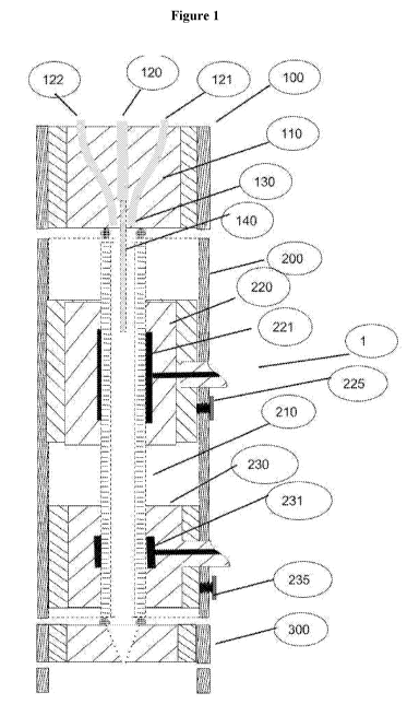
[00115] Figure 1 provides a cross-section view of an exemplary print head 1.
In some
embodiments, the print head 1 comprises an inlet manifold 100. In some
embodiments, the
print head 1 comprised a plasma manifold 200. In some embodiments, the print
head 1
comprises a nozzle manifold 300. In some embodiments, the print head
lcomprises a
modular assembly comprising an inlet manifold 100, a plasma manifold 200, a
nozzle
manifold 300, or a combination thereof. A modular assembly can allow the
different
manifolds to be dismantled and connected together as needed, depending on the
required
plasma characteristic and the type/quality of materials being printed.
[00116] In some embodiments, the inlet manifold 100 comprises a dielectric
material to
create a dielectric inlet manifold 110. In some cases, the dielectric material
comprises
ceramics. In some cases, the dielectric material comprises aluminum oxide,
polyether ether
ketone (PEEK), polytetrafluoroethylene (PTFE).
[00117] In some embodiments, the dielectric inlet manifold 110 comprises one
or more
inlets. The one or more inlets provide for the entry of one or more materials.
In some cases,
the one or more materials comprise a gas. In some cases, the gas comprises
helium, argon,
hydrogen, nitrogen, or a combination thereof In some cases, the one or more
materials
comprise a metallic colloid. In some cases, the metallic colloid comprises a
copper
nanomaterial, a silver nanomaterial, a gold nanomaterial, or a combination
thereof In some
11
CA 03076753 2020-03-23
WO 2019/068070 PCT/US2018/053703
cases, the one or more materials comprise a precursor material. In some cases,
the precursor
material comprises an organic precursor. In some cases, the organic precursor
comprises
hexamethyldisiloxane, tetraethyl orthosilicate, (3-amino propyl)triethoxy
silane, or a
combination thereof In some cases, the dielectric inlet manifold 110 comprises
three inlets
120, 121, and 121.
[00118] In some embodiments, the inlet manifold 100 is connected to the plasma
manifold
200. In some cases, the dielectric inlet manifold comprises an opening 130.
The opening 130
may allow a primary dielectric tube 210 of the plasma manifold 200 to connect
with the inlet
manifold 100. In other cases, one of the inlets 120 can connect with an
optional secondary
dielectric tube 140. In those cases, the dielectric tube 140 can have a
variable length. The
length of the dielectric tube 140 can depend on the nature and the type of
material to be
printed. In some cases, the secondary dielectric tube 140 ends before the
beginning of the one
or more electrodes 221of the plasma manifold 200. In some cases, the secondary
dielectric
tube 140 extends beyond electrode 221 and ends before the beginning of
electrode 231. In
some cases, the secondary dielectric tube 140 extends beyond electrode 231. In
some cases,
the secondary dielectric tube 140 extends to the nozzle manifold 300.
[00119] Figure 2 is a cross sectional view of the exemplary inlet manifold
100. In this
exemplary embodiment, the dielectric inlet manifold 110 comprises three inlets
120, 121, and
122. Figure 2 also provides an optional secondary dielectric tube 140.
[00120] Figure 3 is a cross sectional view of an exemplary plasma manifold
220. In some
embodiments, the plasma manifold 220 comprises one or more electrodes. In the
exemplary
embodiment of Figure 3, the plasma manifold 220 comprises two or more
electrodes 221,
231 that could be moved along a circumference of a primary dielectric tube
210. In some
embodiments, the electrodes 221 and 231 can contain one or more dielectric
enclosures 222
and 232 and an outer shield 223 that connect all the three major portions of
the modular print
head 1, namely inlet module 100, plasma module 200 and nozzle module 300. In
Figure 3,
the plasma module 200 can contain an electrical feedthrough 224 that is
connected to the
electrode 221 with dielectric encapsulation 222. The electrodes 221 and 231 in
the plasma
manifold are fixed to the primary dielectric tube 210 using an adjustable
mechanical position
controller 225 and 235. The position controller can be a screw, slide or be
made of any
adjustable fixture, and can be moved along the axis of the primary dielectric
tube 210 by
manual or by using a mini motor. The spacing between electrodes 221 and 231
(shown in
Figure 1) can be controlled using the position controller 225 and 235
depending on the
12
CA 03076753 2020-03-23
WO 2019/068070 PCT/US2018/053703
nature and type of materials being printed and the plasma characteristics
required to obtain
molecular precision in printing.
[00121] Figure 4 provides exemplary cross sectional views of a plasma module
200,
comprising one or more electrodes. The one or more electrodes can be connected
to high
voltage power supply. Different configurations of electrodes are shown in
Figure 4 with
varying electrode spacing and surface area. Figure 4A shows bottom electrode
231
connected to ground and electrode 221 connected to high voltage. In this
embodiment, the
secondary dielectric ends before the top electrode. Figure 4B shows an
additional electrode
141 dispersed along the circumference of the secondary inner dielectric 140.
Figure 4C
shows the electrode 371 placed outside the print head, connected to ground
while the two
electrodes 221 and 141 are connected to high voltage. Figure 4D shows that the
bottom
electrode 231 is connected to ground and top electrode 221 is connected to
high voltage while
the length of the secondary dielectric 140 is extended till the bottom
electrode 231. Figure
4E shows a ring electrode 221 connected to high voltage power supply.
[00122] Figure 5 provides an exemplary gradient plasma setup with an
illustrative primary
dielectric tube 210 comprising one or more electrodes 221a, 221b, 231a, and
231b. The one
or more electrodes can be connected to power supplies which can be
independently
controlled to create a gradient plasma and a temperature gradient in the
primary dielectric
tube.
[00123] Figure 6 provides cross sectional view of an exemplary modular print
head
comprising an inlet module and a plasma module. The print head can comprise a
primary
dielectric tube 210 and an optional secondary dielectric tube 140. The length
of the optional
secondary dielectric tube 140 whose length can be varied depending on the
application so that
the material coming out of secondary dielectric tube is either exposed to the
entire plasma
region comprising two or more electrodes or to a partial plasma region or to a
glow discharge
region of the plasma close to the nozzle
[00124] Figure 7A is a cross sectional view of an exemplary nozzle module 300.
In some
embodiments, the nozzle module 300 can be attached to the primary dielectric
tube 210 of the
plasma module 200. In some embodiments, the nozzle module 300 comprises a
nozzle with
an orifice 330. In some cases, the inner diameter of the orifice 310 can be
controlled and
varied as needed depending on the application and type/nature of material
being printed. In
some cases, the diameter of the orifice 330 of the nozzle is the same at the
inner diameter of
the orifice 310. In other cases, the diameter of the orifice 330 is smaller
than the inner
diameter of the orifice 310.
13
CA 03076753 2020-03-23
WO 2019/068070 PCT/US2018/053703
[00125] In some embodiments, the nozzle module 300 comprises of a dielectric
material
322. In some cases, the dielectric material 322 is surrounded by an outer
shield 323. In some
cases, the outer shield 323 can be connected electrically to ground. In some
cases, a
protective enclosure or housing 324 can be used to connect the nozzle module
to the plasma
module 200 to complete a modular dielectric print head assembly.
[00126] Figure 7B provides an exemplary illustration of a discharge 351 from
the orifice
330 of the nozzle module.
[00127] Figure 7C provides an exemplary embodiment of a nozzle module
comprising a
gas inlet 360. In some cases, a gas 361 provided through the gas inlet 360 can
be used to
focus any material exiting the plasma module. In some cases, the gas 361
provided through
the gas inlet 360 can tailor one or more properties of the material in the
discharge 351 at the
glow discharge region.
[00128] Figure 8A is an exemplary schematic of printing using the nozzle
module of the
modular print head. The exemplary embodiment comprises printing using a
sacrificial orifice
or mask 350, to print on a substrate 353 with precise geometry of printed
material 352. The
plasma glow discharge region containing the material 351 is directed out of
the nozzle
module 300 for printing with a geometry of interest, a resolution of interest,
or a combination
thereof. Printing with a high resolution, a high precision, or a combination
thereof, can be
achieved by using a sacrificial mask 350. In some embodiments, the diameter of
the orifice or
opening of the sacrificial mask 350 is smaller than the orifice opening 330 of
the nozzle
module 300. In some embodiments, the diameter of the orifice or opening of the
sacrificial
mask 350 is about the same as the orifice opening 330 of the nozzle module
300. In some
embodiments, the diameter of the orifice or opening of the sacrificial mask
350 is greater than
the orifice opening 330 of the nozzle module 300.
[00129] In some embodiments, the sacrificial orifice or mask 350a as shown in
Figure 8B
can be indexed when deposition builds up. In some embodiment, the sacrificial
orifice or
mask 350a can be indexed for different shape.
[00130] In some cases, the quality of printing may be disrupted. For example,
an orifice in
sacrificial mask may become clogged; or deposition may build up on the
sacrificial mask. In
those cases, the sacrificial orifice or mask 350 can be adjusted or replaced
to get a new
unclogged orifice.
[00131] In some cases, two or more different patterns may be required for
printing. In those
cases, the sacrificial orifice or mask 350 can be adjusted or replaced to get
a new pattern
depending on the need.
14
CA 03076753 2020-03-23
WO 2019/068070 PCT/US2018/053703
[00132] In some embodiments, the sacrificial orifice or mask 350 comprises one
or more
orifices or patterns. Figure 9 shows examples of different shaped sacrificial
orifices or
patterned masks 350 a, 350b, 350c, and 350d. The patterned masks and the
sacrificial orifices
could be made of any material including metals, dielectric materials, silicon,
plastic, or a
combination. The patterned masks and sacrificial orifices could be made using
any of the
known methods including laser etching, wet etching, plasma etching,
lithography process, or
a combination thereof.
[00133] Figure 10A is a photograph of an exemplary modular print head
comprising an inlet
manifold, a plasma manifold and a nozzle manifold. In this exemplary
embodiment, the print
head comprises an electrode, a dielectric encapsulation of the electrode, a
primary dielectric
tube, and an electric feedthrough to the electrode. Figure 10B is a photograph
of an
exemplary modular print of a different configuration. In this embodiment, the
print head
comprises ashort electrode spacing.
[00134] Figure 11A and Figure 11B provide photographs of an exemplary modular
print
head with the plasma ON.
[00135] Figure 12A is a photograph of an exemplary print head without the
nozzle manifold
with plasma ON. Figure 12B is a photograph of an exemplary print head with an
electrically
grounded shield that can be touched safely during the operation of the plasma
jet printer.
[00136] The primary dielectric tube 210 could be made of any dielectric
material not
limited to ceramic, inorganic materials, including alumina, quartz, teflon,
silica, aluminum
oxide, or a combination thereof.
[00137] The dielectric enclosure 222 and encapsulation shield 232 used to
enclose the
electrodes 221 and 231 could be made of any insulating materials, ceramics,
inorganic
materials or mixtures not limited to teflon, macor, alumina, or a combination
thereof. Arcing
in plasma is a common phenomenon. Total dielectric strength of encapsulated
dielectric is
higher than that of the dielectric tube on which electrodes are placed.
[00138] The electrodes and electrical feed throughs could be made of any
metal, alloy that
conducts electricity including but not limited to copper and stainless steel.
[00139] Printing of materials using plasma jet require the precursor or actual
material to be
printed be introduced in to the plasma jet print head comprising dielectric
tube, electrodes
connected to high voltage power supply, gas supply and a nozzle through which
the
introduced material is directed towards the substrate on to which the material
is to be printed.
[00140] The precursor or actual material to be introduced into the plasma jet
print head can
be in the form of dry particles or aerosolized particles or aerosolized
solution that enters the
CA 03076753 2020-03-23
WO 2019/068070 PCT/US2018/053703
region where active plasma is sustained for sufficient chemical or physical or
electronic or
molecular or morphological change and are directed to be printed on the
substrate. The
precursor or actual material may also be introduced into the plasma jet print
head in the form
of controlled size droplets or controlled volume liquid or paste dispense.
[00141] The precursor or actual material to be printed can also be introduced
in the glow
discharge region of the plasma by avoiding interaction of the material with
active plasma
region and hence retaining the pristine material characteristics. For this
purpose, the material
to be printed can be introduced through secondary dielectric tube.
[00142] Plasma jet printing of materials with tailored material
characteristics and defined
geometry on a wide range of 2D, 3D objects and soft, or hard substrates and
for
manufacturing in a reliable, reproducible and high throughput fashion requires
a print head
that can sustain a stable plasma with several key features including ability
to control the
plasma characteristics through which printed material characteristics can be
tailored; with the
ability to print materials with user defined resolutions, ability to avoid
plasma arc between
the print head components, electrodes, substrate, substrate holder, printed
material etc.,
ability to sustain temperature gradient in print head for printing materials
with varying
temperature allowing the operating temperature of the substrate to vary from
20 C to several
hundred degree Celsius.
[00143] In one configuration, the ability to print materials with printed
geometries between
50 nm and 500um with control over the repeatability and accuracy of the
resultant geometry
is provided. In another configuration, the ability to print materials with
printed geometries of
between 500um and 10cm is provided. In another configuration, the ability to
print materials
with printed geometries of between 10cm and 50cm is provided. Similarly, the
ability to treat
materials and substrates with plasma for all the above defined geometry ranges
is provided.
Some configuration allows use of multiple print heads simultaneously to print
and treat
materials on a large area.
[00144] The ability to print a variety of materials with controlled but
variable morphologies
including amorphous, agglomerated particle, porous continuous or non-
continuous is
provided.
[00145] The ability to precisely control the printed material rate of
deposition and thickness
of deposition during printing by means of manipulating the plasma
characteristics and/or the
delivery of the material being printed is provided.
[00146] Printing materials using plasma jet with defined geometry and tailored
material
characteristics including physical, chemical, mechanical, electronic, optical,
bio-interface,
16
CA 03076753 2020-03-23
WO 2019/068070 PCT/US2018/053703
biocompatible properties require optimum plasma characteristics to obtain any
one or more
combination of above mentioned material properties. For example, nature and
type of plasma
gas, plasma density, electron temperature, ion temperature, free radical
generation, available
volume between electrodes, electrode configuration, number of active
electrodes etc., can
play a significant role in printing materials with any of the required
properties including
physical, chemical, mechanical, electronic, magnetic, optical, bio-interface,
biocompatible
properties etc.,
[00147] A plasma jet printer is disclosed, that can print wide range of
materials on wide
range of substrates including 2D, 3D, hard, soft, continuous, porous,
flexible, rigid, vials,
wells etc., can be used in manufacturing in various fields including
electronics, textiles,
medical, wearable, automobile, aerospace, energy storage/generation, display,
food
packaging, sensors, implants, test equipment etc.,
[00148] Printing a wide range of materials with unique material characteristic
for any or all
field of use application requires appropriate precursor materials, appropriate
substrate,
appropriate processing environment like humidity, temperature, pre-treatment
of substrate,
masks, printing, post-treatment, curing etc.
[00149] However, plasma jet printing of wide range of materials with tailored
material
characteristics requires a key component, namely a controlled plasma
environment that can
change, modify or control the properties of the material that goes through the
plasma region
or retain those properties depending on the need. Say for example, printing of
conducting
materials will require prevention of oxidation, reduction of materials in-situ
or post printing,
partial or full melting of materials, etc., For printing of organic coatings,
polymerization is
essential. For printing of organic electronics or chemicals or drugs,
retaining of chemical
structure is essential. For printing of dielectric coatings with varying
dielectric strength, the
chemical composition needs to be varied. For printing biocompatible coatings,
retaining the
chemical structure of drugs is essential.
[00150] For printing of organics, inorganics, metals, metal oxides,
semiconductors,
magnetic materials, ceramics, polymers, drugs, chemicals, small organic
molecules, big
organic molecules, or a combination, the plasma characteristics in the print
head and the gas
composition, precursor composition will have to be precisely controlled.
Though the
precursor composition and gas composition can easily be controlled with
appropriate use of
ink cartridge and gas supply line, controlling the plasma characteristics for
printing require
optimal configuration of several key components including dielectric strength
of the
dielectric print head and the tube thickness, electrode configuration,
electrode spacing,
17
CA 03076753 2020-03-23
WO 2019/068070 PCT/US2018/053703
dielectric encapsulation of electrodes, volume of the portion of dielectric
tube that contains
the active plasma region, number of live/ground/floating electrodes, nature
and type of
nozzle, orifice diameter in nozzle, particle feeding rate etc.,
[00151] Modular design of the print head with multiple feed throughs for
precursor and gas
inlet, multiple dielectric tubes connected through a manifold and placed
inside the main
dielectric tube containing electrodes in which the plasma is generated,
adjustable electrode
spacing, replaceable nozzles with varying orifice diameter for printing,
provision to increase
or decrease the total number of electrodes in the print head, dielectric
encapsulation of
electrodes, uneven electrode areas can all play a significant role in deciding
the optimum
parameters needed for printing specific class of materials, the quality of the
printed material
as well as the nature of material that can be printed.
[00152] For example, a modular design of the print head that is optimized for
printing 10
microns thick uniform conducting metallic features with defined line
resolution (say 50
microns) from the corresponding metal oxide input, will allow increased
dwelling time of
metallic particles in the plasma containing reducing gas environment and also
higher
temperature in specific regions of the dielectric tube. The number of
electrodes, electrode
spacing, plasma volume, particle/aerosol/precursor feeding, nature and type of
nozzle, orifice
diameter, applied potential will have to be optimized to obtain a plasma
characteristic that
will make maximum use of plasma parameters/properties to reduce metal oxide to
metal and
also to partially or fully melt metallic input to form a continuous metal film
with precise 50
microns conducting metallic line feature.
[00153] However, a modular design of the print head for printing a 10
nanometer thick
organic polyethylene glycol coating with a line width of 5 millimeters on a
biosensor or
medical device will have the electrode design in such a way that the plasma
characteristics
are not too intense to damage the chemical structure of the precursor or the
substrate and at
the same time enabling plasma polymerization to take place. The number of
electrodes,
electrode spacing, plasma volume, particle/aerosol/precursor feeding, nature
and type of
nozzle, orifice diameter, applied potential will be optimized for this
application and the
parameters will be different than that of printing metal from metal oxides
with fine feature.
[00154] The idea behind the modular design of the plasma jet print head is to
allow
optimization of the print head design, configuration and process parameters
for specific
application.
18
CA 03076753 2020-03-23
WO 2019/068070 PCT/US2018/053703
[00155] Also the modular design of the plasma jet print head enables
integration of the
print head to other printing techniques like aerosol jet printing, spray
pyrolysis, ink jet
printing, laser printing, drop casting etc.,
[00156] Use of high voltage power supply is essential for generating
plasma
discharge. The high voltage is applied between the electrodes in the
dielectric tube of plasma
jet print head. The nature and type of power input can vary from DC, pulsed
DC, AC to RF.
The power supply can either be battery powered or connected to a high voltage
source. Use
of multiple electrodes in the same print head will allow application of
varying input energy to
selected electrodes resulting in gradient plasma in the dielectric tube.
[00157] A modular design with two electrodes in the print head could result
in uniform
plasma. However, in a modular design with an elongated dielectric tube with
four electrodes
in the print head, two electrodes could be connected to a power supply with
higher input
energy and two other electrodes could be connected to the same or different
power supply
with lower input energy than the other electrodes. In this case, the plasma
characteristics in
higher input region is likely to be have a higher ion energy, electron/ion
temperature, plasma
density etc., than that of the lower energy input region. This design can be
used to introduce
temperature gradient in the print head and for increased dwelling time of the
materials in the
plasma. Both the electrode sets could also be connected to similar potential
resulting in
uniform plasma across the entire print head.
[00158] Use of high voltage power supply and generation of plasma can also
result in
arcing between the metallic components of the print head or the printer
assembly. The arcing
can happen between the electrodes of the print head, the plasma and the
substrate or substrate
holder, or the metallic coating being printed. The modular design of the
plasma jet print head
assembly provides a solution to avoid arcing during the printing and post-
printing.
[00159] The modular design of the plasma jet print head comprise a manifold
connected to
the primary dielectric tube on which electrodes connected to high voltage
power supply are
dispersed. The manifold will have provision for gas input and
precursor/material inlet and a
provision to connect dielectric tubes from the gas input and/or
precursor/material input inside
the primary dielectric tube whose length can be controlled depending on the
application. The
inner dielectric tubes placed inside the primary dielectric tube can carry the
precursor or gas
or both. The modular design also allows the provision to have a manifold with
inlets for gas
and precursor without multiple dielectric tubes and containing only the
primary dielectric
tube inside which both the gas and precursor/material are introduced.
19
CA 03076753 2020-03-23
WO 2019/068070 PCT/US2018/053703
[00160] The length and diameter of the primary dielectric tube in the modular
design can be
varied depending on the nature and type of material to be printed and the
application. The
thickness, dielectric strength and diameter of the dielectric tube can vary
the plasma
characteristics and the temperature inside the tube allowing for tailoring the
material
properties of the printed features/structures. The modular design allows
joining of two or
more dielectric tubes that are similar or of varying diameters along the
longitudinal axis.
[00161] In some embodiments, the diameter of the dielectric tube is about 0.02
cm to about
2 cm. In some embodiments, the diameter of the dielectric tube is at least
about 0.02 cm. In
some embodiments, the diameter of the dielectric tube is at most about 2 cm.
In some
embodiments, the diameter of the dielectric tube is about 0.02 cm to about
0.05 cm, about
0.02 cm to about 0.1 cm, about 0.02 cm to about 0.5 cm, about 0.02 cm to about
1 cm, about
0.02 cm to about 1.5 cm, about 0.02 cm to about 2 cm, about 0.05 cm to about
0.1 cm, about
0.05 cm to about 0.5 cm, about 0.05 cm to about 1 cm, about 0.05 cm to about
1.5 cm, about
0.05 cm to about 2 cm, about 0.1 cm to about 0.5 cm, about 0.1 cm to about 1
cm, about 0.1
cm to about 1.5 cm, about 0.1 cm to about 2 cm, about 0.5 cm to about 1 cm,
about 0.5 cm to
about 1.5 cm, about 0.5 cm to about 2 cm, about 1 cm to about 1.5 cm, about 1
cm to about 2
cm, or about 1.5 cm to about 2 cm. In some embodiments, the diameter of the
dielectric tube
is about 0.02 cm, about 0.05 cm, about 0.1 cm, about 0.5 cm, about 1 cm, about
1.5 cm, or
about 2 cm.
[00162] The electrodes that will be connected to a voltage source are
dispersed along the
primary dielectric tube. The number of electrodes can be two or more and the
surface area of
one of the electrodes is more than double that of the second electrode. The
electrodes can
either be placed along the outer circumference of the dielectric tube, or one
of the electrodes
can be placed inside the dielectric tube and the other along the outer
circumference, or the
electrodes can be embedded inside the dielectric tube such that the portion of
electrodes are
exposed to the inner portion of the dielectric tube.
[00163] One or all of the electrodes can either be similar in shape or more
than one can be of
any shape like that of a planar tape or wire like winding along the
circumference or pointed
edge or sharp blade like when embedded inside the dielectric or one of the
electrodes can be
rod shaped and placed inside the dielectric. However, in all these cases
except for electrodes
that are embedded inside the dielectric, the electrode separation distance can
be changed
depending on the required configuration/application/quality of printing and
the electrodes
dispersed along the circumference of the dielectric are movable along the
longitudinal axis.
CA 03076753 2020-03-23
WO 2019/068070 PCT/US2018/053703
[00164] In some embodiments, the distance between the first electrode and
the second
electrode is about 5 mm to about 40 mm. In some embodiments, the distance
between the
first electrode and the second electrode is at least about 5 mm. In some
embodiments, the
distance between the first electrode and the second electrode is at most about
40 mm. In some
embodiments, the distance between the first electrode and the second electrode
is about 5 mm
to about 10 mm, about 5 mm to about 15 mm, about 5 mm to about 20 mm, about 5
mm to
about 25 mm, about 5 mm to about 30 mm, about 5 mm to about 35 mm, about 5 mm
to
about 40 mm, about 10 mm to about 15 mm, about 10 mm to about 20 mm, about 10
mm to
about 25 mm, about 10 mm to about 30 mm, about 10 mm to about 35 mm, about 10
mm to
about 40 mm, about 15 mm to about 20 mm, about 15 mm to about 25 mm, about 15
mm to
about 30 mm, about 15 mm to about 35 mm, about 15 mm to about 40 mm, about 20
mm to
about 25 mm, about 20 mm to about 30 mm, about 20 mm to about 35 mm, about 20
mm to
about 40 mm, about 25 mm to about 30 mm, about 25 mm to about 35 mm, about 25
mm to
about 40 mm, about 30 mm to about 35 mm, about 30 mm to about 40 mm, or about
35 mm
to about 40 mm. In some embodiments, the distance between the first electrode
and the
second electrode is about 5 mm, about 10 mm, about 15 mm, about 20 mm, about
25 mm,
about 30 mm, about 35 mm, or about 40 mm.
[00165] In some embodiments, the distance between the electrodes is about 1
mm to
about 180 mm. In some embodiments, the distance between the electrodes is at
least about 1
mm. In some embodiments, the distance between the electrodes is at most about
180 mm. In
some embodiments, the distance between the electrodes is about 1 mm to about
10 mm, about
1 mm to about 25 mm, about 1 mm to about 50 mm, about 1 mm to about 75 mm,
about 1
mm to about 100 mm, about 1 mm to about 125 mm, about 1 mm to about 150 mm,
about 1
mm to about 180 mm, about 10 mm to about 25 mm, about 10 mm to about 50 mm,
about 10
mm to about 75 mm, about 10 mm to about 100 mm, about 10 mm to about 125 mm,
about
mm to about 150 mm, about 10 mm to about 180 mm, about 25 mm to about 50 mm,
about 25 mm to about 75 mm, about 25 mm to about 100 mm, about 25 mm to about
125
mm, about 25 mm to about 150 mm, about 25 mm to about 180 mm, about 50 mm to
about
75 mm, about 50 mm to about 100 mm, about 50 mm to about 125 mm, about 50 mm
to
about 150 mm, about 50 mm to about 180 mm, about 75 mm to about 100 mm, about
75 mm
to about 125 mm, about 75 mm to about 150 mm, about 75 mm to about 180 mm,
about 100
mm to about 125 mm, about 100 mm to about 150 mm, about 100 mm to about 180
mm,
about 125 mm to about 150 mm, about 125 mm to about 180 mm, or about 150 mm to
about
180 mm. In some embodiments, the distance between the electrodes is about 1
mm, about 10
21
CA 03076753 2020-03-23
WO 2019/068070 PCT/US2018/053703
mm, about 25 mm, about 50 mm, about 75 mm, about 100 mm, about 125 mm, about
150
mm, or about 180 mm.
[00166] The electrodes are part of the modular design of the print head in
which the
number, size and spacing of the electrodes can be easily changed providing an
opportunity to
control plasma characteristics through application specific, precise
configuration of
electrodes for reliable and reproducible printing of materials with tailored
characteristics.
Generating plasma using multiple electrodes dispersed along the dielectric and
applying
similar or varying potentials to various sets of electrodes can create a
gradient in plasma
characteristics. In some cases, a temperature gradient is created which will
drastically change
the material properties such as increasing dwelling of materials in the plasma
zone and
resulting in change of electronic or mechanical or optical or chemical
properties of the
resultant printed feature.
[00167] The provision to change spacing between the electrodes provides the
opportunity to change plasma characteristics and hence the quality of
materials printed. For
example, two electrodes dispersed along the outer circumference of the
dielectric tube with 1
centimeter spacing between them will have a certain plasma characteristics for
a given
externally applied electric potential. However, for the same potential, if the
electrode spacing
is increased to 2 centimeters the plasma characteristics will be different and
higher potential
will be required to ignite and sustain the plasma. The quality of films
printed under the two
configurations could vary significantly for a given set of fixed plasma
process parameters like
flow rate, applied voltage, printing time, or a combination thereof
[00168] Changing the spatial distribution of electrodes to print materials
allows
changing parameters like thermal energy in the plasma, electron and ion
density in the
plasma, bombardment between various species in the plasma and the material to
be printed,
and also momentum transferred on to the materials and substrate during
printing. A plasma
jet print head with safe option to change the electrode spacing in a single
step process without
having to remove the electrode from the print head offers a unique capability
to tune the
properties of the materials printed using the plasma jet print head.
[00169] The print head described herein can connect multiple electrodes in
a confined
zone and without any electrical arc between any of the internal components of
the print head
or with the substrate or with the substrate holder or with the material being
printed. An
apparatus for printing materials using plasma jet in a defined geometry with a
modular print
head design comprising detachable dielectric tubes, metal electrodes and
dielectric
22
CA 03076753 2020-03-23
WO 2019/068070 PCT/US2018/053703
encapsulations that avoids arcing between electrodes, substrate, substrate
holder, coated
material for printing materials with tailored material properties is
disclosed.
[00170] The modular design of the plasma jet print head allows for
attaching dielectric
tubes along the longitudinal axis that can be used for focusing the materials
towards substrate
for printing. The ability to increase, decrease, narrow or widen the length,
diameter and
volume of the dielectric tube provides an opportunity to change the plasma
volume and in
turn tune the interaction of the material to be printed with the plasma.
[00171] The modular design of the plasma jet print head allows for
attaching or
removing a replaceable nozzle with defined orifice diameter that can be used
for printing
required feature size and resolution. The orifice diameter can either remain
the same as the
dielectric tube or it can be narrowed to suit the required resolution varying
from 5 centimeters
to 5 microns to further down to submicron level to 50nm with the use of
silicon micro-
machined nozzle. In another configuration, large area coating could be
achieved by having
multiple dielectric tubes or print heads for simultaneous printing or use of
larger diameter
orifice greater than 5cm.
[00172] The narrow orifice and design of the nozzle along with the
externally applied
electric field and presence of plasma helps driving the material entering the
dielectric tube to
get focused and accelerated towards the substrate enabling high resolution and
high
throughput printing.
[00173] The modular design of the print head also allows the introduction
of an inert or
higher dielectric strength gas (than the ones used for generating plasma) at
the nozzle as a
sheath gas for focussing the material towards the substrate.
[00174] The nozzle that can be easily replaced and also attached to the
primary dielectric
tube can comprise a plain dielectric material with an orifice or be designed
with a
continuously narrowing inner dimension to allow for fine resolution printing
or contain a
metal inside or at the edge that can either be at floating potential or
connected to ground. The
presence of metal at the nozzle can play a significant role in reducing arcing
between the
plasma in the print head and substrate or substrate holder or the material
being printed.
[00175] Arcs in plasma and high voltage are a common phenomenon. However,
for
printing application arcing should be avoided as it can damage the substrate
or the
components of the print head. The modular design of the print head allows a
stable arc-less
plasma to sustain and prevent arcing between the electrodes or arcing between
the plasma and
substrate or substrate holder or material being printed.
23
CA 03076753 2020-03-23
WO 2019/068070
PCT/US2018/053703
[00176] Applying high voltage to electrodes placed along the circumference
of the
dielectric tube can cause arcing either external to the dielectric, here after
called as external
arcing, or internal to the dielectric tube, here after called as internal
arcing, or both. For
printing applications, both internal and external arcing between the
electrodes should be
prevented.
[00177] The modular design of the print head incorporates multiple features
that prevent
arcing between the electrodes or arcing between the plasma and the electrodes
in the print
head. One of the ways to prevent arcing is to use uneven surface area of
electrodes. Another
way is to use thicker dielectric encapsulation of electrodes so that the
electrodes are not
exposed to ambient environment.
[00178] With
the electrodes dispersed along the circumference of the dielectric tube,
one of the electrodes has a surface area more than double that of the other
electrode, such that
the electric field is spread over a larger area, minimizing arcing.
[00179] A key feature to prevent arcing between electrodes that are dispersed
along the
outer circumference of the dielectric tube is to encapsulate the electrodes
with dielectric
material whose thickness is more than thrice that of the thickness of the
primary dielectric
tube on which the electrodes are dispersed. The total dielectric strength of
the encapsulated
dielectric is higher than that of the primary dielectric tube on which the
electrodes are
dispersed.
[00180] The
carrier gas that carries the aerosolized material to be printed and the gas
that
is used to generate plasma discharge can either be same or different depending
on the nature
of the material and the required resultant printed material properties. In the
case where the
effect of plasma species on the materials is to be minimized and restricted to
a minimal
region containing plasma, a non-interactive higher dielectric strength carrier
gas can be used
to transfer the material and a gas with lower dielectric strength like that of
argon or helium be
used to generate plasma discharge. The higher dielectric strength carrier gas
can also be used
as a focusing gas at the nozzle and the modular design allows feeding the
required gas
mixtures either at the input manifold of the print head or closer to the
electrode in the
dielectric tube or at the nozzle.
[00181] The
modular design of the print head that allows connecting multiple electrodes
(more than 2) in the dielectric tube, provision to control the plasma volume
and the
interaction time of plasma species with the materials and provision to
introduce required gas
mixture in any portion of the dielectric tube like that of inlet manifold,
before or in between
24
CA 03076753 2020-03-23
WO 2019/068070
PCT/US2018/053703
or after the electrodes allows intricate control of the plasma characteristics
and in turn allows
tailoring of the material properties resulting in printing of custom made
material.
[00182] Multiple electrodes powered with varying input energies for
generating
plasma with either the same gas mixture or different gas mixtures allow dual
plasma zones in
the primary dielectric tube as shown in Figure 5. The region inside the
dielectric tube has
different plasma characteristics in each plasma zone. For example plasma zone
1 with higher
input electric energy across the electrodes 221a and 221b can have higher
temperature and
plasma zone 2 with lower input electric energy across the electrodes 231a and
231b can have
lower temperature. Plasma zone 1 inside the primary dielectric tube between
the electrodes
221a and 221b can have reducing environment and plasma zone 2 between the
electrodes
231a and 231b can have inert environment. This allows intricate control of
both temperature
driven and chemically driven modification of the printed material. Plasma zone
2 can act as a
focusing or a cooling unit while still maintaining an active plasma region
enabling printing on
low glass transition materials.
[00183]
Plasma zone 1 provide optimal conditions for chemical, electronic, magnetic,
structural or morphological modification of the material, plasma zone 2 can
remain optimized
for best printing properties depending on the substrate, temperature,
adhesion, pre-treatment,
post-treatment etc., requirement.
[00184] The print head can generate atmospheric pressure plasma that
directs and
prints materials onto the substrate where the substrate temperature during the
printing process
can vary from as low as 20 C to as high as 300 C as determined by the
electrode
configuration, electrode spacing, applied power, dielectric tube, nature of
gas, to name a few.
In some cases, the substrate temperature is about 20 C to about 300 C. In
some cases, the
substrate temperature is at least about 20 C. In some cases, the substrate
temperature is at
most about 300 C. In some cases, the substrate temperature is about 20 C to
about 50 C,
about 20 C to about 75 C, about 20 C to about 100 C, about 20 C to about
125 C, about
20 C to about 150 C, about 20 C to about 175 C, about 20 C to about 200
C, about 20 C
to about 225 C, about 20 C to about 250 C, about 20 C to about 275 C,
about 20 C to
about 300 C, about 50 C to about 75 C, about 50 C to about 100 C, about
50 C to about
125 C, about 50 C to about 150 C, about 50 C to about 175 C, about 50 C
to about 200
C, about 50 C to about 225 C, about 50 C to about 250 C, about 50 C to
about 275 C,
about 50 C to about 300 C, about 75 C to about 100 C, about 75 C to about
125 C, about
75 C to about 150 C, about 75 C to about 175 C, about 75 C to about 200
C, about 75 C
to about 225 C, about 75 C to about 250 C, about 75 C to about 275 C,
about 75 C to
CA 03076753 2020-03-23
WO 2019/068070 PCT/US2018/053703
about 300 C, about 100 C to about 125 C, about 100 C to about 150 C,
about 100 C to
about 175 C, about 100 C to about 200 C, about 100 C to about 225 C,
about 100 C to
about 250 C, about 100 C to about 275 C, about 100 C to about 300 C,
about 125 C to
about 150 C, about 125 C to about 175 C, about 125 C to about 200 C,
about 125 C to
about 225 C, about 125 C to about 250 C, about 125 C to about 275 C,
about 125 C to
about 300 C, about 150 C to about 175 C, about 150 C to about 200 C,
about 150 C to
about 225 C, about 150 C to about 250 C, about 150 C to about 275 C,
about 150 C to
about 300 C, about 175 C to about 200 C, about 175 C to about 225 C,
about 175 C to
about 250 C, about 175 C to about 275 C, about 175 C to about 300 C,
about 200 C to
about 225 C, about 200 C to about 250 C, about 200 C to about 275 C,
about 200 C to
about 300 C, about 225 C to about 250 C, about 225 C to about 275 C,
about 225 C to
about 300 C, about 250 C to about 275 C, about 250 C to about 300 C, or
about 275 C to
about 300 C. In some cases, the substrate temperature is about 20 C, about
50 C, about 75
C, about 100 C, about 125 C, about 150 C, about 175 C, about 200 C, about
225 C,
about 250 C, about 275 C, or about 300 C.
[00185] The modular design of the print head has the provision to
introduce
precursor, gas or other material to the print head in more than one way to get
tailor-made
material properties and or materials with pristine properties as in the
original precursor. This
can be achieved by having plurality of inputs and/or dual dielectric tubes.
[00186] The print head input manifold may have one input for the precursor
and gas, or
one input for both precursor and gas, to enter into the primary dielectric
tube. The manifold
may also have plurality of inputs for more than one precursor, or gases, to
enter the primary
dielectric tube, either one at a time or simultaneously.
[00187] The modular design of the print head allows for one or more inputs
for the
precursors, or gases, to enter into the primary dielectric tube and there may
be a secondary
dielectric tube within the primary dielectric tube. In this configuration, the
precursors may
enter into either the primary or secondary dielectric tube, or both, one at a
time or
simultaneously. The electrodes in this configuration are present in outer
dielectric tube and
the length of the inner dielectric tube can vary. The length of the inner
secondary dielectric
tube can either be same as the outer primary dielectric tube or shorter. The
length of the
inner secondary dielectric tube can be varied in such a way that the
dielectric tube can end
well before the electrode placed at the outer primary dielectric or stretch
all the way unto the
nozzle or take any intermediary length independent of the length of the
primary dielectric
tube.
26
CA 03076753 2020-03-23
WO 2019/068070 PCT/US2018/053703
[00188] Depending on the gas constituent and or precursor/material input
from the
primary dielectric and the length of the secondary dielectric placed inside
the primary, the
precursor/material or gas introduced through the secondary dielectric can
either face the
active plasma region created by the electrodes dispersed over the primary
dielectric tube or
face only the glow discharge region of the place at the nozzle or at the exit
of the nozzle. This
allows the materials introduced through the secondary dielectric tube to
either undergo
plasma induced property changes or maintain its pristine characteristics
without undergoing
plasma induced structural, chemical or material property changes.
[00189] The modular design of the print head allows for multiple
dielectric tubes to be
present with provision for including one or more secondary dielectric tubes
within the
primary dielectric tube. The inputs to the primary and the secondary
dielectric tubes can
again be independently controlled and also the length of all or any of the
secondary dielectric
tube can either be same as primary dielectric tube or shorter than the primary
dielectric tube.
[00190] The modular assembly of the print head allows for further
improving the
resolution by placing a patterned focusing apparatus with a defined orifice
whose opening is
smaller than the orifice of the nozzle. The modular design allows for the
utilization of a
patterned or controlled geometry sacrificial mask to print though, providing
an additional
means for transferring a precise pattern to the substrate or further refining
the geometry of the
print by restricting the area of the substrate exposed to the print medium.
This may be as
simple as an additional orifice that is smaller than the nozzle exit orifice
that acts as a way of
reducing the print jet. This additional orifice allows for the nozzle orifice
to be larger than
normal not the geometry defining orifice and so less susceptible to a buildup
of printer
material interfering with the resolution of the resultant print. The printer
further provides an
automated means of changing such sacrificial masks or orifices.
[00191] The modular design of the print head not only allows replacement
of nozzle
but also allows replacement of nozzle tip which is placed at the end of the
nozzle for fine
resolution or patterned printing. Using a patterned nozzle tip at the end of
the nozzle allows
fine resolution printing with a fixed nozzle whose orifice diameter is bigger
than that required
for printing and bigger than the orifice of this patterned tip which is
replaceable. The modular
design also allows for the ability to extend the lifetime of the nozzle before
it needs cleaning
or replacement due to buildup of deposited material on the inner diameter of
the nozzle
orifice which would change the geometry of the print. Further, such a
replaceable nozzle tip
allows for variable geometry print control with a single nozzle.
27
CA 03076753 2020-03-23
WO 2019/068070 PCT/US2018/053703
[00192] The modular design of the print head allows for configuration of
multiple
nozzles in one printer for multi-material printing. The ability to configure
with multiple
nozzles in one printer system or to configure with nozzles in a cluster
arrangement allows for
multiple materials to be printed on a substrate within the same system either
one after another
or simultaneously or, in a cluster configuration, for multiple materials to be
printed on a
substrate in separate chambers one after another where each chamber performs a
different
step of the overall process thus facilitating parallel steps within the same
printer.
[00193] The precursor input to print head may occur through a nebulizer
that creates
an aerosol of materials to be printed. The nebulizer can be independently
controlled by
having features to control droplet size of aerosolized material: allowing for
atomized droplet
size to be varied as another means of optimizing the characteristics of the
printed materials
[00194] Printing of electronic circuits, conductive traces, passive
electronic
components is normally carried out on planar substrates. The need for printing
conductive
traces and circuits on polymers, non-planar surfaces, 3D objects and on steps,
vials, wells
etc., is ever increasing, especially in interconnect technologies, fan out
wafer level packaging,
laboratory devices, testing using well plates etc. Traditionally used
deposition technologies
like magnetron sputtering, electro chemical coating, thermal evaporation etc.,
are no longer
appealing for these applications. Direct write printing techniques like screen
printing, ink jet
printing and aerosol jet printing are being widely researched as an
alternative route for
printing. Printing on vials, steps, wells etc., whose aspect ratio is high and
the depth varies
from few tens of micrometers to few millimeters is challenging. There is a
need to get highly
directional printing that can print in such long working distance. The modular
design of the
plasma jet printing offers the ability to control the fluid flow and the jet
using plasma process
parameters and the applied voltage and hence has the potential to print in
vials, steps, wells,
3D objects etc.,
[00195] Printing of electronic materials including conducting and
insulating layers on
vials, steps, wells and non-planar surfaces requires techniques that enable
printing over a long
working range. The working distance between the print head nozzle and the
substrate on
which printing to be carried out is normally very small, in the range of few
millimeter in state
of the art printers like inkjet and aerosol jet printing. For applications
that involve printing on
vials, steps, wells that are three dimensional, the need is efficient and
directed delivery of
particles on to these surfaces. The plasma jet controlled by externally
applied electromagnetic
field can be efficiently used to print materials on vials, wells, steps and
non-planar surfaces.
28
CA 03076753 2020-03-23
WO 2019/068070 PCT/US2018/053703
The print head nozzle containing decreasing throat diameters can be used
successfully to
print fine traces and patterns on such three dimensional surfaces.
[00196] There is a growing need for advanced metallization techniques for
3D
interconnects in through silicon via (TSV) and 3D integration in integrated
circuit (IC)
packaging. There is also a demand for printing conductive patterns including
printed circuit
boards, interconnects, antenna, bumps in a range of substrates with varying
glass transition
temperature and outgassing properties.
[00197] Flexible electronics, displays and wearable monitoring
technologies require
printing of conducting materials including conducting organics and/or metal
coatings and
interconnects on flexible and non-traditional substrates like plastics,
cellulose, polymers,
textiles where the conventional techniques for metallization are difficult to
apply. The
modular design of the plasma jet print head allows for printing of these
conducting and
insulating materials and electronic devices on these wide range of substrates.
[00198] The modular design of the print head allows for printing of
electrodes for
devices including batteries, fuel cells, photovoltaic devices, photocatalytic
converters etc.,
The electrodes can be planar and/or porous, with appropriate morphology for
efficient energy
conversion, energy generation, storage etc.,
[00199] The modular design of the plasma jet print head allows for
printing batteries,
flexible batteries, battery electrodes, porous electrodes, flexible
electrodes, and also enable
battery fabrication using binder-free methods. Plasma jet printing using a
modular design
allows complete removal of inactive binder in the electrodes or for the
inactive binder
components in electrodes to be kept to a lower level compared to other
printing techniques.
[00200] Porous metallic nanostructure films printed using the modular print
head design
can be used as electrodes for batteries accounting for expansion and
contraction with
temperature and duty cycle. The porous metallic or metal-oxide structure with
nano
roughness that is critical for catalyst and CO2 conversion can also be printed
using the
modular design of the print head. Also metal composites such as TiO2
nanostructure film
containing copper (Cu-TiO2 co catalyst) can also be printed using the modular
design for CO2
conversion.
[00201] Nanostructures of various metal, metal oxide, transition metals and
composites
can be printed with required oxidation state, composition and morphology using
the modular
design of the print head. The plasma process parameters and the modular design
can be
optimized to print co-catalyst composites to get high CO2 conversion
efficiency and high
catalyst reliability. For example Cu-TiO2 co-catalyst, iron-copper oxide (Fe-
CuO) co-catalyst,
29
CA 03076753 2020-03-23
WO 2019/068070 PCT/US2018/053703
Cu-based nanoparticles (copper oxides, and hybrid copper nanostructures) and
copper
nanoparticles immobilized into or supported on various support materials.
[00202] The modular design of the plasma jet print head can be used to
fabricate and
embed catalysts for effective conversion of CO2 to oxygen and hydrocarbons in
a range of
applications including emission gas reduction in automobile industry, power
plants, space
station etc., The plasma properties and process parameters like the applied
voltage, gas ratio,
precursor flow ratio, electrode design can be used to fabricate the co-
catalyst and print with
appropriate composition and morphology to get maximum possible conversion
efficiency by
enabling artificial photosynthesis. The printing can be done on a range of
substrates including
waveguides, planar, non-planar surfaces.
[00203] The modular design of the print head can be used for a range of
applications
including printing and coating of polymers, organics, inorganics, graphene,
graphene oxide,
reduced graphene oxide, metals, alloys, composites, semiconductors, magnetics,
insulators
etc., This provides a method to print polymers in a dry form on a range of
substrates for
applications including wearables, wearable monitors, textiles, cloths, shoes,
medical devices,
implants, diagnostic devices, etc., and avoid thermal curing, annealing or
post treatment
process to increase polymerization or to remove materials (impurities,
solvents).
[00204] The modular design of the plasma jet print head can be used to make
metal-
polymer composites, alloys, polymeric coatings, layered coatings, porous
coatings, hybrid
inorganic/organic materials, metal-organic hybrid etc., for a wide variety of
applications. The
plasma process parameters and the modular design of the print head allows
printing a variety
of material compositions, structures and morphologies in a dry form as thin,
thick, or porous
films, with or without patterning in a dry form.
[00205] The plasma jet print head can be used to print plasmonic
nanostructures,
plasmonic film, plastic-metal layered plasmonic features to fabricate
nanostructured
plasmonic devices for a range of applications including biosensing, photonics
communication, optical devices etc., The plasma process parameters, print head
design and
printing time can be used to control the density of packing of plasmonic
nanostructures like
gold, silver etc., and also the layer thickness.
[00206] The plasma jet printing can be used to print organics including
cellulose,
polymers etc., and also composites to create organic films of different
densities, cross-linked
strengths and rigidities.
CA 03076753 2020-03-23
WO 2019/068070 PCT/US2018/053703
[00207] The modular assembly of the plasma jet print head allows printing
of
carbonaceous materials including carbon nanotubes, graphene oxide etc., and
also allows
both in-situ and post printing reduction and oxidation of these nanomaterials.
[00208] The modular assembly of the plasma jet print head allows the
treatment of
materials on a surface by using appropriate gas mixtures and temperature
gradient in active
plasma regions if necessary where by the morphology, surface chemistry, and/or
surface
energy of the materials on the surface can by changed. For example, by
treatment of a planar
copper surface with argon or helium or hydrogen or a gas mixture plasma,
copper
nanomaterial features can be formed on the surface. A planar copper surface
may be turned
into copper nanowires by morphological and topographical changes. Copper oxide
reducing
to copper by change of oxidation state of copper by reduction may be achieved.
[00209] The modular assembly of the plasma jet print head can also allow
for the
treatment of organics and microbes on the surface whereby inactivating the
microbes,
sterilizing the surface and if needed removing the microbes and the organics
from the surface
by plasma ashing using oxygen gas mixture in the plasma. The presence of
multiple inlets,
dual plasma zone, plasma gradient and temperature gradient properties can
efficiently be used
to bombard the cell structure of the microbes, change its morphology and also
surface
chemistry whereby inactivating the microbe. Further intense plasma treatment
can be used to
remove and vaporize the intra cellular components of the cell like that of
amino acids,
proteins etc., and the cell structure whereby causing complete organic
decontamination from
the surface.
[00210] The adjustable electrodes can be placed close to the nozzle such
that the active
plasma region is close to the surface being treated and the energetic
bombardment of the
plasma generated species causing physical distortion of the cell structure and
the presence of
any oxygen species or any other reactive gas species changing the surface
chemistry of the
cell structure and cellular components providing dual impact of physical
distortion and
chemical structure change on the microbes resulting in inactivation. Prolonged
treatment of
the surface or treatment with appropriate gas mixture like that of oxygen and
argon for
example could completely remove the cellular debris paving way for dual
benefit of
inactivating microbes and removing the cell debris and organic components of
the cells from
the surface being treated.
[00211] Some features and advantages of the invention have been generally
described
in this summary section; however, additional features, advantages, and
embodiments are
presented herein or will be apparent to one of ordinary skill in the art in
view of the drawings,
31
CA 03076753 2020-03-23
WO 2019/068070 PCT/US2018/053703
specification, and claims hereof. Accordingly, it should be understood that
the scope of the
invention is not limited by the particular embodiments disclosed in this
summary section.
[00212] A printing apparatus containing a modular assembly of a plasma jet
print head
with multiple removable, adjustable and replaceable modules for directing and
printing
materials in a defined geometry with desired material properties by sustaining
a stable arc
less plasma inside a dielectric tube.
[00213] The apparatus comprises: a dielectric tube containing two or more
electrodes
on its outer side that are connected to a high voltage power supply, to
generate a plasma
inside the dielectric tube in the presence of a gas, that avoids arcing both
inside the dielectric
tube as well as outside the dielectric tube between the electrodes and avoids
arcing between
the print head and coated material/substrate/substrate holder, and that
accelerates, directs the
aerosolized materials from a nebulizer in a geometrical fashion, with minimal
loss of
materials to the wall of the dielectric tube resulting in high density of
materials directed
through the nozzle; detachable dielectric tubes connected together whose one
end is
connected to a manifold through which the carrier gas and material to be
printed are
introduced in aerosol form, the other end has continuously reducing inner
diameter to form a
nozzle that is detachable and replaceable with an orifice through which
materials from the
tube will exit in a defined geometry, central portion of the tube containing
electrodes; the
detachable tubes are made of dielectric material, the nozzle can be made of
same dielectric or
different dielectric or metallic material or a combination of dielectric and
metal to avoid
arcing between the plasma and the coating or substrate or substrate holder and
by enabling
precise delivery of the material out of the print head for controlled
geometrical printing;
[00214] The orifice diameter in the detachable nozzle can be varied to
control the
geometry of printing and resolution while the diameter of the dielectric tube
can either be
fixed or varied and the material to be printed is accelerated out of the
nozzle with a
momentum created by the externally applied electric field, plasma and gas
pressure, to enable
focused expulsion of the material from the dielectric tube through the nozzle
towards a
substrate for printing;
[00215] The inner portion of the detachable nozzle can contain metal layer
either
connected to ground or in floating potential to avoid arcing between the print
head and the
substrate or substrate holder; multiple movable metal electrodes to change the
spacing
between the electrodes, dispersed at the inlet, outlet or along the outer
circumference of the
dielectric tube and connected to high voltage power source to generate plasma,
an active
plasma region, with desired plasma characteristics through controlled
electrode area, spacing
32
CA 03076753 2020-03-23
WO 2019/068070
PCT/US2018/053703
of electrodes and its configuration depending on required resultant material
characteristics;
each electrode having a dielectric encapsulation with the thickness of the
encapsulation
dielectric being more than thrice the thickness of the dielectric tube used to
generate plasma.
[00216] Each electrode of the print head/apparatus described herein may
have a
dielectric encapsulation. In some embodiments, the dielectric encapsulation
may have a
thickness that is less than, equal to, or greater than the thickness of the
dielectric tube that the
electrode is attached to. In some embodiments, the dielectric encapsulation
has a thickness
that is greater than the thickness of the dielectric tube. In some cases, the
dielectric
encapsulation has a thickness that is at least twice the thickness of the
dielectric tube. In some
cases, the dielectric encapsulation has a thickness that is at least three
times greater than the
thickness of the dielectric tube. In some cases, the dielectric encapsulation
has a thickness
that is at least four times greater than the thickness of the dielectric tube.
In some cases, the
dielectric encapsulation has a thickness that is at least five times greater
than the thickness of
the dielectric tube. When a dielectric encapsulation has a greater thickness
than the thickness
of the dielectric tube, arcing between the electrodes is reduced. In some
cases, arcing between
the electrodes is eliminated. In some cases, arcing between the electrodes
within the dielectric
tube is reduced or prevented.
[00217] In some cases, arcing can be reduced or prevented by using a
dielectric material
in the dielectric encapsulation that is different from the dielectric material
in the dielectric
tube. In some embodiments, the dielectric material of the dielectric
encapsulation has a
higher dielectric strength than the dielectric material of the dielectric
tube. As the dielectric
strength varies with the thickness of the dielectric material, the thickness,
geometry, or both,
of the dielectric encapsulation and/or dielectric tube can be adjust to
maximize the
corresponding dielectric strength accordingly.
[00218] In
some embodiments, the dielectric strength of the dielectric tube is about 5
kV/mm to about 20 kV/mm. In some embodiments, the dielectric strength of the
dielectric
tube is at least about 5 kV/mm. In some embodiments, the dielectric strength
of the dielectric
tube is at most about 20 kV/mm. In some embodiments, the dielectric strength
of the
dielectric tube is about 5 kV/mm to about 7.5 kV/mm, about 5 kV/mm to about 10
kV/mm,
about 5 kV/mm to about 12.5 kV/mm, about 5 kV/mm to about 15 kV/mm, about 5
kV/mm
to about 17.5 kV/mm, about 5 kV/mm to about 20 kV/mm, about 7.5 kV/mm to about
10
kV/mm, about 7.5 kV/mm to about 12.5 kV/mm, about 7.5 kV/mm to about 15 kV/mm,
about 7.5 kV/mm to about 17.5 kV/mm, about 7.5 kV/mm to about 20 kV/mm, about
10
kV/mm to about 12.5 kV/mm, about 10 kV/mm to about 15 kV/mm, about 10 kV/mm to
33
CA 03076753 2020-03-23
WO 2019/068070 PCT/US2018/053703
about 17.5 kV/mm, about 10 kV/mm to about 20 kV/mm, about 12.5 kV/mm to about
15
kV/mm, about 12.5 kV/mm to about 17.5 kV/mm, about 12.5 kV/mm to about 20
kV/mm,
about 15 kV/mm to about 17.5 kV/mm, about 15 kV/mm to about 20 kV/mm, or about
17.5
kV/mm to about 20 kV/mm. In some embodiments, the dielectric strength of the
dielectric
tube is about 5 kV/mm, about 7.5 kV/mm, about 10 kV/mm, about 12.5 kV/mm,
about 15
kV/mm, about 17.5 kV/mm, or about 20 kV/mm. In some cases, the dielectric tube
comprises
alumina and has a dielectric strength of about 13.4 kV/mm.
[00219] In some embodiments, the dielectric strength of the dielectric
encapsulation is
about 15 kV/mm to about 30 kV/mm. In some embodiments, the dielectric strength
of the
dielectric encapsulation is at least about 15 kV/mm. In some embodiments, the
dielectric
strength of the dielectric encapsulation is at most about 30 kV/mm. In some
embodiments,
the dielectric strength of the dielectric encapsulation is about 15 kV/mm to
about 17.5
kV/mm, about 15 kV/mm to about 20 kV/mm, about 15 kV/mm to about 22.5 kV/mm,
about
15 kV/mm to about 25 kV/mm, about 15 kV/mm to about 27.5 kV/mm, about 15 kV/mm
to
about 30 kV/mm, about 17.5 kV/mm to about 20 kV/mm, about 17.5 kV/mm to about
22.5
kV/mm, about 17.5 kV/mm to about 25 kV/mm, about 17.5 kV/mm to about 27.5
kV/mm,
about 17.5 kV/mm to about 30 kV/mm, about 20 kV/mm to about 22.5 kV/mm, about
20
kV/mm to about 25 kV/mm, about 20 kV/mm to about 27.5 kV/mm, about 20 kV/mm to
about 30 kV/mm, about 22.5 kV/mm to about 25 kV/mm, about 22.5 kV/mm to about
27.5
kV/mm, about 22.5 kV/mm to about 30 kV/mm, about 25 kV/mm to about 27.5 kV/mm,
about 25 kV/mm to about 30 kV/mm, or about 27.5 kV/mm to about 30 kV/mm. In
some
embodiments, the dielectric strength of the dielectric encapsulation is about
15 kV/mm, about
17.5 kV/mm, about 20 kV/mm, about 22.5 kV/mm, about 25 kV/mm, about 27.5
kV/mm, or
about 30 kV/mm.Arcing between the electrodes may also be prevented by using
electrodes in
which the electrodes have different surface area. In some cases, the surface
areas of the
electrodes differ by a factor of 2, 3, 4, or 5. In some embodiments, the print
head described
herein comprises a first electrode and a second electrode, wherein the first
electrode has a
surface area that is different from the surface area of the second electrode.
In some cases, the
surface area of the first electrode may be greater than the surface area of
the second electrode.
In some cases, the surface area of the first electrode may be less than the
surface area of the
second electrode. In some cases, the dielectric encapsulation comprises
polytetrafluoroethylene (PTFE) and has a dielectric strength of about 19.7
kV/mm.
[00220] In some embodiments, the metal electrodes each have uneven surface
area so as
to avoid arcing by creating an extended electric field between the electrodes
on the inner side
34
CA 03076753 2020-03-23
WO 2019/068070 PCT/US2018/053703
of the dielectric tube. In some embodiments, one of the electrodes has a
perimeter/surface
area that is more than double that of the second electrode.
[00221] In some embodiments, one or more than one dielectric tubes are
placed inside
the dielectric tube. In those cases, the one or more dielectric tubes can be
extended from inlet
manifold up to nozzle. The length of the inner dielectric tube/tubes can be
varied either to be
short so that the material coming out of the tube is in the active plasma
region and the
materials can be interacting with the plasma species. In some cases, the tube
length can be
extended all the way up to nozzle to avoid material interaction with plasma
species. The tube
can also be made of metal and connected to electrical source or to ground and
function as an
electrode.
[00222] Optional multiple electrodes dispersed over the primary dielectric
tube that
can be connected to same or different voltage sources that provide varying
input energy to
multiple electrodes creating dual field in the dielectric tube and generating
dual plasma zone.
Multiple electrodes driven by varying electrical energy inputs create a
gradient plasma and
hence a temperature gradient in the dielectric tube; a provision for
introducing the primary
gas closer to the electrodes for igniting the plasma and if needed a carrier
gas with a higher
breakdown voltage being used for transporting the aerosol to the plasma region
so that the
plasma is concentrated in between the electrodes and thereby avoiding presence
of plasma
outside of the electrode region and minimizing loss of materials to the walls
of the tube that
connects the nebulizer to the print head in the form of plasma deposition;
[00223] In some embodiments, the adjustable electrode configuration allows
to change
the spacing between the electrodes without removing the electrode from the
assembly to
control process parameters like temperature, mean free path/residence time in
plasma,
effective plasma area etc., to get specific material properties
[00224] In some embodiments, the material to be printed is accelerated out
of the
nozzle by the externally applied electric field, plasma and gas pressure, with
defined orifice
to enable focused expulsion of the material from the dielectric tube towards a
substrate for
printing on a defined geometry.
[00225] In some exemplary embodiments, one configuration there may be one
input
for the precursor, or gas, to enter into the primary dielectric tube. In
another configuration
there may be a plurality of inputs for more than one precursor, or gases, to
enter the primary
dielectric tube, either one at a time or simultaneously. In yet another
configuration there may
be one or more inputs for the precursors, or gases, to enter into the primary
dielectric tube
and there may be a secondary dielectric tube within the primary dielectric
tube. In this
CA 03076753 2020-03-23
WO 2019/068070 PCT/US2018/053703
configuration the precursors may enter into either the primary or secondary
dielectric tube, or
both, one at a time or simultaneously.
[00226] In some embodiments, the multiples electrodes can be dispersed
inside, outside
of dielectric, continuous, wound, embedded with dielectric etc.,
[00227] In some embodiments, the electrodes the dielectric tube could be
made of any
aluminum, quartz, ceramic, teflon, machinable ceramic, macor etc. In some
cases, the
electrodes comprise an electrically conducting material. In some cases, the
electrodes are
connected to one or more voltage sources. In some cases, the voltage sources
comprise one of
a DC source, a pulsed DC source, an AC source, an RF source, and a microwave
voltage
source.
[00228] In some embodiments, the replaceable nozzle has provision for
introducing
non-interactive sheath gas for focusing the materials coming out of the
nozzle. In some cases,
in the adjustable electrode spacing, uneven surface area of the electrodes,
dielectric strength
and thickness of the dielectric tube and dielectric encapsulation, extreme
applied voltage
sources, gas mixtures and modular design of the inlet manifold, plasma
manifold and nozzle
manifold allows for intricate control of plasma characteristics to print
materials with high
molecular precision and required characteristics.
[00229] In some embodiments, the modular assembly can be used to treat
materials
and/or microbes on the surface using appropriate gas mixtures and electrode
configuration, to
make maximum possible impact to the target surface through a combination of
energetic ion
bombardment and reactive species generated in the plasma to change the
morphology,
topography, chemical structure, molecular structure, surface energy of the
material being
treated and also to remove any organic molecules from the surface.
[00230] Another aspect of the invention provided herein relates to
photonics devices,
and more particularly, to plasma jet printing apparatus and method for
printing optical
materials with desired optical properties for manufacturing of photonic and
hybrid electronic
photonics devices.
[00231] Printing of optical materials with tailored optical characteristics
can have far
reaching applications in manufacturing of next generation photonics-based
devices. A wide
variety of optical materials including polymeric materials, electro-
luminescent materials and
plasmonic metal materials are key elements in manufacturing of next generation
communication and information systems, optical switching, computing, and
display panels -
both organic light emitting diodes and photonic displays.
36
CA 03076753 2020-03-23
WO 2019/068070
PCT/US2018/053703
[00232]
Traditional manufacturing methods are not always compatible with the nature
and type of materials being explored or with the nature and geometry of the
substrate
materials on which the optical materials are being printed.
[00233] There
is a need for novel manufacturing technologies that can enable printing
of wide variety of optical materials on a range of substrates to allow low-
cost and high-
performance fabrication of optical devices.
[00234] With the rapid growth of Internet of Things, connected devices,
telecommunications, and cloud computing, the bandwidth requirements of data
centers and
high-performance computers have increased drastically. All these factors are
driving
exponential growth in data, with a consequent need to handle data densities
and transfer
speeds beyond the functional limits of metal interconnects. Power consumption,
data traffic
congestion and noise become major issues. There is a need for optical
interconnection
systems that are compatible with electronic systems as a hybrid configuration.
Embedded
optical communications channels within computer systems could provide higher
bandwidth
capacity to satisfy the needs of the industry.
[00235] Advanced polymeric materials have been explored for non-linear
optics and
optoelectronics applications. Organic-based components such as optical
waveguides,
modulators, optical switches, splitters, organic laser sources, optical
amplifiers and detectors
are all being heavily researched.
[00236] Optical waveguides made of optically transparent materials that can
guide
electromagnetic radiation in UV, Visible, and/or IR wavelength ranges can be
used as
components in integrated optical circuits.
[00237] Optical fibers and optical waveguides may be considered to make up
two
different classifications of optical interconnects. According to the type of
material used to
fabricate the waveguides, optical waveguides can be classified as inorganic or
organic.
Inorganic waveguides are primarily silicon dioxide-based and organic
waveguides are
primarily polymer-based.
[00238] The higher bandwidth capacity, low noise, and low cross talk that
are
characteristic of polymer waveguides, along with their ability to increase the
channel density,
make them highly attractive. Hence, board-level optical interconnects made of
polymer
waveguides are widely being explored. Polymer based devices offer low cost and
a simple
process for fabrication.
[00239] Printing technologies enable fabrication of optical devices and
their integration
on to structural components.
37
CA 03076753 2020-03-23
WO 2019/068070
PCT/US2018/053703
[00240]
Another variety of optical materials that can control light at nanometer-scale
by coupling electromagnetic field to the oscillations of free electrons in
metals includes
plasmonic materials. Plasmonic nanoparticles such as colloidal silver and gold
particles
strongly scatter and absorb light near to their localized surface plasmon
resonance (LSPR).
[00241] For
plasmonic coupling of electromagnetic waves to the free electron cloud of
the metals, the metal film or structure that is used should be supported on a
dielectric medium
that has certain specific optical properties.
[00242] The
plasmon resonance intensity and wavelength depend on the kind of metal,
nanoparticle size and shape, as well as the dielectric strength of the
surrounding medium.
Appropriate choices of these parameters provide the capability to tune the
plasmon
resonance, which is crucial for several applications, including plasmonic
detection of
biomolecules, particle-based therapies, nanoantennas etc.
[00243] The plasmonic surfaces prepared through printing of nanoparticles
and
metamaterials have applications in optoelectronics, liquid crystal displays,
touch screens, etc.
Further development of plasmonic applications relies on the emergence of new
fabrication
methods of plasmonic devices.
[00244]
Transparent conductive indium tin oxide (ITO) substrates are currently used to
fabricate transparent electrodes in a large variety of optoelectronic devices
including liquid
crystal dis-plays, touch screens, and organic light-emitting devices. Plasma
jet printing of
plasmonic metal nanoparticles onto ITO substrates could play an important role
in creating
future plasmonic and optoelectronic devices.
[00245]
Thick metallic films perforated by arrays of sub wavelength holes can greatly
enhance the optical transmission of underlying waveguides. It has been
reported that surface
plasmon resonance is the primary reason for the extraordinary optical
transmission of such
waveguides.
[00246] Direct write printing technologies play a crucial role in printing
plasmonic
materials and engineered nanomaterials, also known as metamaterials, with
precise size,
shape, geometry etc. Precise controlling of thickness, density of packing,
particle size and
shape, dielectric strength of the adjacent medium are all very important for
plasmon
resonance.
[00247] An
important problem in optical packaging involves the optical interconnection
of planar-integrated photonic integrated circuits such as chip-chip
connections, and the
connection of such circuits to the external world. Photonic integrated
circuits (PICs) refer to
waveguide-based photonic components, including optical integrated devices such
as lasers,
38
CA 03076753 2020-03-23
WO 2019/068070
PCT/US2018/053703
optical amplifiers, switches, filters, modulators, splitters, phase shifters,
variable attenuators,
detectors, and the like. PICs can also include integration with semiconductor
devices such as
CMOS electronic devices.
[00248] Various methods for manufacturing optical waveguides have been
used using
polymer materials. These methods include photolithography method, a hot
embossing
method, reactive ion etching, laser ablation, molding, a direct ultraviolet
patterning method, a
laser direct writing method, inkjet printing and aerosol jet printing, or a
combination thereof.
An ultraviolet (UV) curing approach involves applying UV radiation to resins
or polymers to
cause photo-polymerization. In a photo-polymerization reaction, a monomer
comprising a
single organic unit, or an oligomer - a molecule comprising a small number of
organic units -
is converted, or cross-linked, to form a solid cross-linked polymer.
[00249] The photolithography method includes very complicated processes
involving
multiple steps, including coating a cladding material on a substrate, baking,
coating a core
material, applying photoresist, exposure using photomask, developing and
etching.
[00250] In
the hot embossing method, a core portion is molded in under-clad material
using a mold master, core material is inserted into the molded structure, an
overclad is
deposited there-on, and ultraviolet radiation is applied in order to cure the
core material and
adhere the over clad.
[00251] In
the ultraviolet direct patterning method, after an underclad is formed on a
planar substrate, a ultraviolet-curable polymer is coated thereon as a core
layer. Then, after
ultraviolet exposure through a photomask, a core pattern is formed by using a
polymer
developer, and finally, a coating of an upperclad material is applied.
[00252] The
laser direct writing method is based on a laser micro-machining technique.
The laser direct writing method has the advantages of a short process time,
low cost and the
possibility of application over a large area, because of the simplicity of the
process, without
the need for a photomask.
[00253] Plasma jet printing can either be used as an alternative to inkjet
printing, spin
coating, screen printing, dipping, spraying, or in combination with one or
more than one of
these printing technologies as a complementary technique for printing certain
types of
materials.
[00254] Plasma jet printing provides an alternative strategy to achieve
fast selective
deposition of plasmonic nanoparticles onto transparent conductive electrode
substrates.
39
CA 03076753 2020-03-23
WO 2019/068070 PCT/US2018/053703
[00255] Embodiments of the current invention described in this disclosure
use plasma
jet printing as a novel way of fabricating optical packaging, in particular in
fabricating
optical polymer waveguides.
[00256] Waveguide performance depends strongly on the quality of the
waveguide
surfaces, such as the core sidewalls. High surface roughness or defects become
the strongest
contributor to op-tical scattering loss along a low-quality waveguide
[00257] Refractive index changes can also severely affect the quality of
waveguides
and device performance. Plasma jet printing process enables tailoring surface
roughness and
refractive index.
[00258] Optimizing the plasma printing process parameters is essential in
achieving
high trans-mission quality and high resolution. Plasma jet printing enables
manufacturing of
both single mode and multimode waveguides.
[00259] Silicon dioxide (silica) is an important material for a range of
applications. For
example, silica can be used to form transparent optical materials useful for
the transmission
of light. In addition, silicon dioxide is a useful dielectric for applications
in electronics and
plasmonics. Also, silicon dioxide can be selectively doped to influence the
properties.
[00260] In the fabrication of optical waveguides for optical
communications, silica
particles or a silica film can be printed to form waveguides using a plasma
jet process. The
index of refraction of the resulting optical waveguide structure can be
altered through plasma
process control to get a desired refractive index profile or distribution, for
example, a uniform
refractive index, or a continuously varying refractive index, or a profile
with a sharply
defined lateral and/or longitudinal boundary.
[00261] Other applications include displays in which display elements can
be formed
through the disclosed printing process and subsequent processing. The printing
process can
be effective to form display structures with a desired optical material at
selected locations
within the structure, wherein the optical materials incorporate particular
dopants to influence
the optical and/or other physical properties of the material.
[00262] Fluorescent or luminescent materials like phosphor particles can
be coated
with silica either in solution or during plasma printing. Boron, phosphorous
and/or
germanium dopants can be added as plasma process parameters. Plasma jet
printing can be
used to print active materials that can emit light under appropriate
activating conditions.
[00263] Plasma jet printing provides the ability for effective printing of
silicon dioxide
with or without dopants to form structures at higher resolution than what
other currently used
methods allow. With appropriate control of plasma process parameters, the
silicon dioxide
CA 03076753 2020-03-23
WO 2019/068070
PCT/US2018/053703
can be printed rapidly and with relatively high resolution. The ability to
introduce selected
dopants over a wide range of compositions provides the ability to form a
correspondingly
wide range of devices based on properties of the silicon dioxide film or
particles used.
[00264]
Plasma jet printing allows for fast and programmable deposition of numerous
colloidal plasmonic metal nanoparticles onto a transparent electrode, along
arbitrary 2D
circuits that can be easily designed.
[00265]
Plasmons may be created in graphene, providing a material with many unique
properties and allowing for practically useful methods of light manipulation.
Such graphene
plasmons can have far reaching applications in computing and in displays. The
tunable
plasmonic characteristics of graphene on its own as well as the combination of
graphene
plasmonics with noble metal nanostructures offer a wide range of applications
that are not
easily achieved by conventional noble metal plasmonics without graphene.
[00266] The
versatility of graphene means that graphene-based plasmonics may enable
the manufacture of novel optical devices working in different frequency
ranges, from about
0.5 terahertz to about 300 terahertz, with extremely high speed, low driving
voltage, low
power consumption and compact sizes. Graphene plasmons at mid-infrared and
longer
wavelengths are known. Controlled doping may allow them to be created in the
visible and
near-infrared regimes.
[00267] The
use of the plasmon resonance characteristics of aluminum nanoparticles for
color displays has already been explored. The displays are made up of arrays
of pixels which
are made up of nanostructures, and the color is generated by the
characteristics of light
scattered. Different arrangements create different colors. Aluminum plasmonic
pixels are
advantageous for use in electronic displays because they are inexpensive and
can be made in
an ultra-small size, which can increase image resolution.
[00268] Several approaches have been reported so far to create patterned
structures using
graphene oxide (GO) ink, including micromolding in capillaries (MIMIC),
gravure printing,
screen printing and inkjet printing. The first two suffer from limited
scalability while screen
printing has the lowest resolution among all techniques. Hence, inkjet
technology is the most
accepted choice for the fabrication of such devices.
[00269] However, present inkjet printing technologies, widely used to print
graphene
based electronic devices, suffer from the need for various post processing
steps, and are also
substrate dependent. The major issue with GO-based inks is the need for
reduction after
printing, which is done either by high temperature annealing or by reducing
agents like
41
CA 03076753 2020-03-23
WO 2019/068070 PCT/US2018/053703
hydrazine vapor. Other techniques include UV reduction and annealing in an
Argon/Hydrogen atmosphere.
[00270] Tailoring the ink plays a key role for a successful printing
process. Ink
properties like viscosity, surface tension and density are important and need
to be designed
according to the substrate. Most inks, including graphene inks, require
sophisticated pre-and
post-processing steps. Thus, there is a strong drive to develop a robust
technique that is
independent of the ink in use and has the ability to perform any additional
processing steps
in-situ. Plasmas, whether at low pressure or especially at atmospheric
pressure, possess
considerable potential in functionalization of carbon based materials. This is
because plasma
discharges can allow the fixation of different chemical species of the same
element to the
graphene structure. Atmospheric pressure plasma jet printing could, therefore,
be an ideal
solution to overcome several problematic issues of conventional printing
techniques.
[00271] As described in detail herein, plasma jet printing of reduced
graphene oxide
with He and H2 plasma can simultaneously deposit graphene oxide from a highly
acidic
precursor and reduce it. The deposited films can be further treated with
plasma to enhance
their properties. This process effectively negates all the intermediate steps
involved in wet
chemistry-based preparation. The removal of oxygen functionalities is expected
to have a
definite effect on the electronic properties of the graphene oxide films.
[00272] A plasma jet process can reduce in situ highly acidic graphene
oxide without
the need for external post-processes. No other printing technique has achieved
this till now.
The reaction intermediates otherwise formed during synthesis of graphene oxide
can be
eliminated by introduction of reducing gases in the plasma. This reduction
process aids in the
recovery of the sp2 structure of the graphitic lattice.
[00273] According to one aspect of the present invention, there is
provided an
apparatus for direct write, dry printing and patterning of optical materials
using plasma jet
with tailored optical properties to fabricate photonics and hybrid photonics
devices. The
materials can be printed on a single layer or as multiple layers. Printing can
be either as a
homogeneous material or as a hybrid film containing one or more than one type
of material,
or more than one variation of same material. Uses of the fabricated devices
include but are
not limited to communication and information systems, optical packaging,
computing, and
display panels. The methods and apparatus described herein can facilitate
printing of multi-
materials such as organics, inorganics, plasmonics etc., with tailored
material characteristics
as a homogeneous or as a hybrid film.
42
CA 03076753 2020-03-23
WO 2019/068070 PCT/US2018/053703
[00274] One apparatus comprises a modular print head for generating plasma
that
enables direct write dry printing. In some embodiments, the print head
comprises an inlet
module to allow one or more than one optical materials, and/or one or more
than one gas
mixture into the print head and the plasma region. In some embodiments, the
modular print
head comprises a nozzle containing an orifice for printing the materials. In
some
embodiments, a mask can be attached to the print head for patterning of the
optical materials.
The mask can be moved together with the print head or moved independently
using a piezo
motor, or some other means of creating relative motion. The piezo motor or
other means
attached to the mask, so that the entire print head can remain stationary
while the mask
moves to create a pattern.
[00275] The mask can be manufactured using any of a number of known
methods,
like photo lithography, silicon micromachining, photo chemical machining,
precision
machining, plasma etching, reactive ion etching, or a combination thereof. The
mask can
enable printing feature sizes in micron or sub-micron geometries that are not
achieved by
other printing methods such as ink jet, aerosol jet, screen printing, or a
combination thereof.
The mask can be attached to the modular assembly of the print head at the
outlet of the nozzle
so that the mask can be removed and replaced as necessary, depending on the
required feature
size in printing and also depending on the nature of material.
[00276] In one embodiment, an inlet of the modular print head contains an
atomizer
or nebulizer that creates an aerosol mist from the material that enters the
print head through
the inlet. In some cases, the atomizer or nebulizer creates an aerosol mist of
a colloid-
containing optical material. In some cases, the atomizer or nebulizer creates
an aerosol mist
of a precursor/monomer that can be polymerized by plasma or a polymeric blend.
In some
cases, the atomizer or nebulizer can be operated pneumatically. In some cases,
the atomizer
or nebulizer can be operated by a piezo electric method that allows the
particle size to be
predetermined using appropriate values of gas flow and piezoelectric operating
frequency.
Either one material may be introduced, or multiple materials may be introduced
simultaneously, to create a homogeneous or heterogeneous or hybrid film. For
the multiple
material cases, more than one gas supply may be attached to the inlet through
mass flow
controllers. The one or more gases are used to generate plasma and depending
on the need, a
reducing gas or an oxidizing gas or any other chemical reactive gas or gas
mixtures can be
used to tailor the optical properties of the material being printed. The gas
and liquid precursor
inlet can also be used to pretreat the substrate and/or to post-treat the
printed pattern. In one
embodiment, the apparatus, the modular print head, can also be used as a
plasma etcher to
43
CA 03076753 2020-03-23
WO 2019/068070 PCT/US2018/053703
etch materials from a surface. The same inlet can also be used to clean the
print head by
introducing appropriate gas mixtures and/or liquid precursors that will be
used to etch or
remove the materials settled in the inner part of the dielectric tube during
printing, effectively
cleaning the nozzle and the print head.
[00277] Either the print head or the mask can be moved in such a way that
one or
more chemical gradients are created, and optical properties may be varied,
either
continuously or discontinuously, to produce discrete units of materials with
defined optical
properties. Boundaries can be defined using a combination of print head or
mask movement
and careful controlling of input materials and gas mixtures.
[00278] The print head may also have the ability to control the size and
shape of the
orifice such that the geometry of the printed material can be modified in
situ. One such
method of orifice size and shape control involves two individual plates in
sliding contact that
have a shaped notch machined into the leading edge such that when one plate
moves in
relation to the other it changes the size and shape of the orifice. This
relative motion may be
controlled with a piezo motor, a stepper motor or similar. Varying the size
and shape of the
orifice while printing provides an additional method of controlling the
printed material
geometries and cross sectional profiles.
[00279] Plasma jet printing of silicon dioxide (silica) can be carried out
either using
ink containing silica nanoparticles or by plasma polymerization of
organosilane or siloxane
precursors. In the case of silica nanoparticles, the surface chemistry can be
changed either via
the liquid solution by mixing appropriate reactants or via the plasma process
by introducing
an appropriate gas mixture or mixtures to modify nanoparticles' surfaces. In
the case of
plasma polymerization of organosilane or siloxane, the film chemistry and the
refractive
index can be changed by introduc-ing appropriate gas mixtures or reactants in
the print head.
[00280] In the latter case, the surface modification agent such as a gas
mixture or a
reactant, can be introduced into the print head. The degree of surface
modification and the
degree of polymerization can be controlled by selection of the corresponding
plasma process
parameters. In some cases, introducing a carbon-based or fluorine-based
source, while
printing silicon dioxide, can produce low K dielectric films. In some cases,
introducing
nitrogen can produce high K dielectric films. In a case where a silica coating
is formed by
plasma polymerization of a siloxane precursor, controlling the oxygen flow
rate into the print
head can result in a film with varying carbon content and refractive index.
44
CA 03076753 2020-03-23
WO 2019/068070 PCT/US2018/053703
[00281] In some embodiments, using graphene oxide, a reducing gas like
hydrogen or
ammonia can be introduced into the print head so that the graphene oxide is
reduced in-situ
and the printed pattern contains reduced graphene oxide.
[00282] In some cases, the output of the plasma jet printing process is a
dry material
that is printed onto the substrate. Compared to the main alternative, this
removes both the
curing step and the spreading of liquid droplets that could affect the
resolution and line width.
Relatively quick, cheap and easy manufacturing of optical waveguides can
therefore be
achieved with plasma jet printing.
[00283] Figure 13 shows a cross sectional view of an exemplary plasma print
head 1
containing precursor and gas inlet module 100, plasma modules 200a and 200b,
and nozzle
module 300, all of them within an enclosure 400. The plasma print head
aerosolizes the
materials, mixes aerosolized material and gas mixtures at the inlet manifold,
generates plasma
to direct, accelerate and/or process the materials entering the print head and
print with
defined resolution onto the substrate placed outside the mask. The inlet
module 100
comprises an inlet manifold 110, through which liquid precursors, aerosolized
ink and gas
mixtures are introduced and mixed. The inlet module 100 is made of a
dielectric material, and
contains gas mixing inlets 121 and 122, and atomizer/nebulizer 123 that
aerosolizes the liquid
(precursor or monomer or polymer or liquid or ink, hereafter called a "liquid
precursor")
entering the atomizer and gas mixing inlets 121 and 122. The inlet module is
attached to a
dielectric tube 210, and to the plasma modules 200a and 200b which in turn are
connected to
nozzle module 300, all of which can be dismantled and connected together
depending on the
required plasma characteristic and the type/quality of materials being
printed.
[00284] In Figure 13, inlet module 100 comprises an atomizer/nebulizer 123
that
generates an aerosol of the material to be printed; and a plurality of gas
inlets 121and 122, all
connected to inlet manifold 110. The dielectric inlet manifold 110 also
comprises an opening
130 which connects the primary dielectric tube 210 to the inlet manifold. In
some cases, the
dielectric inlet manifold 110 also comprises an optional secondary dielectric
tube 140, as
shown in Figure 14A. The electrodes 221 and 231 are attached to the dielectric
tube 210.
One of the electrodes can be connected to the positive terminal of the power
supply, and
another can be connected to the negative or ground terminal. In some cases,
additional
electrodes can be placed depending on the need.
[00285] The inlet manifold 110 can hold a cluster of tubes (not shown in
the figure) or
have a cluster of inlets 120, 121, and 122. Each inlet can be used to
introduce one or more
gases, one or more precursors, one or more materials or one or more gas
mixtures. In some
CA 03076753 2020-03-23
WO 2019/068070 PCT/US2018/053703
cases, each inlet can connect one or more secondary dielectric tubes that are
placed inside the
primary dielectric tube.
[00286] In some embodiments, all the inlets 120, 121 and 122 can be
connected to gas
supply lines. In some embodiments, as shown in Figure 14A, one of the inlets
can be
connected to an atomizer or nebulizer 123 that can generate an aerosol mist of
liquid entering
the nebulizer.
[00287] In some embodiments, as shown in Figure 14B, the inlet manifold
110 can be
of sufficient size and volume so that the atomizer or nebulizer can be mounted
inside the inlet
module.
[00288] In some embodiments, as shown in Figure 14C, the inlet manifold
110 can
have more than one atomizer or nebulizer, 123 and 124, for aerosol generation
so that two
different liquid precursors can be introduced into the print head. In some
cases, the two
nebulizers 123 and 124 can be of similar type. In other cases, each one can
function
differently. For example, nebulizer 123 can be a pneumatic nebulizer, and
nebulizer 124 can
be a piezoelectric nebulizer, both can be pneumatic nebulizers, or both can be
piezoelectric
nebulizers.
[00289] The piezoelectric nebulizers can be operated at similar or varying
frequencies
depending on the need. In some cases, the frequency is about 0.05 MHz to about
10 MHz. In
some cases, the frequency is at least about 0.05 MHz. In some cases, the
frequency is at most
about 10 MHz. In some cases, the frequency is about 0.05 MHz to about 0.1 MHz,
about 0.05
MHz to about 0.5 MHz, about 0.05 MHz to about 1 MHz, about 0.05 MHz to about 5
MHz,
about 0.05 MHz to about 10 MHz, about 0.1 MHz to about 0.5 MHz, about 0.1 MHz
to about
1 MHz, about 0.1 MHz to about 5 MHz, about 0.1 MHz to about 10 MHz, about 0.5
MHz to
about 1 MHz, about 0.5 MHz to about 5 MHz, about 0.5 MHz to about 10 MHz,
about 1
MHz to about 5 MHz, about 1 MHz to about 10 MHz, or about 5 MHz to about 10
MHz. In
some cases, the frequency is about 0.05 MHz, about 0.1 MHz, about 0.5 MHz,
about 1 MHz,
about 5 MHz, or about 10 MHz.
[00290] In some embodiments, the print head comprises at least two plasma
modules
200a and 200b; each plasma module contains a plasma manifold: plasma manifolds
220 and
230, respectively. In some cases, each plasma module contains an electrode:
electrodes 221
and 231. The electrodes are connected directly to the circumference of the
primary dielectric
tube 210. In Figure 13, the electrodes 221 and 231 surround dielectric
enclosures 222 and
232, respectively. Also in Figure 13, the plasma manifold 200 is shown as
containing an
electrical feedthrough 224 connected to the electrode 221 within dielectric
encapsulation 222.
46
CA 03076753 2020-03-23
WO 2019/068070 PCT/US2018/053703
The electrodes 221 and 231 in the plasma manifolds are fixed to the primary
dielectric tube
210 using adjustable mechanical position controllers 225 and 235,
respectively.
[00291] In some embodiments, the position controller can be a screw, slide
or be
made of any adjustable fixture. In some cases, the position controller can be
moved along the
axis of the primary dielectric tube 210 by manual means or by using a mini
motor. The
spacing between electrodes 221 and 231 can be controlled using the position
controllers 225
and 235, respectively, depending on the nature and type of materials being
printed and the
plasma characteristics needed to obtain molecular precision in printing.
[00292] Figure 15 is a cross sectional view of an exemplary nozzle module
300 with
an internal orifice diameter 310. In this exemplary embodiment, an orifice
controller or mask
302 is connected to the piezo motor 301 which is placed in the enclosure 400.
The orifice
controller or mask 302 can be independently moved with respect to primary
dielectric tube
210. In some cases, the orifice controller or mask can also be moved together
with primary
dielectric tube 210. The mask can have features in the micron or sub-micron
range, and it can
enable fine geometry printing that is not otherwise possible without the mask.
An example of
a fine-geometry printing pattern 352 is shown on substrate 353.
[00293] Figure 16 is a cross sectional view of the modular portion of an
exemplary
plasma module 230. In this embodiment, the plasma module contains the
dielectric tube 210
that is connected directly to the orifice controller or mask 302.
[00294] Figure 17 shows an exemplary configuration of the printing
apparatus, in
which the plasma print head 1 can be used in combination with other types of
printer 500. In
some cases, the other type of printer is an aerosol jet printer. In some
cases, the other type of
printer is an ink jet printer. The plasma module can be attached directly to
the print head 501
of the non-plasma printer comprising ink jet, aerosol jet, cold spray or a
combination thereof
In some embodiments, the print head of the non-plasma can be attached to the
print head of
the plasma printer without the orifice controller or mask 302 and/or piezo
motor 301. In other
embodiments, the print head of the non-plasma printer can be attached to the
print head of the
plasma printer without the inlet module 100.
[00295] Figure 18 is a three-dimensional view of an exemplary print head
with an
enclosure containing the electrodes, electrode encapsulations and high voltage
cable
connections.
[00296] Figure 19 is a photograph of an exemplary print head comprising an
atomizer/nebulizer, an inlet manifold, a dielectric tube with electrodes and
high voltage cable,
and an enclosure enclosing the portion of dielectric tube.
47
CA 03076753 2020-03-23
WO 2019/068070
PCT/US2018/053703
[00297] Figure 20 is a photograph of the lower portion (outlet/printing) of
an
exemplary print head showing a dielectric tube with electrodes enclosed, and
an enclosure
with plasma jet shown at the bottom.
[00298] Figures 21 provide exemplary top view s of embodiments of the
orifice
controller or the mask showing patterned printing and ability to adjust
orifice size, shape and
printing resolution without having to replace the nozzle. Parts 302a and 302b
comprise two
parts of the orifice controller which can be moved independently to control
the pattern 303a
and printing resolution. Figures 21A, 21B and 21C show different embodiments
of the mask
in which three different printing patterns 303a, 303b and 303c are obtained by
adjusting
302a, 302b, and 302c, respectively. Three different printing patterns 352a,
352b and 352c
were obtained using a single mask assembly.
[00299] Figure 22 is cross sectional view of an exemplary nozzle module 300
with
orifice diameter 310. The orifice in nozzle module can be designed in such a
way that the axis
of the nozzle orifice can vary from 0 to 179 with respect to the axis of the
dielectric tube 210
(not shown in Figure 22). The orifice angle in the nozzle module can be varied
to allow the
printing material to exit at different angles relative to the normal incidence
angle of 900
relative to the substrate.
[00300] Described herein is a modular print jet apparatus for direct write
dry printing of
one or more materials using atmospheric pressure plasma jet. In some cases,
one or more
properties of the one or more material are tuned using gaseous plasma and a
mixture of
precursors and gas mixtures in the plasma print head.
[00301] In
some embodiments, the plasma jet apparatus comprises a plasma print head.
In some cases, the plasma print head comprises: a dielectric tube with one end
connected
directly to an atomizer or nebulizer placed in close proximity through an
inlet manifold,
and a second end connected to a nozzle; two or more electrodes being disposed
over the outer
side of the dielectric tube and connected to a shielded high voltage cable and
power supply to
generate plasma discharge inside the primary dielectric tube; a nebulizer
connected to one or
more liquid precursor sources containing a polymeric optical material, a
plasmonic optical
material, or a combination, to be printed, attached directly to the print
head using an inlet
manifold connecting one end of the dielectric tube; a removable, replaceable
and
independently movable mask connected to a piezo motor placed at the outlet of
the nozzle
such that material coming out of the dielectric tube is focused by the mask
onto the substrate;
an enclosure containing: a temperature sensor for measuring the temperature of
the primary
dielectric tube for in-situ monitoring and optimization of the plasma, an
electromagnetic
48
CA 03076753 2020-03-23
WO 2019/068070 PCT/US2018/053703
interference shielding mesh to prevent electromagnetic interference from the
plasma print
head affecting adjacent electronics, provision to place other sensors in close
proximity to the
dielectric tube; the dielectric tube, the two or more electrodes, the high
voltage cable; and a
piezo motor with mask, inlet manifold, and nebulizer for generating aerosol
mist; and
multiple fluid connections to the print head to introduce materials with
similar or varying
optical properties and gas into the print head.
[00302] Described herein is a plasma jet apparatus for direct write dry
printing of optical
and plasmonic materials using atmospheric pressure plasma jet, in which the
material
properties are tuned using gaseous plasma and a mixture of precursors and gas
mixtures in
the plasma print head, to fabricate photonics and hybrid electronic photonic
devices. In some
embodiments, the plasma jet apparatus comprises a plasma print head
comprising: a dielectric
tube with one end connected directly to an atomizer or nebulizer placed in
close proximity
through an inlet manifold and a second end connected to a nozzle, two or more
electrodes
being disposed over the outer side of the dielectric and connected to a
shielded high voltage
cable and power supply to generate plasma discharge inside the dielectric
tube; a nebulizer
connected to one or more liquid precursor sources containing the polymeric and
or plasmonic
optical materials to be printed, attached directly to the print head using an
inlet manifold
connecting one end of the primary dielectric tube; a removable, replaceable
and
independently movable mask connected to a piezo motor placed at the outlet of
the nozzle
such that the materials coming out of the dielectric tube is focused by the
mask to the
substrate; an enclosure containing a temperature sensor for measuring the
temperature of the
primary dielectric tube for in situ monitoring and optimization of the plasma,
an
electromagnetic interference shielding mesh to prevent electromagnetic
interference
from the plasma print head to adjacent electronics, provision to place other
sensors in
close proximity to dielectric tube, wherein the enclosure encloses the
dielectric tube,
electrodes and high voltage cables, piezo motor with mask, inlet manifold,
nebulizer for
generating aerosol mist; multiple fluid connection to the print head to
introduce materials
with similar or varying optical properties and gas into the print head.
[00303] In some embodiments, the atomizer or nebulizer is connected to one
or more
than one liquid precursor source containing the monomer or polymer or
plasmonic optical
materials to be printed and the atomizer is attached directly to the print
head using an inlet
manifold connecting one end of the primary dielectric tube.
[00304] In some embodiments, the atomizer is attached directly to the
dielectric tube of
the print head can be used to generate an aerosol of the liquid precursor and
vary the diameter
49
CA 03076753 2020-03-23
WO 2019/068070 PCT/US2018/053703
and volume of aerosolized liquid droplets, wherein the liquid precursor can be
a precursor or
monomer or polymer or colloid or ink.
[00305] In some embodiments, the atomizer can be a pneumatic atomizer or
piezo
electric atomizer that creates an aerosol mist of the liquid that is
introduced into the atomizer.
Depending on the required aerosol droplet size, nature and viscosity of
liquids, the
appropriate atomizer can be chosen. In some cases, the atomizer is a piezo
electric nebulizer
and the operating frequency can be independently controlled such that the
droplet size and
volume of the aerosol carrying optical materials is optimized for plasma jet
printing.
[00306] In some embodiments, there can be more than one print head
assembly
including a nebulizer, an inlet manifold, a primary dielectric tube, a
secondary dielectric tube,
a nozzle, a mask, or a combination thereof, that can be used to print
polymeric and or
plasmonic materials individually.
[00307] In some embodiments, the enclosure can contain two or more
dielectric tubes.
In some cases, one or more of the two or more dielectric tubes can be used to
generate plasma
discharge.
[00308] In some embodiments, the materials to be printed can be directed to
the
substrate through an orifice in the nozzle of the dielectric tube.
[00309] In some embodiments, a removable and replaceable mask is attached
to the
print head through the enclosure and is placed close to the orifice of the
dielectric tube such
that a pattern can be printed. In some cases, the mask is connected to a piezo
motor and
moved independently with respect to primary dielectric tube. In other cases,
the mask is
moved along with the primary electric tube to draw patterns of materials onto
the substrate.
The drawing of pattern can be by printing, plasma etching, plasma curing, or a
combination
thereof, of materials.
[00310] In some embodiments, the gas flow inlet to the print head is
through the inlet
manifold.
[00311] In some embodiments, the plasma print head allows for variables for
controlling plasma process parameters through one or more of the following:
externally
applied voltage to the electrodes, gas flow rate and gas flow ratio of
different gas mixtures,
aerosol flow of liquid, flow rate of liquid to the nebulizer, working distance
between the
mask and substrate, primary dielectric tube diameter, orifice diameter,
electrode separation,
mask, or a combination thereof
[00312] In some embodiments, the plasma print head allows in situ process
control such
that the resulting printed films properties can be precisely controlled. These
properties can
CA 03076753 2020-03-23
WO 2019/068070
PCT/US2018/053703
include film thickness, line width, aspect ratio, surface roughness,
refractive index, optical
transparency, plasmonics, dielectric strength, or a combination thereof.
[00313] In
some embodiments, the plasma print head allows in situ doping while the
printing is carried out and also allows more than one gas or precursor
materials to increase or
decrease the dielectric strength by varying the plasma process parameters or
by creating
porous structure.
[00314] In some embodiments, the polymeric optical material can be printed
with
appropriate plasma processing parameter to get any of the following: pristine
optical
property as is in the solution, tailored optical property with appropriate gas
mixture, doped
polymeric optical film, hybrid polymeric optical and plasmonic film. In some
cases, the
optical properties can be refractive index, dielectric strength, transparency,
optical
transmission characteristics, or a combination thereof
[00315] In some embodiments, the material to be printed is printed in a
dry form with
specific line width resolution and aspect ratio by avoiding spreading of
liquid droplets and by
avoiding any post treatment needs.
[00316] In some embodiments, the plasma print head comprises one or more
inlets
connected to gas, and one or more inlets connected to nebulizer for aerosol
generation. In
some cases, the one or more gas inlet can be used for pre-treatment of
surfaces, etching,
curing and or polymerization of the printed material or the surface.
[00317] In some embodiments, the plasma jet print head comprises a
nebulizer, an inlet
manifold, a dielectric tube with electrodes and enclosure, a nozzle, a mask,
or a combination.
In some cases, the plasma jet print head can be mounted on a XYZ stage. The
stage may have
an additional ability on which the workpiece (substrate) can be located on the
stage. The
stage may rotate around the Z-axis, or on a multi-axis robot to print optical,
photonics,
plasmonic, electronic hybrid materials on a planar or non-planar surface
including 3D
objects, flexible substrates.
[00318] In some cases, the print head itself may be able to rotate such
that the resultant
angle of incidence of the plasma jet relative to the substrate may be varied
in a controlled
manner from any angle between 90 degrees and 0 degrees, in either direction.
In some cases,
the print head may rotate a full 360 degrees relative to its normal operating
orientation, thus
allowing printing in any direction. The combination of motion in the X-axis, Y-
axis, and Z-
axis with the additional axis of rotation around the Z axis and the ability
for the print head to
rotate relative to the angle of incidence to stage on which the workpiece
(substrate) is located
enables printing in any direction on 2D or 3D workpieces (substrates).
Further, when the
51
CA 03076753 2020-03-23
WO 2019/068070
PCT/US2018/053703
ability to articulate the print head relative to the workpiece (substrate) is
combined with the
ability to modify the size and shape of the print head orifice, an exceptional
level of control
over the geometry and cross sectional thickness of the printed material can be
achieved.
[00319] In some embodiments, the nozzle assembly within the plasma jet
print head
may be substituted with a nozzle assembly that has a defined or changeable
curvature such
that the direction of the materials such as plasma, gas and material used to
print, exiting the
print head may be changed relative to the orientation of the print head such
that printing may
be performed within complex structures that the print head assembly would not
be able to
access
[00320] In
some embodiments, the plasma jet print head can be integrated with other
printing equipment including additive manufacturing equipment, an ink jet
printer, an aerosol
jet printer, a cold spray, a plasma treatment system, or a combination
thereof. In some cases,
the plasma jet printing can be done in parallel with or in series with other
manufacturing
technologies. This will enable in-line manufacturing and embedding of plasma
jet printed
materials onto any other structures being manufactured.
[00321] In some embodiments, the plasma print head assembly can be used in
any of
the following possible combinations, for printing single or multi layered
optical materials:
aerosol jet printing of one layer and plasma jet printing of subsequent layers
or vice-versa;
plasma jet printing of one or more than one layer; plasma treatment of the
surface before,
during and after printing for any of the reasons including activation,
adhesion, printing,
polymerization or etching or curing of optical materials.
[00322] In some embodiments, the plasma jet print head can be used to
print materials
with controlled optical properties including refractive index, dielectric
strength, optical and
photonics transparency, plasmonic properties, or a combination thereof
[00323] Described herein is an apparatus for printing one or more optical
materials
with tunable refractive index, tunable photonic transparency using in-situ
plasma processing
by introduction of various gas mixtures and aerosolized liquid precursor to
print dielectric
coating and doped dielectric coating with tailored refractive index, graded
refractive index,
transparency, extinction coefficient, or a combination thereof
[00324] In some embodiments, the plasma induced refractive index change
can
happen by any one or a combination of plasma treatment of surface, during
printing by in situ
plasma process through gas and precursor mixtures; plasma-based doping of
materials; post-
plasma treatment of printed surface, wherein, the plasma is generated using
the said print
head using atmospheric pressure process.
52
CA 03076753 2020-03-23
WO 2019/068070 PCT/US2018/053703
[00325] In some embodiments, the apparatus for printing optical materials
with
defined refractive index and pattern allows a combination of features
including aerosol jet
printing, plasma jet printing, plasma treatment, or a combination thereof
[00326] In some embodiments, the apparatus is for printing plasmonic
materials
with tunable metal particle density, film thickness, optical transparency, or
a combination
thereof, using in situ plasma processing by introduction of various gas
mixtures and
aerosolized metal colloid to print plasmonic coating. In some cases, the said
plasmonic
materials can be gold, silver, aluminum, magnesium, graphene, lead suphide,
quantum dots,
or a combination thereof. In some cases, the printed plasmonic materials can
be used for
selective filtering of color for displays, and/or coupling of photons for
plasmonic optical
devices and hybrid photonics devices.
[00327] In some embodiments, an apparatus is for printing polymer resins
without
depositing the solvents in the film and by eliminating additional process
steps like thermal
treatment, curing required to remove the solvents and to cure the resin
wherein the film
thickness can be precisely controlled without depending on the solvent
removal, curing etc.,
and by avoiding air bubble formation in the film.
[00328] In some embodiments, both polymeric optical materials and
plasmonic
materials can either be introduced simultaneously to the primary dielectric
through the inlet
to create a hybrid coating or introduced one after the other to get a layered
coating.
[00329] In some embodiments, the primary dielectric tube could be made of
any
dielectric material not limited to ceramic, inorganic materials, including
alumina, quartz,
teflon, silica, Macor, aluminum oxide, or a combination thereof
[00330] Described herein are methods for direct write dry printing of
optical and
plasmonic materials using atmospheric pressure plasma jet, in which the
material properties
that are tuned using gaseous plasma and a mixture of precursors and gas
mixtures in the
plasma print head, to fabricate photonics and hybrid electronic photonic
devices
[00331] In some embodiments, the plasma jet apparatus comprises a plasma
print
head, wherein the plasma print head comprises: a dielectric tube whose one end
is connected
directly to an atomizer or nebulizer placed in close proximity through an
inlet manifold and
the second end connected to a nozzle, wherein, two or more electrodes disposed
over the
outer side of the dielectric and connected to a shielded high voltage cable
and power supply
to generate plasma discharge inside the primary dielectric tube; a nebulizer
connected to one
or more than on liquid precursor source containing the polymeric and or
plasmonic optical
materials to be printed, attached directly to the print head using an inlet
manifold connecting
53
CA 03076753 2020-03-23
WO 2019/068070
PCT/US2018/053703
one end of the primary dielectric tube; a removable, replaceable and
independently movable
mask connected to a piezo motor placed at the outlet of the nozzle such that
the materials
coming out of the dielectric tube is focused by the mask to the substrate; an
enclosure
containing a temperature sensor for measuring the temperature of the primary
dielectric tube
for in-situ monitoring and optimization of the plasma, an electromagnetic
interference
shielding mesh to prevent electromagnetic interference from the plasma print
head to adjacent
electronics, provision to place other sensors in close proximity to dielectric
tube, wherein the
enclosure encloses the dielectric tube, electrodes and high voltage cables,
piezo motor with
mask, inlet manifold, nebulizer for generating aerosol mist; multiple fluid
connection to the
print head to introduce materials with similar or varying
optical properties and gas into the
print head.
[00332] The ability to articulate the print head relative to the workpiece
(substrate)
combined with the ability to modify the size and shape of the print head
orifice provides an
exceptional level of control over the geometry and cross sectional thickness
of the printed
material.
[00333] The ability to change the direction of the print media such as
plasma, gas and
material used to print, exiting the print head by substituting the nozzle
assembly with a nozzle
assembly that has a defined or changeable curvature such that the direction of
the print media
materials (plasma, gas and material used to print) exiting the print head may
be changed
relative to the orientation of the print head such that printing may be
performed within
complex structures that the print head assembly would not be able to access.
[00334] In some embodiments, the one or more liquid precursor source
containing the
monomer or polymer or plasmonic optical materials to be printed are passed
through the
atomizer or nebulizer present in the print head that generates an aerosol and
the aerosol
introduced into the plasma zone of the print head along with gas mixtures;
[00335] In some embodiments, the volume and the diameter of the
aerosolized liquid
droplets are controlled by atomizer, wherein the liquid precursor can be a
precursor or
monomer or polymer or colloid or ink.
[00336] In
some embodiments, the aerosol mist can be generated by a pneumatic or
piezo electric nebulizer. The right nebulizer is chosen depending on the
required aerosol
droplet size, nature and viscosity of liquids. In some cases, when the
atomizer is a piezo
electric nebulizer, the operating frequency can be independently controlled
such that the
droplet size and volume of the aerosol carrying optical materials is optimized
for plasma jet
printing
54
CA 03076753 2020-03-23
WO 2019/068070 PCT/US2018/053703
[00337] In some embodiments, the aerosol mist can be generated by a
pneumatic or
piezo electric nebulizer. The right nebulizer is chosen depending on the
required aerosol
droplet size, nature and viscosity of liquids. In some cases, when the
atomizer is a piezo
electric nebulizer, the operating frequency can be independently controlled
such that the
droplet size and volume of the aerosol carrying optical materials is optimized
for plasma jet
printing
[00338] In some embodiments, the plasma jet print head can be used for
surface
treatments like for example pre-treatment of the surface using atmospheric
plasma to create
hydrophobic and/or hydrophilic surfaces, or for post treatment using
atmospheric plasma with
selective gas ratios to etch or cure or act as a UV source or to create
morphology change on
the surface.
[00339] In some embodiments, the mask attached to the plasma jet print
head device
may be moved independent of the print head. In some cases, the mask attached
to the plasma
jet print head device may be moved in combination with the print head using a
piezo motor to
draw one or more patterns of materials on to the substrate either by printing,
plasma etching,
plasma curing, or a combination thereof, of materials.
[00340] In some embodiments, the plasma print head assembly can be used in
any of
the possible combinations, for printing single or multi layered optical
materials: aerosol jet
printing of one layer and plasma jet printing of subsequent layers or vice-
versa; plasma jet
printing of one or more than one layer; plasma treatment of the surface
before, during and
after printing for any of the reasons including activation, adhesion,
printing, polymerization
or etching or curing of optical materials.
[00341] Described herein is a method for manufacturing active polymer
photonic
devices comprising: printing a first cladding layer on the substrate using
plasma jet print
head; imprinting the first cladding layer; printing a core layer on the
imprinted first cladding
layer using plasma jet print head and printing a second cladding layer on the
core layer
using the plasma jet print head, plasma jet printing of an electrode on the
cladding layer,
wherein, the plasma can be used to pre- treat, print and post treat the
surface and the materials
printed to achieve any of the following including activation, adhesion,
printing, curing, UV
source, etching, polymerization, doping, tuning of optical properties
including refractive
index etc.
[00342] Described herein is a method for manufacturing optical
waveguides
comprising: printing a first cladding layer on the substrate using plasma jet
print head,
imprinting the first cladding layer; printing a core layer on the imprinted
first cladding layer
CA 03076753 2020-03-23
WO 2019/068070 PCT/US2018/053703
using plasma jet print head and printing a second cladding layer on the core
layer using the
plasma jet print head wherein, the plasma can be used to pre-treat, print and
post treat the
surface and the materials printed to achieve any of the following including
activation,
adhesion, printing, curing, UV source, etching, polymerization, doping, tuning
of optical
properties including refractive index etc. In some cases, the plasma jet
printing can be used
for selectively coating any one or more layers of the optical waveguides.
[00343] Described herein is a method for manufacturing optical waveguides
comprising: printing a first cladding layer on the substrate using plasma jet
print head;
imprinting the first cladding layer; printing a core layer on the imprinted
first cladding layer
using plasma jet print head, printing a second cladding layer on the core
layer using the
plasma jet print head; printing an electrode connected either to the first
cladding layer or to
second cladding layer or to both the cladding layers; wherein, the plasma can
be used to pre-
treat, print and post-treat the surface and the materials printed to achieve
any of the following
including activation, adhesion, printing, curing, UV source, etching,
polymerization, doping,
tuning of optical properties including refractive index etc., wherein, the
plasma jet printing
can be used for selectively coating any one or more than one layers of the
optical
waveguides and also the electrically conducting electrodes.
[00344] In some cases, the material used for printing cladding and core
are made of
liquid polymers or organo silane or siloxanes, wherein said optical element
forming material
is selected from the polymer liquid group consisting of UV-curable adhesives,
UV-curable
resins, glasses, amorphous polytetrafluoroethylene, translucent polymers,
solvenated
polymers, PMMA, poly styrene, polyimide, tetra ethyl oath silicate, hexamethyl
disiloxane,
hexamethyldisilazane, polymers containing laser dyes, sol-gel materials,
optical waxes,
optical epoxies, optical polymers, silicon dioxide, polyimide,
polynorbornenes,
benzocyclobutene, and PTFE and by using silicon based polymeric dielectric
hydrogen
silsesquioxane (HSQ) and methylsilsesquioxane (MSQ).
[00345] In some cases, the refractive index of core material is higher
than the
refractive index of the cladding. In some cases, the optical materials and
photonics devices
are cladded multimode waveguides and wherein the optical materials having a
first index of
refraction are printed from said printing device to said substrate and second
optical material
forming a core with a second index of refraction which is higher than the
cladding are printed
from said plasma jet printing device to said substrate
[00346] In some cases, the polymer-based waveguide device as described
herein
comprises a substrate is made of a material selected from a group comprising
silicon single
56
CA 03076753 2020-03-23
WO 2019/068070 PCT/US2018/053703
crystal, silicon polycrystal, lithium niobate single crystal, quartz, optical
glass and optical
plastic. Optical polymers can generally be grouped into classes such as
thermoplastics,
thermosets or photopolymers, to name a few.
[00347] In some embodiments, the silicon dioxide dielectric strength (K)
can be
changed by introducing carbon- or fluorine-based source for printing silicon
dioxide with low
K and introducing nitrogen for high K dielectric film by controlling the
plasma process
parameters; printing of low K dielectric can be achieved by using polymers
including
polyimide, polynorbornenes, benzocyclobutene, and PTFE and by using silicon
based
polymeric dielectric hydrogen silsesquioxane (HSQ) and methylsilsesquioxane
(MSQ);
printing of high K dielectric can be achieved by using oxynitride and by
introducing nitrogen
in the silicon di oxide.
[00348] In some cases, a silicon dioxide coating can be doped using B, P,
Al, Ga, As, Sb
or combinations thereof using plasma process parameters.
[00349] In some cases, the precursor and gas flow rates individually can be
from 5
standard cubic centimeter per minute (SCCM) to 5,000 sccm. In some cases, the
power used
to generate the plasma can vary from 1Watts to 100 Watts. In some cases, the
power supply
used for generating the plasma discharge comprises any one or a combination of
DC, pulsed
DC, AC, microwave and RF. In some cases, the working distance between the
plasma print
head and the substrate can vary from 1 millimeter to 5 centimeters.
[00350] In some cases, the primary gas used to generate plasma discharge
can be from
any of the gases comprising inert gases, helium, argon, nitrogen, hydrogen,
oxygen, sulphur
hexafluoride, air, mixture of inert and reactive gases.
[00351] In some cases, the thickness of the film that can be printed using
plasma jet
printing can vary from 1 nm to 1 centimeter or more depending on the need.
[00352] In some cases, the printing resolution or the line width can vary
from 100
nanometers to 5 centimeters. For large area coating, the print head can be
rastered.
[00353] In some embodiments, the waveguide is made up only of an optical
core. In
other embodiments, the waveguide is made up of an optical core, and one or
more optical
cladding layers
[00354] In one embodiment, the refractive index of the bottom cladding
layer is
substantially equal to the refractive index of the top cladding layer.
[00355] The core material in the core region may be in the solid phase or
the gas
phase. For example, the core material may be a solid polymer such as
polyethylene,
57
CA 03076753 2020-03-23
WO 2019/068070 PCT/US2018/053703
polypropylene, polytetrafluoroethylene (PTFE), or the like. Alternatively, the
core material
may be one or more gases, such as air. Air has a low dielectric strength of
approximately 1Ø
[00356] One or more patterns can be printed on a substrate. The one or
more patterns
can be a single layer or can be multilayered. The pattern can be directly
printed on the
devices or attached to other devices (optical or non-optical), or elements of
devices (e.g.,
electrodes).
[00357] In some embodiments, the materials that can be printed includes
two
dimensional materials such as graphene, silicone, and germanene,
dichalcogenides (MX2),
hexagonal boron nitride (hBN), phosphorene, silicene, oxides, graphene oxide
and reduced
graphene oxide multilayers.
[00358] In some cases, the material used for printing electrodes is at
least one of, a
metal, a conductive polymer, organic electronic materials, a conductive metal
oxide, carbon
nanotubes, and graphene.
[00359] In some cases, the material used for printing electrodes can be a
colloid
containing metal or metal oxide and the plasma jet printing process can be
used to tailor the
oxidation state and electronic structure of the metal or metal oxide to print
a high quality
conducting electrode on the said surface. Metals such as gold, silver,
platinum, copper, and
alloys, and conductive materials such carbon black, conductive epoxy, or
indium-tin-oxide
(ITO), can also be used.
[00360] In some cases, the plasmonic materials can be any of the
following: gold,
silver, aluminum, magnesium, graphene, metamaterials, quantum dots, lead
sulphide, or a
combination thereof
[00361] In some cases, the printed plasmonic structures absorb specific
wavelengths
depending its density of packing, film thickness, nature of material and on a
nearby refractive
index, all of which can be controlled by plasma process parameters.
[00362] In some cases, the printed plasmonic materials can be used to
create localized
surface plasmon polarity and surface plasmon resonance. In some cases, the
printed
plasmonic materials can be used for coupling photonics and plasmon waveguides,
color
change application, displays, optical packaging etc.
[00363] Another aspect of the invention is a fluid delivery assembly for
introducing
aerosols into the print head for plasma jet printing.
[00364] In some cases, to print materials using a plasma jet printer, the
one or more
materials to be printed are aerosolized and introduced into the plasma jet
print head. In some
embodiments, the one or more aerosolized materials interact with plasma within
the plasma
58
CA 03076753 2020-03-23
WO 2019/068070 PCT/US2018/053703
jet print. After interacting with the plasma, the one or more aerosolized
materials are directed
towards the one or more substrates to be printed.
[00365] In order to increase the efficiency and reliability of printing,
several
characteristics of the aerosolized particles may need to be controlled
efficiently. In some
cases, the characteristics of the aerosolized particles to be controlled may
include the density,
the flow rate, the droplet size, the atomization rate, the size distribution,
or a combination
thereof.
[00366] To aerosolize the one or more materials, one or more atomizers can
be placed
close to the plasma jet print head using a modular fluid delivery assembly. In
some cases, the
modular fluid assembly can be attached to the plasma jet print head. In some
cases, the
modular fluid assembly can be detached to the plasma jet print head.
[00367] There are at least two major issues in aerosol assisted plasma jet
printing when
the atomizer is placed close to the print head: (1) the electrical arcing
between the electrodes
in the plasma jet print head used to generate the plasma and the metallic
component of the
atomizer placed near the electrode. This electrical arcing will damage the
atomizer and also
not result in stable plasma in print head. This will result in no or very poor
printing; and (2) a
gas supply introduced to carry the aerosol and generate the plasma having a
direct impact on
the aerosol and completely displacing the aerosol towards the wall, when the
gas flow comes
in direct contact with the aerosol, resulting in loss of aerosolized materials
to the wall of the
assembly. When this happens, there will not be any printing as the materials
will be lost to
inner surface of the dielectric tube or spacer.
Described herein is a modular fluid delivery assembly is designed for
efficient delivery of
aerosolized ink to a plasma jet print head described herein for plasma jet
printing. The
modular fluid delivery assembly is designed in such a way to avoid arcing
between the
metallic atomizer and the electrode of the print head. In addition, the fluid
delivery assembly
provided herein efficiently carries the aerosolized material, the aerosol, to
the print head
without the aerosol getting displaced towards the wall and without the mist of
the aerosol
getting quenched.
[00368] In some embodiments, the fluid delivery assembly comprises of an
ink reservoir.
In some embodiments, the volume of the ink reservoir is about 100 cubic mm to
about 10,000
cubic mm. In some embodiments, the volume of the ink reservoir is at least
about 100 cubic
mm. In some embodiments, the volume of the ink reservoir is at most about
10,000 cubic
mm. In some embodiments, the volume of the ink reservoir is about 100 cubic mm
to about
500 cubic mm, about 100 cubic mm to about 1,000 cubic mm, about 100 cubic mm
to about
59
CA 03076753 2020-03-23
WO 2019/068070 PCT/US2018/053703
2,000 cubic mm, about 100 cubic mm to about 3,000 cubic mm, about 100 cubic mm
to about
4,000 cubic mm, about 100 cubic mm to about 5,000 cubic mm, about 100 cubic mm
to about
6,000 cubic mm, about 100 cubic mm to about 7,000 cubic mm, about 100 cubic mm
to about
8,000 cubic mm, about 100 cubic mm to about 9,000 cubic mm, about 100 cubic mm
to about
10,000 cubic mm, about 500 cubic mm to about 1,000 cubic mm, about 500 cubic
mm to
about 2,000 cubic mm, about 500 cubic mm to about 3,000 cubic mm, about 500
cubic mm to
about 4,000 cubic mm, about 500 cubic mm to about 5,000 cubic mm, about 500
cubic mm to
about 6,000 cubic mm, about 500 cubic mm to about 7,000 cubic mm, about 500
cubic mm to
about 8,000 cubic mm, about 500 cubic mm to about 9,000 cubic mm, about 500
cubic mm to
about 10,000 cubic mm, about 1,000 cubic mm to about 2,000 cubic mm, about
1,000 cubic
mm to about 3,000 cubic mm, about 1,000 cubic mm to about 4,000 cubic mm,
about 1,000
cubic mm to about 5,000 cubic mm, about 1,000 cubic mm to about 6,000 cubic
mm, about
1,000 cubic mm to about 7,000 cubic mm, about 1,000 cubic mm to about 8,000
cubic mm,
about 1,000 cubic mm to about 9,000 cubic mm, about 1,000 cubic mm to about
10,000 cubic
mm, about 2,000 cubic mm to about 3,000 cubic mm, about 2,000 cubic mm to
about 4,000
cubic mm, about 2,000 cubic mm to about 5,000 cubic mm, about 2,000 cubic mm
to about
6,000 cubic mm, about 2,000 cubic mm to about 7,000 cubic mm, about 2,000
cubic mm to
about 8,000 cubic mm, about 2,000 cubic mm to about 9,000 cubic mm, about
2,000 cubic
mm to about 10,000 cubic mm, about 3,000 cubic mm to about 4,000 cubic mm,
about 3,000
cubic mm to about 5,000 cubic mm, about 3,000 cubic mm to about 6,000 cubic
mm, about
3,000 cubic mm to about 7,000 cubic mm, about 3,000 cubic mm to about 8,000
cubic mm,
about 3,000 cubic mm to about 9,000 cubic mm, about 3,000 cubic mm to about
10,000 cubic
mm, about 4,000 cubic mm to about 5,000 cubic mm, about 4,000 cubic mm to
about 6,000
cubic mm, about 4,000 cubic mm to about 7,000 cubic mm, about 4,000 cubic mm
to about
8,000 cubic mm, about 4,000 cubic mm to about 9,000 cubic mm, about 4,000
cubic mm to
about 10,000 cubic mm, about 5,000 cubic mm to about 6,000 cubic mm, about
5,000 cubic
mm to about 7,000 cubic mm, about 5,000 cubic mm to about 8,000 cubic mm,
about 5,000
cubic mm to about 9,000 cubic mm, about 5,000 cubic mm to about 10,000 cubic
mm, about
6,000 cubic mm to about 7,000 cubic mm, about 6,000 cubic mm to about 8,000
cubic mm,
about 6,000 cubic mm to about 9,000 cubic mm, about 6,000 cubic mm to about
10,000 cubic
mm, about 7,000 cubic mm to about 8,000 cubic mm, about 7,000 cubic mm to
about 9,000
cubic mm, about 7,000 cubic mm to about 10,000 cubic mm, about 8,000 cubic mm
to about
9,000 cubic mm, about 8,000 cubic mm to about 10,000 cubic mm, or about 9,000
cubic mm
to about 10,000 cubic mm. In some embodiments, the volume of the ink reservoir
is about
CA 03076753 2020-03-23
WO 2019/068070 PCT/US2018/053703
100 cubic mm, about 500 cubic mm, about 1,000 cubic mm, about 2,000 cubic mm,
about
3,000 cubic mm, about 4,000 cubic mm, about 5,000 cubic mm, about 6,000 cubic
mm, about
7,000 cubic mm, about 8,000 cubic mm, about 9,000 cubic mm, or about 10,000
cubic mm.
[00369] In some embodiments, the fluid delivery assembly further comprises
an
atomizer, one or more fluid inlets, a gas inlet, a lip and a dielectric
spacer.
[00370] In some cases, the atomizer comprises a piezoelectric vibrator, a
transducer,
or a combination. The atomizer can generate an aerosol when a liquid comes in
direct contact
with the atomizer.
[00371] In some cases, a perforated plate is placed inside the ink
reservoir. The
perforated plate can allow the aerosol to exit towards the print head on the
other side of the
ink reservoir.
[00372] In some embodiments, the fluid delivery assembly can be a stand-
alone
module with pre-filled ink cartridge. In those cases, the fluid delivery
assembly and/or the
cartridge case can be replaced once the ink is finished.
[00373] In some embodiments, the fluid delivery assembly can also be used
for
continuous feeding of ink into ink reservoir and to the print head through a
liquid inlet and
outlet on top of the reservoir. The liquid inlet and outlet helps re-circulate
the ink while the
atomizer at the bottom of the reservoir continuously aerosolizes the ink. The
aerosol is then
directed to the plasma jet print head using a gas inlet placed below the
atomizer and at the
side of the assembly.
[00374] In some cases, the gas inlet is located at the bottom of the
atomizer and to the
side, so that the gas can carry the aerosol to the print head. To generate
plasma, the gas flow
rate can vary from 50 sccm to 5000 sccm. In some embodiments, the gas flow
rate is about 50
sccm to about 5,000 sccm. In some embodiments, the gas flow rate is at least
about 50 sccm.
In some embodiments, the gas flow rate is at most about 5,000 sccm. In some
embodiments,
the gas flow rate is about 50 sccm to about 100 sccm, about 50 sccm to about
250 sccm,
about 50 sccm to about 500 sccm, about 50 sccm to about 750 sccm, about 50
sccm to about
1,000 sccm, about 50 sccm to about 1,500 sccm, about 50 sccm to about 2,000
sccm, about
50 sccm to about 2,500 sccm, about 50 sccm to about 3,000 sccm, about 50 sccm
to about
4,000 sccm, about 50 sccm to about 5,000 sccm, about 100 sccm to about 250
sccm, about
100 sccm to about 500 sccm, about 100 sccm to about 750 sccm, about 100 sccm
to about
1,000 sccm, about 100 sccm to about 1,500 sccm, about 100 sccm to about 2,000
sccm, about
100 sccm to about 2,500 sccm, about 100 sccm to about 3,000 sccm, about 100
sccm to about
4,000 sccm, about 100 sccm to about 5,000 sccm, about 250 sccm to about 500
sccm, about
61
CA 03076753 2020-03-23
WO 2019/068070
PCT/US2018/053703
250 seem to about 750 seem, about 250 seem to about 1,000 seem, about 250 seem
to about
1,500 seem, about 250 seem to about 2,000 seem, about 250 seem to about 2,500
seem, about
250 seem to about 3,000 seem, about 250 seem to about 4,000 seem, about 250
seem to about
5,000 seem, about 500 seem to about 750 seem, about 500 seem to about 1,000
seem, about
500 seem to about 1,500 seem, about 500 seem to about 2,000 seem, about 500
seem to about
2,500 seem, about 500 seem to about 3,000 seem, about 500 seem to about 4,000
seem, about
500 seem to about 5,000 seem, about 750 seem to about 1,000 seem, about 750
seem to about
1,500 seem, about 750 seem to about 2,000 seem, about 750 seem to about 2,500
seem, about
750 seem to about 3,000 seem, about 750 seem to about 4,000 seem, about 750
seem to about
5,000 seem, about 1,000 seem to about 1,500 seem, about 1,000 seem to about
2,000 seem,
about 1,000 seem to about 2,500 seem, about 1,000 seem to about 3,000 seem,
about 1,000
seem to about 4,000 seem, about 1,000 seem to about 5,000 seem, about 1,500
seem to about
2,000 seem, about 1,500 seem to about 2,500 seem, about 1,500 seem to about
3,000 seem,
about 1,500 seem to about 4,000 seem, about 1,500 seem to about 5,000 seem,
about 2,000
seem to about 2,500 seem, about 2,000 seem to about 3,000 seem, about 2,000
seem to about
4,000 seem, about 2,000 seem to about 5,000 seem, about 2,500 seem to about
3,000 seem,
about 2,500 seem to about 4,000 seem, about 2,500 seem to about 5,000 seem,
about 3,000
seem to about 4,000 seem, about 3,000 seem to about 5,000 seem, or about 4,000
seem to
about 5,000 seem. In some embodiments, the gas flow rate is about 50 seem,
about 100 seem,
about 250 seem, about 500 seem, about 750 seem, about 1,000 seem, about 1,500
seem, about
2,000 seem, about 2,500 seem, about 3,000 seem, about 4,000 seem, or about
5,000 seem.
[00375] In
some cases, when the gas is introduced with such flow rate directly from
the side, facing the rear side of the atomizer through which the aerosol
exits, the aerosol gets
displaced by the gas flow towards the wall and the aerosol gets quenched. In
order to avoid
direct exposure of the gas to the aerosol mist exiting the atomizer, a lip is
built at the bottom
of the atomizer to prevent direct contact of the gas flow with the aerosol
exiting the atomizer.
The aerosol is then carried by the gas towards the plasma jet printer, where
the materials in
the aerosol are accelerated by the plasma towards the substrate. The lip
ensures that the gas
flow pressure is not directly exerted on to the aerosol exiting the atomizer.
[00376] In
some embodiments, the length of the lip is about 2 mm to about 100 mm.
In some embodiments, the length of the lip is at least about 2 mm. In some
embodiments, the
length of the lip is at most about 100 mm. In some embodiments, the length of
the lip is about
2 mm to about 5 mm, about 2 mm to about 10 mm, about 2 mm to about 20 mm,
about 2 mm
to about 30 mm, about 2 mm to about 40 mm, about 2 mm to about 50 mm, about 2
mm to
62
CA 03076753 2020-03-23
WO 2019/068070 PCT/US2018/053703
about 60 mm, about 2 mm to about 70 mm, about 2 mm to about 80 mm, about 2 mm
to
about 90 mm, about 2 mm to about 100 mm, about 5 mm to about 10 mm, about 5 mm
to
about 20 mm, about 5 mm to about 30 mm, about 5 mm to about 40 mm, about 5 mm
to
about 50 mm, about 5 mm to about 60 mm, about 5 mm to about 70 mm, about 5 mm
to
about 80 mm, about 5 mm to about 90 mm, about 5 mm to about 100 mm, about 10
mm to
about 20 mm, about 10 mm to about 30 mm, about 10 mm to about 40 mm, about 10
mm to
about 50 mm, about 10 mm to about 60 mm, about 10 mm to about 70 mm, about 10
mm to
about 80 mm, about 10 mm to about 90 mm, about 10 mm to about 100 mm, about 20
mm to
about 30 mm, about 20 mm to about 40 mm, about 20 mm to about 50 mm, about 20
mm to
about 60 mm, about 20 mm to about 70 mm, about 20 mm to about 80 mm, about 20
mm to
about 90 mm, about 20 mm to about 100 mm, about 30 mm to about 40 mm, about 30
mm to
about 50 mm, about 30 mm to about 60 mm, about 30 mm to about 70 mm, about 30
mm to
about 80 mm, about 30 mm to about 90 mm, about 30 mm to about 100 mm, about 40
mm to
about 50 mm, about 40 mm to about 60 mm, about 40 mm to about 70 mm, about 40
mm to
about 80 mm, about 40 mm to about 90 mm, about 40 mm to about 100 mm, about 50
mm to
about 60 mm, about 50 mm to about 70 mm, about 50 mm to about 80 mm, about 50
mm to
about 90 mm, about 50 mm to about 100 mm, about 60 mm to about 70 mm, about 60
mm to
about 80 mm, about 60 mm to about 90 mm, about 60 mm to about 100 mm, about 70
mm to
about 80 mm, about 70 mm to about 90 mm, about 70 mm to about 100 mm, about 80
mm to
about 90 mm, about 80 mm to about 100 mm, or about 90 mm to about 100 mm. In
some
embodiments, the length of the lip is about 2 mm, about 5 mm, about 10 mm,
about 20 mm,
about 30 mm, about 40 mm, about 50 mm, about 60 mm, about 70 mm, about 80 mm,
about
90 mm, or about 100 mm.
[00377] The assembly is designed in such a way that the metallic component
of the
atomizer including the drilled or perforated plate, and the transducer and/or
piezo electric
vibrator, is separated from the top electrode of the plasma jet print head by
a minimum of 1.2
times the separation distance between the electrodes of the plasma manifold in
plasma jet
print head.
[00378] This separation ensures that there is no arcing between the
atomizer and the
top electrode of the print head during plasma jet printing. In order to
facilitate the separation
between the atomizer and the top electrode of the print head, a dielectric
spacer may be used
to connect the atomizer and the print head. The dielectric spacer is designed
in such a way
that the inner wall of the dielectric is smooth to avoid the aerosol from
getting adsorbed on
the inner surface and to help transport the aerosol mist and the gas to the
print head. The
63
CA 03076753 2020-03-23
WO 2019/068070 PCT/US2018/053703
dielectric spacer can be placed below the lip of the atomizer assembly and
close to the gas
inlet such that the gas inlet is not blocked by the dielectric spacer. The
dielectric spacer can
also be used as an inner dielectric tube whose length and shape can be varied
such that the
tube ends before meeting the electrodes or in between the electrodes or
extended beyond the
electrodes.
[00379] In some embodiments, the diameter of the dielectric spacer is
about 1 mm to
about 40 mm. In some embodiments, the diameter of the dielectric spacer is at
least about 1
mm. In some embodiments, the diameter of the dielectric spacer is at most
about 40 mm. In
some embodiments, the diameter of the dielectric spacer is about 1 mm to about
5 mm, about
1 mm to about 10 mm, about 1 mm to about 15 mm, about 1 mm to about 20 mm,
about 1
mm to about 25 mm, about 1 mm to about 30 mm, about 1 mm to about 35 mm, about
1 mm
to about 40 mm, about 5 mm to about 10 mm, about 5 mm to about 15 mm, about 5
mm to
about 20 mm, about 5 mm to about 25 mm, about 5 mm to about 30 mm, about 5 mm
to
about 35 mm, about 5 mm to about 40 mm, about 10 mm to about 15 mm, about 10
mm to
about 20 mm, about 10 mm to about 25 mm, about 10 mm to about 30 mm, about 10
mm to
about 35 mm, about 10 mm to about 40 mm, about 15 mm to about 20 mm, about 15
mm to
about 25 mm, about 15 mm to about 30 mm, about 15 mm to about 35 mm, about 15
mm to
about 40 mm, about 20 mm to about 25 mm, about 20 mm to about 30 mm, about 20
mm to
about 35 mm, about 20 mm to about 40 mm, about 25 mm to about 30 mm, about 25
mm to
about 35 mm, about 25 mm to about 40 mm, about 30 mm to about 35 mm, about 30
mm to
about 40 mm, or about 35 mm to about 40 mm. In some embodiments, the diameter
of the
dielectric spacer is about 1 mm, about 5 mm, about 10 mm, about 15 mm, about
20 mm,
about 25 mm, about 30 mm, about 35 mm, or about 40 mm.
[00380] In some embodiments, the length of the dielectric spacer is about
5 mm to
about 120 mm. In some embodiments, the length of the dielectric spacer is at
least about 5
mm. In some embodiments, the length of the dielectric spacer is at most about
120 mm. In
some embodiments, the length of the dielectric spacer is about 5 mm to about
10 mm, about 5
mm to about 20 mm, about 5 mm to about 30 mm, about 5 mm to about 40 mm, about
5 mm
to about 50 mm, about 5 mm to about 60 mm, about 5 mm to about 70 mm, about 5
mm to
about 80 mm, about 5 mm to about 90 mm, about 5 mm to about 100 mm, about 5 mm
to
about 120 mm, about 10 mm to about 20 mm, about 10 mm to about 30 mm, about 10
mm to
about 40 mm, about 10 mm to about 50 mm, about 10 mm to about 60 mm, about 10
mm to
about 70 mm, about 10 mm to about 80 mm, about 10 mm to about 90 mm, about 10
mm to
about 100 mm, about 10 mm to about 120 mm, about 20 mm to about 30 mm, about
20 mm
64
CA 03076753 2020-03-23
WO 2019/068070 PCT/US2018/053703
to about 40 mm, about 20 mm to about 50 mm, about 20 mm to about 60 mm, about
20 mm
to about 70 mm, about 20 mm to about 80 mm, about 20 mm to about 90 mm, about
20 mm
to about 100 mm, about 20 mm to about 120 mm, about 30 mm to about 40 mm,
about 30
mm to about 50 mm, about 30 mm to about 60 mm, about 30 mm to about 70 mm,
about 30
mm to about 80 mm, about 30 mm to about 90 mm, about 30 mm to about 100 mm,
about 30
mm to about 120 mm, about 40 mm to about 50 mm, about 40 mm to about 60 mm,
about 40
mm to about 70 mm, about 40 mm to about 80 mm, about 40 mm to about 90 mm,
about 40
mm to about 100 mm, about 40 mm to about 120 mm, about 50 mm to about 60 mm,
about
50 mm to about 70 mm, about 50 mm to about 80 mm, about 50 mm to about 90 mm,
about
50 mm to about 100 mm, about 50 mm to about 120 mm, about 60 mm to about 70
mm,
about 60 mm to about 80 mm, about 60 mm to about 90 mm, about 60 mm to about
100 mm,
about 60 mm to about 120 mm, about 70 mm to about 80 mm, about 70 mm to about
90 mm,
about 70 mm to about 100 mm, about 70 mm to about 120 mm, about 80 mm to about
90
mm, about 80 mm to about 100 mm, about 80 mm to about 120 mm, about 90 mm to
about
100 mm, about 90 mm to about 120 mm, or about 100 mm to about 120 mm. In some
embodiments, the length of the dielectric spacer is about 5 mm, about 10 mm,
about 20 mm,
about 30 mm, about 40 mm, about 50 mm, about 60 mm, about 70 mm, about 80 mm,
about
90 mm, about 100 mm, or about 120 mm.
[00381] The atomizer assembly design can also be changed so that the
atomizer is
placed at the side of the assembly and the gas introduced from the top. Also
more than one
atomizers and reservoir unit combinations can be attached to the atomizer
assembly and
connected on the top side of the dielectric spacer. The gas inlet can be
introduced from top
and more than one atomizer and reservoir units connected at the side of the
assembly can
introduce multiple materials from the inks/aerosols into the inner portion of
the assembly and
all the aerosols from multiple reservoirs/atomizers carried into the plasma
jet print head
through the dielectric spacer. This will allow multi-materials and hybrid
coatings to be
printed. The composition of the printed material can be precisely controlled
by individually
controlling the fluid delivery from each atomizer/reservoir combination.
[00382] The atomizer assembly comprises a dielectric material to avoid
plasma arcing
between atomizer and electrode. An operating frequency range of the atomizer
can vary to
create aerosols comprising different materials. The aerosols can comprise
droplets of various
sizes. The aerosols to be printed and atomizers with different frequency
ranges can be used to
aerosolize and deliver appropriate quantity and droplet size of the aerosol to
the plasma
CA 03076753 2020-03-23
WO 2019/068070
PCT/US2018/053703
region of the print head. Atomizers of various types including mesh nebulizer,
ultrasonic
nebulizer, or a combination thereof can be used.
[00383] In
some embodiments, the operating frequency is about 0.05 MHz to about
MHz. In some embodiments, the operating frequency is at least about 0.05 MHz.
In some
embodiments, the operating frequency is at most about 10 MHz. In some
embodiments, the
operating frequency is about 0.05 MHz to about 0.5 MHz, about 0.05 MHz to
about 1 MHz,
about 0.05 MHz to about 2 MHz, about 0.05 MHz to about 3 MHz, about 0.05 MHz
to about
4 MHz, about 0.05 MHz to about 5 MHz, about 0.05 MHz to about 6 MHz, about
0.05 MHz
to about 7 MHz, about 0.05 MHz to about 8 MHz, about 0.05 MHz to about 9 MHz,
about
0.05 MHz to about 10 MHz, about 0.5 MHz to about 1 MHz, about 0.5 MHz to about
2 MHz,
about 0.5 MHz to about 3 MHz, about 0.5 MHz to about 4 MHz, about 0.5 MHz to
about 5
MHz, about 0.5 MHz to about 6 MHz, about 0.5 MHz to about 7 MHz, about 0.5 MHz
to
about 8 MHz, about 0.5 MHz to about 9 MHz, about 0.5 MHz to about 10 MHz,
about 1
MHz to about 2 MHz, about 1 MHz to about 3 MHz, about 1 MHz to about 4 MHz,
about 1
MHz to about 5 MHz, about 1 MHz to about 6 MHz, about 1 MHz to about 7 MHz,
about 1
MHz to about 8 MHz, about 1 MHz to about 9 MHz, about 1 MHz to about 10 MHz,
about 2
MHz to about 3 MHz, about 2 MHz to about 4 MHz, about 2 MHz to about 5 MHz,
about 2
MHz to about 6 MHz, about 2 MHz to about 7 MHz, about 2 MHz to about 8 MHz,
about 2
MHz to about 9 MHz, about 2 MHz to about 10 MHz, about 3 MHz to about 4 MHz,
about 3
MHz to about 5 MHz, about 3 MHz to about 6 MHz, about 3 MHz to about 7 MHz,
about 3
MHz to about 8 MHz, about 3 MHz to about 9 MHz, about 3 MHz to about 10 MHz,
about 4
MHz to about 5 MHz, about 4 MHz to about 6 MHz, about 4 MHz to about 7 MHz,
about 4
MHz to about 8 MHz, about 4 MHz to about 9 MHz, about 4 MHz to about 10 MHz,
about 5
MHz to about 6 MHz, about 5 MHz to about 7 MHz, about 5 MHz to about 8 MHz,
about 5
MHz to about 9 MHz, about 5 MHz to about 10 MHz, about 6 MHz to about 7 MHz,
about 6
MHz to about 8 MHz, about 6 MHz to about 9 MHz, about 6 MHz to about 10 MHz,
about 7
MHz to about 8 MHz, about 7 MHz to about 9 MHz, about 7 MHz to about 10 MHz,
about 8
MHz to about 9 MHz, about 8 MHz to about 10 MHz, or about 9 MHz to about 10
MHz. In
some embodiments, the operating frequency is about 0.05 MHz, about 0.5 MHz,
about 1
MHz, about 2 MHz, about 3 MHz, about 4 MHz, about 5 MHz, about 6 MHz, about 7
MHz,
about 8 MHz, about 9 MHz, or about 10 MHz.
[00384] The
replaceable atomizer unit has provision for controlling the flow rate of
aerosol in to the plasma jet print head without causing electrical arc between
the electrodes in
the print head and the atomizer.
66
CA 03076753 2020-03-23
WO 2019/068070 PCT/US2018/053703
[00385] In some cases, the replaceable atomizer unit comprises a piezo
electric
atomizer or transducer. In some cases, the atomizer comprises a plurality of
pores in a mesh
whose frequency and pore size can be controlled. Atomizers with varying
vibrating frequency
and pore sizes can be chosen for a range of fluids such as organic fluids,
nano-colloids,
metallic nano-colloids, inorganic nano-colloids. In some cases, an atomizer
assembly can be
created for each class of materials and/or colloids with varying particle
size.
[00386] The surface energy of the atomizer can be tuned with hydrophobic
coating to
prevent clogging of the pores and settling of materials on the atomizer.
[00387] The fluid delivery assembly allows for the attachment of more than
one
cartridges; such a configuration can introduce two or more inks, liquid
precursors, chemical
reagents, or a combination, into the print head in the form of one or more
aerosols.
[00388] The fluid delivery assembly described herein comprising two or
more
cartridges can enable multi-material printing, multi-layered printing, hybrid
coating,
polymerization, the introduction of two or more inks or chemical reagents into
the print head,
or a combination thereof.
[00389] Figure 27 shows a modular design of plasma jet print head
comprising a
fluid delivery assembly. In this exemplary embodiment, the fluid delivery
assembly 510
comprises a cartridge 500. In some embodiments, the cartridge 500 can be
mounted on top of
a coupler 508. In some cases, the coupler 508 is connected to a plasma
manifold 200 of the
plasma jet print head.
[00390] In some embodiments, the cartridge 500 comprises of an ink
reservoir 502
with an inlet 503 and an outlet 504, as shown in Figure 1. In some cases, the
inlet 503 and the
outlet 504 are connected to an external tank (not shown in Figure 27). The
external tank
allocates ink supply from an external tank to the ink reservoir via the inlet
and outlet. In some
cases, the ink is recycled back to the tank from the reservoir.
[00391] In some embodiments, the inlet 503 and the outlet 504 of the
cartridge 500
can be sealed after the ink reservoir is completely filled. In those cases,
the cartridge 500
containing the atomizer can be used as a replaceable sealed cartridge.
[00392] In some embodiments, an atomizer 501 is located at the bottom of
the ink
reservoir. In some cases, the atomizer 501 comprises a piezoelectric
component, a transducer,
a vibrating mesh, or a combination thereof The atomizer can be independently
controlled,
using a battery or an electrical input. The atomizer is used to generate an
aerosol of any liquid
that comes into contact with it.
67
CA 03076753 2020-03-23
WO 2019/068070 PCT/US2018/053703
[00393] In some embodiments, the characteristics of the atomizer can be
varied
depending on the application. In some cases, the atomizer 501 comprises a
piezoelectric
device that generates aerosol of the ink when it comes in contact with the
piezo material.
[00394] In some cases, the atomizer 501 comprises a vibrating mesh with a
frequency
of about 0.05 MHz to about 10 MHz. In some cases, the frequency is about 0.05
MHz to
about 10 MHz. In some cases, the frequency is at least about 0.05 MHz. In some
cases, the
frequency is at most about 10 MHz. In some cases, the frequency is about 0.05
MHz to about
0.1 MHz, about 0.05 MHz to about 0.5 MHz, about 0.05 MHz to about 1 MHz, about
0.05
MHz to about 5 MHz, about 0.05 MHz to about 10 MHz, about 0.1 MHz to about 0.5
MHz,
about 0.1 MHz to about 1 MHz, about 0.1 MHz to about 5 MHz, about 0.1 MHz to
about 10
MHz, about 0.5 MHz to about 1 MHz, about 0.5 MHz to about 5 MHz, about 0.5 MHz
to
about 10 MHz, about 1 MHz to about 5 MHz, about 1 MHz to about 10 MHz, or
about 5
MHz to about 10 MHz. In some cases, the frequency is about 0.05 MHz, about 0.1
MHz,
about 0.5 MHz, about 1 MHz, about 5 MHz, or about 10 MHz.
[00395] In some embodiments, the atomizer 501 generates an aerosol mist
with a
plurality of droplets. In some embodiments, the size of the droplets in the
plurality of droplets
is about 1 [tm to about 20 [tm. In some embodiments, the size of the droplets
in the plurality
of droplets is at least about 1 [tm. In some embodiments, the size of the
droplets in the
plurality of droplets is at most about 20 [tm. In some embodiments, the size
of the droplets in
the plurality of droplets is about 1 [tm to about 5 [tm, about 1 [tm to about
10 [tm, about 1 [tm
to about 15 [tm, about 1 [tm to about 20 [tm, about 5 [tm to about 10 [tm,
about 5 [tm to about
15 [tm, about 5 [tm to about 20 [tm, about 10 [tm to about 15 [tm, about 10
[tm to about 20
[tm, or about 15 [tm to about 20 [tm. In some embodiments, the size of the
droplets in the
plurality of droplets is about 1 [tm, about 5 [tm, about 10 [tm, about 15 [tm,
or about 20 [tm.
[00396] In some cases, the atomizer 501 is placed on a perforated plate.
The perforated
plate allows the aerosol to exit on the other side of the ink reservoir. The
hole diameter (not
shown in figure) of the perforated plate (not shown in figure) can be chosen
depending on the
nature and type of ink and the particle size of the nano- and/or micron-sized
materials
dispersed in the ink and also on the size of aerosol droplet required for
plasma jet printing.
[00397] In some cases, the amplitude of vibration of the atomizer, the
atomization rate
of the atomizer, or both, can be independently controlled using a voltage
source. In some
cases, the voltage source can be controlled using software. By varying the
amplitude of
vibration, the number of aerosols generated per minute can be controlled and
by changing the
frequency of vibration, the aerosol particle size distribution can be
precisely controlled.
68
CA 03076753 2020-03-23
WO 2019/068070
PCT/US2018/053703
[00398] In
some embodiments, the atomizer 501 can be removed and replaced. This
modular design enables reuse of the fluid delivery assembly 510 and cartridge
500 with
different types of atomizers. The different atomizers may vary in frequency
range, amplitude
range, diameter of the hole, or a combination thereof
[00399] In
some embodiments, a gas inlet 505 is located below the atomizer mesh to
carry the aerosol to the print head for printing.
[00400] In some embodiments, the cartridge delivers aerosolized ink to the
plasma jet
print head. In some cases, a lip 506 is located at the bottom of the cartridge
500 below the
atomizer 501. The lip 506 aids in downward flow of aerosolized ink into the
plasma manifold
of the print head. The lip assists in the prevention of direct contact of the
aerosolized ink with
the gas flow from the gas inlet 505. When the gas flow is introduced directly
without a loop,
the gas flow will face the aerosol with a high flow rate that displaces the
wall of the print
head, and quenches the aerosol.
[00401] In some embodiments, the gas flow rate is about 50 sccm to about
5,000 sccm.
In some embodiments, the gas flow rate is at least about 50 sccm. In some
embodiments, the
gas flow rate is at most about 5,000 sccm. In some embodiments, the gas flow
rate is about
50 sccm to about 100 sccm, about 50 sccm to about 250 sccm, about 50 sccm to
about 500
sccm, about 50 sccm to about 1,000 sccm, about 50 sccm to about 2,000 sccm,
about 50 sccm
to about 3,000 sccm, about 50 sccm to about 4,000 sccm, about 50 sccm to about
5,000 sccm,
about 100 sccm to about 250 sccm, about 100 sccm to about 500 sccm, about 100
sccm to
about 1,000 sccm, about 100 sccm to about 2,000 sccm, about 100 sccm to about
3,000 sccm,
about 100 sccm to about 4,000 sccm, about 100 sccm to about 5,000 sccm, about
250 sccm to
about 500 sccm, about 250 sccm to about 1,000 sccm, about 250 sccm to about
2,000 sccm,
about 250 sccm to about 3,000 sccm, about 250 sccm to about 4,000 sccm, about
250 sccm to
about 5,000 sccm, about 500 sccm to about 1,000 sccm, about 500 sccm to about
2,000 sccm,
about 500 sccm to about 3,000 sccm, about 500 sccm to about 4,000 sccm, about
500 sccm to
about 5,000 sccm, about 1,000 sccm to about 2,000 sccm, about 1,000 sccm to
about 3,000
sccm, about 1,000 sccm to about 4,000 sccm, about 1,000 sccm to about 5,000
sccm, about
2,000 sccm to about 3,000 sccm, about 2,000 sccm to about 4,000 sccm, about
2,000 sccm to
about 5,000 sccm, about 3,000 sccm to about 4,000 sccm, about 3,000 sccm to
about 5,000
sccm, or about 4,000 sccm to about 5,000 sccm. In some embodiments, the gas
flow rate is
about 50 sccm, about 100 sccm, about 250 sccm, about 500 sccm, about 1,000
sccm, about
2,000 sccm, about 3,000 sccm, about 4,000 sccm, or about 5,000 sccm.
69
CA 03076753 2020-03-23
WO 2019/068070
PCT/US2018/053703
[00402] In
some embodiments, the cartridge 500 is connected to the plasma manifold
200 of the print head through a dielectric spacer 507. In some cases, the
dielectric spacer 507
is placed inside the coupler assembly 508. A purpose of the dielectric spacer
507 is to carry
the aerosol into the plasma manifold 200. Another purpose is to prevent
electrical arcing
between an electrode 221 in the plasma manifold and the atomizer 501 both of
which
comprise a metal capable of conducting electrons.
[00403] In
some embodiments, a high voltage can be applied to at least two electrodes
221 and 231 to generate plasma. If there is a directly exposed metallic
surface closer to any
electrode such as electrode 221, this can result in electrical arcing and/or
suppress the plasma
generated between the electrodes 221 and 231. In order to prevent arcing
between metal-
containing atomizer 501 and electrode 221, they both need to be separated by a
dielectric
spacer 507. The dielectric spacer length should be larger than the distance
between the
electrodes, such as the distance between electrode 221 and electrode 231 in
the plasma
manifold 200. An objective of the spacer 507 is to prevent electrical arcing
between the top
electrode 221 of the plasma manifold and any metallic portion of the cartridge
such at the
metal-containing atomizer 501. In some cases, the dielectric spacer 507 may
have a smooth
inner surface to prevent adsorption of aerosolized ink onto the inner surface
resulting in any
loss of aerosolized ink to the walls of the spacer.
[00404] In
some embodiments, the distance between the first electrode and the second
electrode is about 5 mm to about 40 mm. In some embodiments, the distance
between the
first electrode and the second electrode is at least about 5 mm. In some
embodiments, the
distance between the first electrode and the second electrode is at most about
40 mm. In some
embodiments, the distance between the first electrode and the second electrode
is about 5 mm
to about 10 mm, about 5 mm to about 15 mm, about 5 mm to about 20 mm, about 5
mm to
about 25 mm, about 5 mm to about 30 mm, about 5 mm to about 35 mm, about 5 mm
to
about 40 mm, about 10 mm to about 15 mm, about 10 mm to about 20 mm, about 10
mm to
about 25 mm, about 10 mm to about 30 mm, about 10 mm to about 35 mm, about 10
mm to
about 40 mm, about 15 mm to about 20 mm, about 15 mm to about 25 mm, about 15
mm to
about 30 mm, about 15 mm to about 35 mm, about 15 mm to about 40 mm, about 20
mm to
about 25 mm, about 20 mm to about 30 mm, about 20 mm to about 35 mm, about 20
mm to
about 40 mm, about 25 mm to about 30 mm, about 25 mm to about 35 mm, about 25
mm to
about 40 mm, about 30 mm to about 35 mm, about 30 mm to about 40 mm, or about
35 mm
to about 40 mm. In some embodiments, the distance between the first electrode
and the
CA 03076753 2020-03-23
WO 2019/068070 PCT/US2018/053703
second electrode is about 5 mm, about 10 mm, about 15 mm, about 20 mm, about
25 mm,
about 30 mm, about 35 mm, or about 40 mm.
[00405] In some embodiments, the distance between the electrodes is about
1 mm to
about 180 mm. In some embodiments, the distance between the electrodes is at
least about 1
mm. In some embodiments, the distance between the electrodes is at most about
180 mm. In
some embodiments, the distance between the electrodes is about 1 mm to about
10 mm, about
1 mm to about 25 mm, about 1 mm to about 50 mm, about 1 mm to about 75 mm,
about 1
mm to about 100 mm, about 1 mm to about 125 mm, about 1 mm to about 150 mm,
about 1
mm to about 180 mm, about 10 mm to about 25 mm, about 10 mm to about 50 mm,
about 10
mm to about 75 mm, about 10 mm to about 100 mm, about 10 mm to about 125 mm,
about
mm to about 150 mm, about 10 mm to about 180 mm, about 25 mm to about 50 mm,
about 25 mm to about 75 mm, about 25 mm to about 100 mm, about 25 mm to about
125
mm, about 25 mm to about 150 mm, about 25 mm to about 180 mm, about 50 mm to
about
75 mm, about 50 mm to about 100 mm, about 50 mm to about 125 mm, about 50 mm
to
about 150 mm, about 50 mm to about 180 mm, about 75 mm to about 100 mm, about
75 mm
to about 125 mm, about 75 mm to about 150 mm, about 75 mm to about 180 mm,
about 100
mm to about 125 mm, about 100 mm to about 150 mm, about 100 mm to about 180
mm,
about 125 mm to about 150 mm, about 125 mm to about 180 mm, or about 150 mm to
about
180 mm. In some embodiments, the distance between the electrodes is about 1
mm, about 10
mm, about 25 mm, about 50 mm, about 75 mm, about 100 mm, about 125 mm, about
150
mm, or about 180 mm.
[00406] In some embodiments, the electrodes 221 and 231 are connected to
an external
high voltage power supply. In some cases, the electrodes 221 and 231 can be
dispersed on the
outer surface of the primary dielectric tube 210. Plasma is generated in the
primary dielectric
tube 210 upon introduction of gas and high voltage potential. The gas inlet
505 can be one, or
more than one (not shown), to allow for tuning of one or more material
properties. For
example hydrogen can be introduced in addition to helium or argon to reduce
copper oxide
while printing copper and for example, oxygen can be introduced in addition to
helium or
argon to polymerize the hexamethyldisiloxane or tetraethyl orthosilicate, for
printing silicon
dioxide.
[00407] Figure 28 provides an exemplary fluid delivery assembly 510
comprising a
cartridge 500. In this exemplary embodiment, the cartridge 500 comprises an
atomizer 501,
an ink reservoir 502, at least two of a liquid inlet and/or outlet, such as
inlet and/or outlet 503
and 504, a gas inlet 505, a 1ip506, and a spacer 507.
71
CA 03076753 2020-03-23
WO 2019/068070 PCT/US2018/053703
[00408] In this exemplary embodiment, the fluid delivery module can be
detached into
two separate portions: (a) coupler assembly 508 comprising a dielectric spacer
507, and gas
inlet 505; and (b) a cartridge 500 comprising an ink reservoir 502, an
atomizer 501, one or
more fluid inlet and/or outlet 503 and 504, and a lip 506.
[00409] Figure 29 provides an exemplary multi-material fluid delivery
system with
two cartridges 600a and 600b. Both cartridges can be mounted in a fluid
delivery assembly
610. Each cartridge 600a and 600b comprises an ink reservoir, 602 a and 602b,
respectively,
and also comprises an atomizer 601a and 601b, respectively.
[00410] A gas inlet 605a can be a single inlet. In some cases, another gas
inlet (not
shown) can also be introduced. Each cartridge comprises a fluid inlet 603a and
603b,
respectively; and comprises a fluid outlet 604a and 604b, respectively.
[00411] In some cases, each cartridge comprises a lip 606a and 606b. In
some cases,
both cartridges can either be mounted to a single coupler 608 with a single
dielectric spacer
607. In some cases, the second cartridge 600b can be mounted on the primary
cartridge 600a.
[00412] The entire multi material fluid delivery assembly 610 can be
connected to
plasma manifold 200 of the plasma jet print head in a leak tight manner.
[00413] Figure 30 shows a fluid delivery assembly with a cartridge mounted
vertically
on a coupler. The fluid delivery assembly 710 comprises a cartridge 700. In
this exemplary
embodiment, the cartridge 700 comprises an atomizer 701, an ink reservoir 702,
at least two
liquid inlets and/or outlets 703 and 704, a gas inlet 705, a lip 706, and a
dielectric spacer 707.
In some cases, the fluid delivery module can be detached into two separate
portions: (a) a
coupler assembly 708 comprising a dielectric spacer 707 and a gas inlet 705;
and (b) a
cartridge 700 comprising ink reservoir 702, an atomizer 701, a fluid
inlet/outlet 703 and 704,
and a lip 706.
[00414] Provided herein is a fluid delivery system for aerosol assisted
plasma jet
printing of a variety of materials such as copper, silver, gold, titanium
dioxide, silicon
dioxide, or a combination thereof. In some cases, the material may have one or
more organic
functionalities including amine functionalization and carboy
functionalization. In some
cases, the material comprises a composite such as copper-titanium dioxide. In
some cases, the
material comprises a hybrid coating like silicon dioxide with gold
nanoparticles. The fluid
delivery system is a modular system comprising with a cartridge and dielectric
spacer that
can be assembled and/or dissembled from a plasm jet print head.
72
CA 03076753 2020-03-23
WO 2019/068070 PCT/US2018/053703
[00415] In some embodiments, the fluid delivery system comprises an
atomizer. In
some cases, the atomizer comprises an electrically controllable aerosol
generator. In some
cases, the atomizer comprises a perforated plate a plurality of holes.
[00416] Several properties of the atomizer can be controlled with high
precision to
achieve printing results of interest. In some cases, the properties can
include the size of the
holes of the perforated plate, the vibration frequency, the amplitude, the
surface energy, or a
combination thereof In some cases, the atomizer can be attached and detached
as needed
from the plasma print head assembly.
[00417] In some embodiments, the fluid delivery system comprises an ink
reservoir
for storing and delivering ink to the atomizer. After the ink is aerosolized
in the atomizer, the
aerosolized ink is delivered to a print head.
[00418] In some embodiments, the fluid delivery system comprises an
atomizer
situated at a bottom surface of an ink reservoir.
[00419] In some embodiments, the fluid delivery system comprises a gas
inlet at a
bottom side of an atomizer. In some cases, the gas inlet is located below the
atomizer to carry
the aerosol from the atomizer into a print head. Within the print head, the
aerosol can be used
to generate plasma.
[00420] In some embodiments, the fluid delivery system comprises a lip.
In some
cases, the lip is situated at a bottom section of the atomizer assembly. A
purpose of the lip is
to prevent any aerosol generated from the atomizer from being directly exposed
to high
pressure gas with a high flow rate from the gas inlet.
[00421] In some embodiments, the fluid delivery system comprises a
dielectric
spacer. In some cases, the dielectric spacer comprises a non-conductive
material with smooth
inner surface. The dielectric spacer can connect the atomizer assembly to the
plasma jet print
head.
[00422] In some cases, the length of the dielectric spacer is larger than
the distance
between the at least two electrodes in the plasma jet print head. This
prevents arcing between
the top electrode of the print head and the metallic atomizer placed in the
assembly. In some
embodiments, the length of the dielectric spacer cannot be equal to or less
than the distance
between the two electrodes to avoid arcing between the atomizer and the top
electrode.
[00423] In some embodiments, the fluid delivery system comprises an ink
reservoir. In
some cases, the ink reservoir provides a continuous supply of ink to the
atomizer and the
print head from a large ink storage tank through a liquid inlet and a liquid
outlet. The liquid
inlet and the liquid outlet may be connected to the top of the ink reservoir.
73
CA 03076753 2020-03-23
WO 2019/068070 PCT/US2018/053703
[00424] In some cases, the ink reservoir is large enough to provide pre-
loaded ink to
the atomizer. In this configuration, the fluid delivery assembly comprises a
self-contained
enclosed cartridge with pre-loaded ink.
[00425] In some embodiments, two or more atomizers can be attached to a
dielectric
spacer of the fluid delivery assembly. In some embodiments, two or more ink
reservoir units
can be attached to a dielectric space of the fluid delivery assembly. In those
cases, the first
atomizer and /or ink reservoir can be attached to the side of the dielectric
spacer; and the
second atomizer and/or ink reservoir can be attached to the top of the
dielectric spacer.
[00426] A fluid delivery assembly comprising two or more atomizers and
two or
more ink reservoirs can be used to introduce two or more aerosols into the
plasma jet print
head for printing. In some cases, the two or more aerosols comprise the same
material. In
other cases, the two or more aerosols comprise different materials. A fluid
delivery assembly
comprising two or more atomizers and two or more ink reservoirs can be used
for printing
two or more materials in hybrid coatings, composites, polymers, alloys, or a
combination
using a single print head. In other cases, a fluid delivery assembly
comprising two or more
atomizers and two or more ink reservoirs can be used for multi-layered
printing using a single
print head. In some embodiments, the fluid delivery assembly comprises an
atomizer, a
spacer and a print head all connected in a leak-time manner such that no
arcing occurs.
[00427] EXAMPLE
[00428] In an exemplary embodiment, copper can be printed on low glass
transition
temperature plastics such as polyethylene terephthalate and polycarbonate. The
print head
that can be used in this exemplary embodiment comprises a fluid delivery
assembly and a
plasma manifold.
[00429] The fluid delivery assembly comprises a cartridge. In this
exemplary
embodiment, the cartridge comprises an atomizer, an ink reservoir with a
volume of about
2544 mm3; a liquid inlet; a liquid outlet; a gas inlet; a lip with a length of
about 4 mm;, and a
spacer. a dielectric spacer 507 with a length of about 70 mm, an inner
diameter of about
lOmm and an outer diameter of about 13 mm; and a lip 506 with a length of
about 4 mm.
[00430] To print, a gas is introduced into the fluid delivery assembly
through the gas
inlet at a gas flow rate of about 600 sccm.
[00431] The operating frequency of the atomizer is about 116 KHz and the
atomization rate set at about 40% of the maximum allowed atomization at this
frequency. The
atomization rate can be increased by increasing the voltage input to the
atomizer. At
atomization rates above 60%, more aerosol enters the plasma region and the
printed pattern is
74
CA 03076753 2020-03-23
WO 2019/068070
PCT/US2018/053703
wet and non-uniform as opposed to dry and uniform pattern at a lower
atomization rate. In
addition, when the atomization rate is higher, more aerosol enters the plasma
region and
prevents uniform plasma generation between the electrodes. An optimal
atomization rate is
40 to 50% of the atomization rate. The externally applied high voltage is in
the range of about
2 kV to about 6 kV and the frequency is in the range of about 30 KHz to about
60 KHz.
[00432] The plasma manifold comprises a primary dielectric tube. The
dielectric tube
has an outer diameter of about 6 mm and an inner diameter of about 4mm. The
plasma
manifold further comprises at least two electrodes. The separation between the
two electrodes
is about 30 mm.
[00433] Argon gas flowing at a rate of about 600 sccm can be used to
generate plasma
in the plasma manifold. The plasma can tune the oxidation state of copper
oxide to copper. In
soem cases, hydrogen gas can be added to the argon gas, by flowing hydrogen
gas at a gas
flow rate of about 50 sccm. In some cases, the combination of hydrogen and gas
can occur
during printing. In some cases, the combination can occur after plasma
treatment to tune the
oxidation state of copper oxide to copper.
[00434] The
substrate that is being printed on can be about 3mm to about 5 mm The
working distance between the printer orifice and the substrate can be varied
from about 3mm
to about 5 mm. At working distance lower than 3mm, the substrate may get
affected by the
temperature in the plasma print head and may result in partial melting of the
substrate. At
larger working distance above 7 mm, the plasma effect is very minimal and the
adhesion of
the printed pattern could be poor.
[00435] The conditions are important to attain the desired printing
characteristics. For
example, when the applied voltage is below 2 kV, the plasma intensity and
temperature are
minimal and the copper nanomaterial passing through the plasma region does not
undergo
significant morphological change. For example, when the electrode separation
is minimal at
about lOmm, and when the applied potential is low, the impact of plasma
species on the
copper nanomaterials is very minimal and does not cause morphological and/or
oxidation
change. The particles retain the particle size and shape; this does not result
in a uniform and
conducting film.
[00436] When higher potential is used in combination with larger
electrode
separation of lOmm or more and in the presence of hydrogen, the copper oxide
in the aerosol
is reduced in-situ printing and a conducting metallic copper pattern is formed
on the
substrate. In some cases, post-treatment using argon and hydrogen gas mixture
ensures a
uniform and conducting film.
CA 03076753 2020-03-23
WO 2019/068070
PCT/US2018/053703
[00437] In
some cases, it may be difficult to print copper on some substrates such as
glass, quartz, ceramics, due to poor adhesion at the low temperatures during
deposition. Such
substrates can withstand high temperatures however. In such cases, the
distance between the
electrodes can be greater than about 30 mm to ensure a hot and intense plasma
between the
electrodes, and to increase the residence time of the copper nanomaterial in
the plasma
region. In some cases, the externally applied potential can be above 6kV
and/or the working
distance between the substrate and the print head can be from about 2 mm to
about 5 mm.
The atomization rate can be from about 40 to about 50% of the maximum
atomization rate, to
avoid more copper nanoparticles being aerosolized and entered through the
plasma that could
potentially prevent uniform plasma discharge. This will also result in a wet
film deposition
and the morphology and oxidation state of copper oxide might remain the same.
Printing
conditions such as larger electrode separation, higher potential, lower
working distance,
higher hydrogen content in the gas mixture, and longer post-treatment time
will result in a
film with better adhesion to glass, quartz, other ceramic materials,
polytetrafluoroethylene
(PTFE) type of substrates and increased conductivity closer to that of the
bulk copper.
[00438] For printing copper on substrates like glass, quartz, ceramic etc.,
that can withstand
higher temperature and where the adhesion of printed copper becomes an issue
when
deposited at lower temperature, the distance between the electrodes is
increased to over 30
mm to ensure a hotter and intense plasma between the electrodes and to
increase the
residence time of the copper nano materials in the plasma region. Also the
externally applied
potential can be increased further above 6 kilo volts and the working distance
between the
substrate and print head can be minimized to stay between 2mm to 5mm. The
atomization
rate should remain optimal at 40 to 50% of the maximum atomization rate, to
avoid more
copper nanoparticles being aerosolized and entered through the plasma that
could potentially
prevent uniform plasma discharge. Also this will result in a wet film
deposition and the
morphology and oxidation state of copper oxide might remain the same. Larger
electrode
separation, higher potential, lower working distance, higher hydrogen content
in the gas
mixture, longer post treatment tie etc., will result in a film with better
adhesion to glass,
quartz, other ceramic materials, polytetrafluoroethylene (PTFE) type of
substrates and also
increased conductivity closer to that of the bulk copper.
[00439] While preferred embodiments of the present invention have been shown
and
described herein, it will be obvious to those skilled in the art that such
embodiments are
provided by way of example only. Numerous variations, changes, and
substitutions will now
occur to those skilled in the art without departing from the invention. It
should be understood
76
CA 03076753 2020-03-23
WO 2019/068070
PCT/US2018/053703
that various alternatives to the embodiments of the invention described herein
may be
employed in practicing the invention. It is intended that the following claims
define the
scope of the invention and that methods and structures within the scope of
these claims and
their equivalents be covered thereby.
77