Note: Descriptions are shown in the official language in which they were submitted.
- 1 ¨
LOAD CONTROL DEVICE HAVING A WIDE OUTPUT RANGE
100011 [Intentionally left blank].
BACKGROUND OF THE INVENTION
[0002] Light-emitting diode (LED) light sources (e.g., LED light
engines) are replacing
conventional incandescent, fluorescent, and halogen lamps as a primary form of
lighting devices.
LED light sources may comprise a plurality of light-emitting diodes mounted on
a single structure
and provided in a suitable housing. LED light sources may be more efficient
and provide longer
operational lives as compared to incandescent, fluorescent, and halogen lamps.
An LED driver
control device (e.g., an LED driver) may be coupled between a power source,
such as an
alternating-current (AC) power source or a direct-current (DC) power source,
and an LED light
source for regulating the power supplied to the LED light source. For example,
the LED driver may
regulate the voltage provided to the LED light source, the current supplied to
the LED light source,
or both the current and voltage.
100031 Different control techniques may be employed to drive LED light
sources including,
for example, a current load control technique and a voltage load control
technique. An LED light
source driven by the current load control technique may be characterized by a
rated current (e.g.,
approximately 350 milliamps) to which the magnitude (e.g., peak or average
magnitude) of the
current through the LED light source may be regulated to ensure that the LED
light source is
illuminated to the appropriate intensity and/or color. An LED light source
driven by the voltage load
control technique may be characterized by a rated voltage (e.g., approximately
15 volts) to which the
Date Recue/Date Received 2021-09-03
- 2 -
voltage across the LED light source may be regulated to ensure proper
operation of the LED light source.
If an LED light source rated for the voltage load control technique includes
multiple parallel strings of
LEDs, a current balance regulation element may be used to ensure that the
parallel strings have the same
impedance so that the same current is drawn in each of the parallel strings.
[0004] The light output of an LED light source may be dimmed. Methods
for dimming an
LED light source may include, for example, a pulse-width modulation (PWM)
technique and a
constant current reduction (CCR) technique. In pulse-width modulation dimming,
a pulsed signal with
a varying duty cycle may be supplied to the LED light source. For example, if
the LED light source is
being controlled using a current load control technique, the peak current
supplied to the LED light
source may be kept constant during an on-time of the duty cycle of the pulsed
signal. The duty cycle
of the pulsed signal may be varied, however, to vary the average current
supplied to the LED light
source, thereby changing the intensity of the light output of the LED light
source. As another
example, if the LED light source is being controlled using a voltage load
control technique, the
voltage supplied to the LED light source may be kept constant during the on-
time of the duty cycle of
the pulsed signal. The duty cycle of the load voltage may be varied, however,
to adjust the intensity
of the light output. Constant current reduction dimming may be used if an LED
light source is being
controlled using the current load control technique. In constant current
reduction dimming, current
may be continuously provided to the LED light source. The DC magnitude of the
current provided to
the LED light source, however, may be varied to adjust the intensity of the
light output.
[0005] Examples of LED drivers are described in U.S. Patent No.
8,492,987, issued
July 23, 2013, entitled LOAD CONTROL DEVICE FORA LIGHT-EMITTING DIODE LIGHT
SOURCE; U.S. Patent No. 9,655,177, issued May 16, 2017, entitled FORWARD
CONVERTER
HAVING A PRIMARY-SIDE CURRENT SENSE CIRCUIT; and U.S. Patent No. 9,247,608,
issued
January 26, 2016, entitled LOAD CONTROL DEVICE FOR A LIGHT-EMITTING DIODE
LIGHT
SOURCE.
Date Recue/Date Received 2021-09-03
CA 03076810 2020-03-23
WO 2019/059962 PCT/US2018/019519
- 3 -
SUMMARY OF THE INVENTION
[0006] As described herein, a load control device (e.g., an LED driver) for
controlling the
intensity of a lighting load (e.g., an LED light source) may provide a wide
output range for current
conducted through the lighting load to achieve flicker-free adjustment of the
intensity of the lighting
load. Since the load control device is characterized by a wide output range,
the load control device
may be able to control a large variety of different lighting loads having
different ratings (e.g.,
different rated output currents and/or rated output voltages). This may allow
a manufacturer of the
load control device, a manufacturer of a fixture of the light source (such as
an original equipment
manufacturer (OEM)), and/or a distributer of the load control device and/or
the fixture to maintain
stock of a smaller number of stock keeping units (SKUs).
[0007] The load control device may comprise a load regulation circuit, a
control circuit, and
a filter circuit (e.g., such as a boxcar filter circuit) that operates in a
different manner in dependence
upon the intensity (e.g., a target intensity) of the load control device in
order to provide the wide
output range. The load regulation circuit may control the magnitude of a load
current conducted
through the lighting load to adjust the intensity of the lighting load between
a low-end intensity and
a high-end intensity. The filter circuit may receive a current feedback signal
from the load
regulation circuit and filter the current feedback signal to generate a
filtered feedback signal. The
control circuit may be operatively coupled to the load regulation circuit for
controlling the
magnitude of the load current towards a target current in response to the
filtered feedback signal.
When the intensity of the lighting load is near the low-end intensity (e.g.,
when the magnitude of the
target current is less than a transition current), the control circuit may
adjust an operating frequency
of the load regulation circuit in response to the target current, and may
control the filter circuit to
filter the current feedback signal during a filter window that repeats on a
periodic basis. When the
intensity of the lighting load is near the high-end intensity (e.g., when the
magnitude of the target
current is greater than the transition current), the control circuit may
control the filter circuit to
constantly filter the current feedback signal. The control circuit may
generate a filter control signal
for controlling the filter circuit to filter the current feedback signal
during the filter window when the
magnitude of the target current is less than the transition current, and
control the filter control signal
CA 03076810 2020-03-23
WO 2019/059962 PCT/US2018/019519
- 4 -
to have a maximum duty cycle (e.g., 100%) when the magnitude of the target
current is greater than
the transition current.
BRIEF DESCRIPTION OF THE DRAWINGS
[0008] Fig. 1 is a simplified block diagram of an example light-emitting
diode (LED) driver
for controlling the intensity of an LED light source.
[0009] Fig. 2 is a simplified schematic diagram of an example LED driver.
[0010] Fig. 3A is an example plot of a relationship between an operating
frequency and a
target current of the LED driver of Fig. 2.
[0011] Fig. 3B is an example plot of a relationship between a magnitude of
a target-current
control signal and the target current of the LED driver of Fig. 2.
[0012] Figs. 4A and 4B show example waveforms illustrating the operation of
the LED
driver of Fig. 2.
[0013] Fig. 5A shows example waveforms illustrating the operation of the
LED driver of
Fig. 2 when the LED driver is learning a load voltage.
[0014] Fig. 5B shows example waveforms illustrating the operation of the
LED driver of
Fig. 2 when the LED driver is turning on an LED light source using the learned
load voltage.
[0015] Fig. 6 is a simplified flowchart of an example control procedure for
controlling an
LED driver to control a magnitude of a load current conducted through a
lighting load.
DETAILED DESCRIPTION OF THE INVENTION
[0016] Fig. 1 is a simplified block diagram of a load control device, such
as a light-emitting
diode (LED) driver 100 for controlling the intensity of an LED light source
102 (e.g., an LED light
engine). The LED light source 102 is shown in Fig. 1 as a plurality of LEDs
connected in series but
may comprise a single LED or a plurality of LEDs connected in parallel or a
suitable combination
CA 03076810 2020-03-23
WO 2019/059962 PCT/US2018/019519
- 5 -
thereof, depending on the particular lighting system. In addition, the LED
light source 102 may
alternatively comprise one or more organic light-emitting diodes (OLEDs). The
LED driver 100
may be adapted to work with a plurality of different LED light sources, which
may be rated at
different magnitudes of load current and voltage.
[0017] The LED driver 100 may comprise a hot terminal H and a neutral
terminal N for
receiving an alternating-current (AC) voltage VAC from an AC power source (not
shown). The LED
driver 100 may comprise a radio-frequency (RFI) filter and rectifier circuit
110, which may receive
the AC voltage VAC. The RFI filter and rectifier circuit 110 may operate to
minimize the noise
provided on the AC power source and to generate a rectified voltage VRECT. The
LED driver 100
may comprise a power converter circuit 120, which may receive the rectified
voltage VRECT and
generate a variable direct-current (DC) bus voltage Vsus across a bus
capacitor Csus. The power
converter circuit 120 may comprise any suitable power converter circuit for
generating an
appropriate bus voltage, such as, for example, a boost converter, a buck
converter, a buck-boost
converter, a flyback converter, a single-ended primary-inductance converter
(SEPIC), a uk
converter, or other suitable power converter circuit. The power converter
circuit 120 may also
provide electrical isolation between the AC power source and the LED light
source 102, and operate
as a power factor correction (PFC) circuit to adjust the power factor of the
LED driver 100 towards a
power factor of one.
[0018] The LED driver 100 may comprise a load regulation circuit, e.g., an
LED drive
circuit 130, which may receive the bus voltage Nisi's and control the amount
of power delivered to
the LED light source 102 so as to control the intensity of the LED light
source. For example, the
LED drive circuit 130 may comprise a buck converter, as will be described in
greater detail below.
To control the amount of power delivered to the LED light source 102, the LED
drive circuit 130
may be configured to control an average magnitude of a load current LOAD
conducted through the
LED light source 102.
[0019] The LED driver 100 may include a control circuit 140 for controlling
the operation of
the power converter circuit 120 and the LED drive circuit 130. The control
circuit 140 may
comprise, for example, a controller or any other suitable processing device,
such as, for example, a
CA 03076810 2020-03-23
WO 2019/059962 PCT/US2018/019519
- 6 -
microcontroller, a programmable logic device (PLD), a microprocessor, an
application specific
integrated circuit (ASIC), or a field-programmable gate array (FPGA). The
control circuit 140 may
be configured to control the LED drive circuit 130 to control the average
magnitude of the load
current ILoAD conducted through the LED light source to control the amount of
power delivered to
the LED light source. The control circuit 140 may be configured to control the
LED drive
circuit 130 to turn the LED light source 102 on and off and to adjust (e.g.,
dim) a present
intensity LPRES of the LED light source 102 towards a target intensity LTRGT,
which may range across
a dimming range of the LED light source, e.g., between a low-end intensity LLE
(e.g., approximately
0.1% - 1.0%) and a high-end intensity LHE (e.g., approximately 100%).
[0020] The control circuit may be configured to fade (e.g., gradually
adjust over a period of
time) the target intensity LTRGT (and thus the present intensity LPRES) of the
LED light source 102.
The control circuit 140 may be configured to fade the LED light source 102
from off to on by slowly
increasing the present intensity LPRES of the LED light source from a minimum
fading
intensity LEADE-MIN, which may be less than the low-end intensity LLE (e.g.,
such as approximately
0.02%), to the target intensity L FRG F. The control circuit 140 may be
configured to fade the LED
light source 102 from on to off by slowly decreasing the present intensity
LpREs of the LED light
source from an initial intensity greater than or equal to the low-end
intensity LLE to the minimum
fading intensity LFADE-MIN at which point the control circuit 140 may turn off
the LED light source.
[0021] The control circuit 140 may be coupled to a memory 112 configured to
store
operational characteristics of the LED driver 100 (e.g., the target intensity
LTRGT, the low-end
intensity LLE, the high-end intensity LHE, etc.). The memory 112 may be
implemented as an external
integrated circuit (IC) or as an internal circuit of the control circuit 140.
The LED driver 100 may
also comprise a communication circuit 114, which may be coupled to, for
example, a wired
communication link or a wireless communication link, such as a radio-frequency
(RF)
communication link or an infrared (IR) communication link. The control circuit
140 may be
configured to determine the target intensity LTRGT of the LED light source 102
or the operational
characteristics stored in the memory 112 in response to digital messages
received via the
communication circuit 114. In response to receiving a command to turn on the
LED light source
CA 03076810 2020-03-23
WO 2019/059962 PCT/US2018/019519
-7-
102, the control circuit 140 may be configured to execute the turn-on routine.
The LED driver 100
may further comprise a power supply 116, which may receive the rectified
voltage VRECT and
generate a direct-current (DC) supply voltage Vcc (e.g., approximately 5
volts) for powering the
low-voltage circuitry of the LED driver. In addition, the power supply 116 may
generate one or
more additional supply voltages, for example, for powering control circuitry
of the power converter
circuit 120 and/or the LED drive circuit 130.
[0022] The control circuit 140 may comprise a digital control circuit, such
as a
processor 142, which may be, for example, a microprocessor, a programmable
logic device (PLD), a
microcontroller, an application specific integrated circuit (ASIC), a field-
programmable gate
array (FPGA), or other suitable processing device or controller. The control
circuit 140 may also
comprise an analog control loop circuit 150. The processor 142 and the analog
control loop
circuit 150 may operate together to control the LED driver circuit 130 to
adjust the average
magnitude of the load current ILoAD towards a target current ITRGT. The target
current ITRGT may be
dependent upon the target intensity LTRoT (e.g., a function of the target
intensity LTRoT) The
processor 142 may generate a target-current control signal VI-TRGT, which may
have a DC magnitude
or a duty cycle that may indicate the target current ITRoi. The processor 142
may control the DC
magnitude or the duty cycle of the target-current control signal Vi-Tar based
on the target
intensity LTRGT of the LED light source 102.
[0023] The control circuit 140 may also comprise a latch circuit 160 that
may generate a
drive signal VDR for controlling the operation of the LED drive circuit 130
(e.g., for rendering a
switching transistor of the LED drive circuit 130 conductive and non-
conductive to regulate the
average magnitude of the load current ILoAD towards the target current ITRoT).
The processor 142
may generate a frequency control signal VFREQ that may set an operating
frequency fop of the LED
drive circuit 130. In response to the frequency control signal VFREQ, the
latch circuit 160 may
control the drive signal VDR to render the switching transistor of the LED
drive circuit 130
conductive to start a cycle of the LED drive circuit, at which time the LED
drive circuit may begin to
conduct an inductor current IL conducted through an inductor (not shown) of
the LED drive
circuit 130. The analog control loop circuit 150 may generate a peak current
threshold VTH-PK,
CA 03076810 2020-03-23
WO 2019/059962 PCT/US2018/019519
- 8 -
which may be used by the latch circuit 160 to render the switching transistor
of the LED drive
circuit 130 non-conductive in response to the magnitude of the inductor
current IL.
[0024] The LED driver 100 may comprise an amplifier circuit 170, which may
receive a
current feedback signal Vi-FB from the LED drive circuit 130. The amplifier
circuit 170 may amplify
the current feedback signal VI-F to generate an instantaneous current feedback
signal VI-INST, which
may indicate an instantaneous magnitude of the inductor current IL flowing
through the inductor of
the LED drive circuit 130.
[0025] The LED driver 100 may further comprise a filter circuit 180, such
as a boxcar filter
circuit. The filter circuit 180 may receive the instantaneous current feedback
signal VT-msT and
generate a filtered feedback signal, e.g., an average current feedback signal
VI-AvE, which may
indicate an average magnitude of the inductor current IL flowing through the
inductor of the LED
drive circuit 130 (e.g., over a specific time window). The processor 142 may
generate a filter
control signal VFLTER (e.g., a filter control signal) for controlling the
operation of the filter circuit
180, e.g., to control when the filter circuit 180 filters the instantaneous
current feedback signal VI-
INST For example, the processor 142 may control the filter control signal
VFILTER to allow the filter
circuit 180 to filter the instantaneous current feedback signal VT-iNsT over a
filter window
period THL LER during each cycle of the LED drive circuit 130. The processor
142 may control the
filter control signal WILIER in a manner that is synchronous with the
frequency control signal VFREQ,
e.g., to start a cycle of the LED drive circuit 130 at the beginning of the
filter window period TFILTER.
For example, the filter window period TFILTER may have the same length during
each cycle of the
LED drive circuit 130 independent of the frequency of the frequency control
signal VFREQ. The
magnitude of the average current feedback signal VI-AVE may indicate the
average magnitude of the
inductor current IL during the filter window period TFILTER (e.g., while the
filter circuit 180 is
filtering the instantaneous current feedback signal Vi-msT).
[0026] The analog control loop circuit 150 of the control circuit 140 may
receive the average
current feedback signal VI-AVE and the latch circuit 160 may receive the
instantaneous current
feedback signal VI-INST. The analog control loop circuit 150 may adjust the
magnitude of the peak
current threshold VTH-PK in response to the target-current control signal VI-
TRGT and the average
CA 03076810 2020-03-23
WO 2019/059962 PCT/US2018/019519
- 9 -
current feedback signal VT-AVE. The latch circuit 160 may control the drive
signal VDR to render the
switching transistor of the LED drive circuit 130 conductive in response to
the frequency control
signal VFREO (e.g., at the beginning of a cycle of the LED drive circuit 130).
The latch circuit 160
may control the drive signal VDR to render the switching transistor non-
conductive in response to the
peak current threshold VTH-PK and the instantaneous current feedback signal VI-
INST. After rendering
the switching transistor of the LED drive circuit 130 non-conductive, the
latch circuit 160 may
remain in a latched state and maintain the switching transistor non-conductive
until the beginning of
the next cycle of the LED drive circuit 130.
[0027] The control circuit 140 may be configured to determine or learn
(e.g., measure or
receive an indication of) one or more operational characteristics of the LED
light source 102 (e.g.,
learned load characteristics). For example, the control circuit 140 may be
configured to determine a
voltage representative of the magnitude of the load voltage VLOAD. The
magnitude of the load
voltage VLOAD generated across the LED light source 102 may be dependent upon
the magnitude of
the load current LOAD (e.g., the target load current ITRGT to which the
control circuit 140 is regulating
the load current koAD) as well as the internal circuitry of the LED light
source. The control
circuit 140 may be configured to determine (e.g., measure) the magnitude of
the load voltage Vamp
and/or store the measurement in the memory 112 as a learned load voltage
VLEARNED. The control
circuit 140 may be configured to determine (e.g., measure) the magnitude of
the load voltage VLOAD
using a load voltage feedback signal VV-LOAD received from the LED drive
circuit 130. For example,
the LED drive circuit 130 may comprise a resistive divider circuit (not shown)
coupled across the
LED light source 102 for generating the load voltage feedback signal Vv-LOAD
as a scaled load
voltage. The load voltage feedback signal VV-LOAD may be received by an analog-
to-digital
converter (ADC) of the processor 142 for learning the magnitude of the load
voltage VLOAD.
[0028] The control circuit 140 may be configured to determine (e.g.,
measure) the magnitude
of the load voltage VLOAD when the target intensity LTRGT is at or near the
low-end intensity LLE. For
example, the control circuit 140 may be configured to determine (e.g.,
measure) the magnitude of the
load voltage VLOAD while the control circuit 140 is fading the LED light
source 102 from on to off,
for example, while the average magnitude of the load current 'LOAD is within a
measurement window
CA 03076810 2020-03-23
WO 2019/059962 PCT/US2018/019519
- 10 -
that may range from a maximum learning threshold 'LEARN-MAX to a minimum
learning
threshold ILEARN-MIN. The maximum learning threshold LEARN-MAX and the minimum
learning
threshold kEARN-MIN may be functions of a rated (or maximum) current IRATED of
the LED light
source 102, for example, 0.0020 .IRATED and 0.0002 IRATED, respectively.
[0029] The control circuit 140 may be configured to control the LED drive
circuit 130 using
the learned load voltage VLEARNED. For example, the control circuit 140 may be
configured to
control the LED drive circuit 130 in response to the learned load voltage
VLEARNED when turning on
the LED light source 102. The control circuit 140 may be configured to charge
(e.g., "pre-charge")
an output capacitor (not shown) of the LED drive circuit 130 prior to
attempting to turn on the LED
light source 102. In response to receiving a command to turn on the LED light
source 102 and/or in
response to power being applied to the LED driver 100 to turn on the LED light
source, the control
circuit 140 may pre-charge the output capacitor until the magnitude of the
load voltage VLOAD
reaches or exceeds a pre-charge voltage threshold V-rx-pc, which may be, for
example, a function of
the learned load voltage VLEARNED (e.g., as will be described in greater
detail below) The pre-
charging of the output capacitor may allow the LED driver 100 to turn-on the
LED light source 102
quickly and consistently, e.g., when fading on to the low-end intensity LLE.
[0030] The control circuit 140 may be configured to determine an operating
parameter (e.g.,
a pre-load parameter) as a function of the learned load voltage VLEARNED and
use the operating
parameter to control the LED drive circuit 130 to pre-charge the output
capacitor of the LED drive
circuit 130 prior to turning the LED light source 102 on (e.g., as will be
described in greater detail
below). For example, the control circuit 140 may be configured to determine
the DC magnitude or
the duty cycle of the target-current control signal VI-TRGT to use while pre-
charging the output
capacitor of the LED drive circuit 130 as a function of the learned load
voltage VLEARNED. In
addition, the processor 142 may generate a start-up control signal VSTART-UP
for controlling the
analog control loop circuit 150 while pre-charging the output capacitor of the
LED drive circuit 130
to maintain the output of the analog control loop circuit 150 at a
predetermined voltage.
[0031] After the magnitude of the load voltage VLoAD reaches or exceeds the
pre-charge
voltage threshold Vii-pc, the processor 142 may control the start-up control
signal VSTART-UP to
CA 03076810 2020-03-23
WO 2019/059962 PCT/US2018/019519
- 11 -
allow the analog control loop circuit 150 to control the LED drive circuit 130
using closed loop
control in response to the current feedback signal Vi- FB to regulate the
magnitude of the load
current ILOAD towards the target current ITRoT.
[0032] Fig. 2 is a simplified schematic diagram of a load regulation
device, e.g., an LED
driver 200 (such as the LED driver 100 of Fig. 1) for controlling the
intensity of an LED light
source 202. The LED driver 200 may comprise a bus capacitor CBus for storing a
bus voltage VBUS,
which may be generated by a power converter circuit (e.g., the power converter
circuit 120 of the
LED driver 100). The LED driver 200 may comprise an LED drive circuit 230,
which may be
configured to control the magnitude of a load current koAD conducted through
the LED light
source 202. The LED driver 200 may further comprise a control circuit 240,
which may be a hybrid
analog-digital control circuit (e.g., the control circuit 140 of the LED
driver 100). The control
circuit 240 may comprise a processor 242, a low-pass filter circuit 244, an
analog control loop circuit
(e.g., which may include an integrator circuit 250), and a latch circuit 260.
The latch circuit 260
may generate a drive signal VDR, which may be provided to the LED driver
circuit 230. The LED
driver 200 may further comprise an amplifier circuit 270 and a filter circuit
280 (e.g., a boxcar filter
circuit) for generating an instantaneous current feedback signal Vii-iNsT and
an average current
feedback signal VI-AVE, respectively.
[0033] As shown in FIG. 2, the LED drive circuit 230 may comprise a buck
converter. The
LED drive circuit 230 may comprise a switching transistor, e.g., a field-
effect transistor (FET) Q232,
which may be controlled in response to the drive signal VDR to control the
average magnitude of the
load current koAD. The LED drive circuit 230 may also comprise an inductor
L234, a switching
diode D235, an output capacitor C236, and a feedback resistor R238. The drive
signal VDR may be
coupled to a gate of the FET Q232 through a gate drive circuit 239. When the
FET Q232 is
conductive, the inductor L234 may conduct an inductor current IL from the bus
capacitor CBus
through the parallel combination of the output capacitor C236 and the LED
light source 202. When
the FET Q232 is non-conductive, the inductor L234 may conduct the inductor
current IL through the
switching diode D235 and the parallel combination of the output capacitor
C236, and the LED light
source 202. The LED light source 202 may conduct the average component of the
inductor
CA 03076810 2020-03-23
WO 2019/059962 PCT/1JS2018/019519
- 12 -
current IL and the output capacitor C236 may conduct the transient component
of the inductor
current IL. The average magnitude of the load current ILoAD may be
approximately equal to the
average magnitude of the inductor current IL.
[0034] The current feedback signal VI-FB may be generated across the
feedback resistor R238
of the LED drive circuit 230 and may be proportional to the magnitude of the
inductor current IL.
The current feedback signal VI-FB may be received by the amplifier circuit
270. The amplifier
circuit 270 may comprise an operational amplifier U272 and may be configured
as a non-inverting
amplifier circuit. The operational amplifier U272 may have a non-inverting
input that may receive
the current feedback signal VI-FB. The amplifier circuit 270 may also comprise
a resistor R274
coupled between an inverting input of the operational amplifier U272 and
circuit common, and a
resistor R276 coupled between the inverting input and an output of the
operational amplifier U272.
The amplifier circuit 270 may be configured to generate the instantaneous
current feedback
signal VI-INST, which may be an amplified version of the current feedback
signal Vi- FB and may
indicate the instantaneous magnitude of the inductor current IL
[0035] The filter circuit 280 may filter the instantaneous current feedback
signal VT-INsT to
generate the average load current signal VI-AvE, which may indicate the
average magnitude of the
inductor current IL. The filter circuit 280 may comprise a controllable
switching circuit 282 and a
low-pass filter circuit (e.g., a third-order low-pass filter circuit) that
includes resistors R284, R286,
R288 and capacitors C285, C287, C289. The processor 242 may generate a filter
control
signal VFILTER for rendering the controllable switching circuit 282 conductive
and non-conductive.
When the controllable switching circuit 282 is conductive, the filter circuit
280 may be configured to
filter the instantaneous current feedback signal VT-INsT to generate the
average current feedback
signal VI-AVE. When the controllable switching circuit 282 is non-conductive,
the capacitors C285,
C287, C289 of the filter circuit 280 may maintain the magnitude of the average
current feedback
signal VI-AVE at a value that indicates the average magnitude of the inductor
current IL during the
period of time when the controllable switching circuit 282 was previously
conductive.
[0036] The processor 242 may generate a pulse-width modulated (PWM) signal
VPWM,
which may be received by the low-pass filter circuit 244 of the control
circuit 240. The low-pass
CA 03076810 2020-03-23
WO 2019/059962 PCT/US2018/019519
- 13 -
filter circuit 244 may be configured to generate a target-current control
signal V1-TRGT, which may
have a DC magnitude that indicates the target current ITRGT. For example, the
low-pass filter
circuit 244 may comprise a resistor-capacitor (RC) circuit having a resistor
R246 and a
capacitor C248. The processor 242 may be configured to control the duty cycle
of the pulse-width
modulated signal VPWM to adjust the magnitude of the target-current control
signal VI-TRGT.
[0037] The average current feedback signal VI-AVE generated by the filter
circuit 280 and the
target-current control signal VT-TRur generated by the low-pass filter circuit
244 may be received by
the integrator circuit 250. The integrator circuit 250 may comprise an
operational amplifier U252
having a non-inverting input coupled to the target-current control signal VI-
TRGT and an inverting
input coupled to the average current feedback signal VI-AVE via a resistor
R254. The integrator
circuit 250 may comprise a capacitor C256 coupled between the inverting input
and an output of the
operational amplifier U252, such that the integrator circuit 250 may be
configured to integrate the
error between the average current feedback signal VI-AVE and the target-
current control signal VT-
TRGT. The integrator circuit 250 may generate a peak current threshold WEI-pi(
having a DC
magnitude that may increase or decrease by amounts dependent upon the error
between the
magnitude of the target-current control signal VI-TRGr and the average current
feedback signal V1-AVE.
The integrator circuit 250 may comprise a controllable switching circuit 258
coupled in parallel with
the capacitor C256. The controllable switching circuit 258 may be rendered
conductive and
non-conductive in response to a startup control signal VSTART-UP received from
the processor 242
during a startup routine (e.g., as will be described in greater detail below).
[00381 The latch circuit 260 may receive the peak current threshold VTH-PK
generated by the
integrator circuit 250 and the instantaneous current feedback signal VI-INsT
generated by the
amplifier circuit 270. The latch circuit 260 may comprise a comparator U262
configured to compare
the magnitude of the instantaneous current feedback signal VT-INsr to the
magnitude of the peak
current threshold Vrx. The comparator U262 may generate a latch control signal
VLATCH at an
output. When the magnitude of the instantaneous current feedback signal VI-
INST is less than the
magnitude of the peak current threshold Vim the comparator U262 may drive the
latch control
signal VLATCH at the output high (e.g., towards the supply voltage Vcc). When
the magnitude of the
CA 03076810 2020-03-23
WO 2019/059962 PCT/US2018/019519
- 14 -
instantaneous current feedback signal VT-iNsT exceeds the magnitude of the
peak current
threshold VTH-pK, the comparator U262 may drive the latch control signal
VLATCH at the output low
(e.g., towards circuit common).
[0039] The processor 242 may generate a frequency control signal VFREQ that
may set an
operating frequency fop of the LED drive circuit 230. The latch circuit 260
may comprise a PWM
control circuit 266, which may receive the latch control signal VLATCH from
the comparator U262
and the frequency control signal VFREQ from the processor 242. The PWM control
circuit 266 may
generate the drive signal VDR, which may be received by the gate drive circuit
239 of the LED drive
circuit 230. When the frequency control signal VFREQ is driven high at the
beginning of a cycle of
the LED driver circuit 230, the PWM control circuit 266 may drive the
magnitude of the drive
signal VDR high, which may render the FET Q232 of the LED drive circuit 230
conductive. When
the magnitude of the instantaneous current feedback signal VI-INST exceeds the
magnitude of the peak
current threshold signal VTH, the comparator U262 may drive the latch control
signal VLATCH low,
which may cause the PWM control circuit 266 to drive the magnitude of the
drive signal VDR low,
The PWM control circuit 266 may maintain the magnitude of the drive signal VDR
low until the
processor 242 drives the magnitude of the frequency control signal VFREQ high
once again at the end
of the present cycle and the beginning of the next cycle of the LED drive
circuit 230.
[0040] The processor 242 may control the frequency of the frequency control
signal VFREQ
and the duty cycle of the pulse-width modulated control signal Vpwm (and thus
the magnitude of the
target-current control signal VI-TRGT) in dependence upon the target current
ITRGT of the LED light
source 202 using open loop control. Fig. 3A is an example plot of the
relationship 300 between the
frequency of the frequency control signal VFREQ (e.g, the operating frequency
fop of the LED drive
circuit 230) and the target current ITRGT. Fig. 3B is an example plot of the
relationship 310 between
the magnitude of the target-current control signal VI-TRGT and the target
current ITRGT. For example,
the target current ITRGT may range between a high-end current THE (e.g.,
approximately 150 mA) at
the high-end intensity LHE and a low-end current kE (e.g., approximately 150
[tA) at the low-end
intensity LLE.
CA 03076810 2020-03-23
WO 2019/059962 PCT/1JS2018/019519
- 15 -
[0041] The processor 242 may operate in first and second modes of
operation depending
upon whether the target current ITRGT is less than or greater than
approximately a transition
current ITRAN (e.g., approximately 16.8 mA). Near the low-end intensity LLE
(e.g., when the target
current ITRGT is less than approximately the transition current ITRAN), the
processor 242 may operate
in the first operating mode during which the processor 242 may adjust the
frequency of the
frequency control signal VFREQ between a minimum operating frequency fmiN and
a maximum
operating frequency fmAx (e.g., linearly) with respect to the target current
ITRGT while holding the
magnitude of the target-current control signal VI-TRGT constant (e.g., at a
minimum voltage VMIN).
Near the high-end intensity LHE (e.g., when the target current ITRGT is
greater than or equal to
approximately the transition current ITRAN), the processor 242 may operate in
the second operating
mode during which the processor 242 may adjust the magnitude of the target-
current control
signal VI-TRGT between the minimum voltage VMIN and a maximum voltage VMAX
(e.g., linearly)
with respect to the target current ITRGT while holding the frequency control
signal VFREQ constant
(e.g., at the maximum operating frequency fmAx). For example, the maximum
operating
frequency fmAx may be approximately 140 kHz and the minimum operating
frequency fmiN may be
approximately 1250 Hz. For example, the maximum voltage VMAX may be
approximately 3.3 V and
the minimum voltage VMIN may be approximately 44 mV.
[0042] Figs. 4A and 4B show example wavefouns illustrating the operation
of the LED
driver 200 shown in Fig. 2. Fig. 4A shows example waveforms illustrating the
operation of the LED
driver 200 when the target current ITRGT is less than the transition current
ITRAN. The processor 242
may generate the frequency control signal VFREQ to set the operating frequency
fop of the LED drive
circuit 230. For example, an operating period Top of the LED drive circuit 230
may be equal to the
period of the frequency control signal VFREQ. The processor 242 may set the
operating frequency fop
(and thus the operating period Top) in dependence upon the target current
ITRGT (e.g., as shown in
Fig. 3A). The processor 242 may generate the frequency control signal VFREQ to
have a
predetermined on-time TFREQ-ON, which may have the same length each cycle of
the LED drive
circuit 130 (e.g., independent of the frequency of the frequency control
signal VFREQ or the target
current ITRGT).
CA 03076810 2020-03-23
WO 2019/059962 PCT/US2018/019519
- 16 -
[0043] The processor 242 may generate the filter control signal VFILTER in
a synchronous
manner with respect to the frequency control signal VFREQ. For example, the
processor 242 may
drive both the filter control signal VFILTER and the frequency control signal
VFREQ high at the same
time to start a cycle of the LED drive circuit 230 (e.g., at time ti in Fig.
4A). At time ti, the PWM
control circuit 266 of the latch circuit 260 may drive the magnitude of the
drive signal VDR high
(e.g., towards the supply voltage Vcc) causing the FET Q232 of the LED drive
circuit 230 to be
rendered conductive. At this time, the inductor L234 of the LED drive circuit
230 may begin to
conduct the inductor current IL. When the instantaneous current feedback
signal VT-INsr (which may
be proportional to the magnitude of the inductor current IL) exceeds the
magnitude of the peak
current threshold signal V-rn, the PWM control circuit 266 may drive the
magnitude of the drive
voltage VDR low (e.g., towards circuit common) as shown at time t2 of Fig. 4A,
which may cause the
FET Q232 of the LED drive circuit 230 to be rendered non-conductive. The drive
signal VDR may
be characterized by an on-time TON and a period that may be equal to the
operating period To as
shown in Fig. 4A. The PWM control circuit 266 may render the FET Q232
conductive for the
length of the on-time TON of the drive signal VDR during each operating cycle
of the LED drive
circuit 230. The inductor current IL may have a peak magnitude IN( as shown in
Fig. 4A. The
magnitude of the inductor current IL may begin to decrease at time t2 until
the magnitude of the
inductor current IL drops to zero amps at time t3.
[0044] The processor 242 may drive the frequency control signal VFREQ low
at the end of the
predetermined on-time TFREQ-ON (e.g., at time t4 in Fig. 4A). The processor
242 may drive the filter
control signal WILIER low at the end of a filter window period TFILTER (e.g.,
at time ts in Fig. 4A).
The processor 242 may drive both the filter control signal VFILTER and the
frequency control
signal VFREQ high to start another cycle of the LED drive circuit 230 at the
end of the operating
period TOP (e.g., at time to in Fig. 4A).
[0045] When the target current ITRGT is less than the transition current
IrRAN, the
processor 242 may hold the magnitude of the target-current control signal VI-
TROT constant at the
minimum voltage VMIN, and linearly adjust the frequency of the frequency
control signal VFREQ
between the minimum frequency fmiN and the maximum frequency fmAx as a
function of the target
CA 03076810 2020-03-23
WO 2019/059962 PCT/1JS2018/019519
- 17 -
current ITRGT (e.g., as shown in Figs. 3A and 3B). The filter circuit 280 may
be configured to filter
the instantaneous current feedback signal VI-INsT during the filter window
period TFILTER each cycle
of the LED drive circuit 230. When the target current ITRGT is less than the
transition current ITRAN,
the filter control signal VFILTER may be a periodic signal characterized by
the operating frequency
fop. The processor 242 may maintain the length of the filter window period
TFILTER of the filter
control signal VFILTER constant from one cycle of the LED driver circuit 230
to the next cycle
independent of the frequency of the frequency control signal VFREQ. A duty
cycle of the filter
control signal VFILTER may vary as the frequency of the frequency control
signal VFREQ is adjusted.
[0046] Since the target-current control signal VI-TRGT and the filter
window period TFILTER are
held constant, the on-time TON of the drive signal VDR may be approximately
the same each cycle of
the LED drive circuit 230 even though the frequency of the drive signal VDR
(e.g., the operating
period Top) may vary in dependence upon the target current ITRGT. As a result,
the peak and average
magnitudes of the inductor current IL during the filter window period TFILTER
may be approximately
the same from one cycle to the next of the LED drive circuit 230 independent
of the target current
ITRGT when the target current Law is less than the transition current ITRAN
The length of the filter
window period TFILTER may be sized to ensure that the inductor current IL
drops to zero amps before
the end of the filter window period TFILTER when the target current ITRGT is
less than the transition
current ITRAN. When the target current is less than the transition current
ITRAN, the LED drive circuit
230 may be configured to operate in a discontinuous mode of operation.
[0047] Fig. 4B shows example waveforms illustrating the operation of the
LED driver 200
when the target current ITRGT is greater than the transition current ITRAN.
When the target
current ITRGT is greater than the transition current ITRAN, the processor 242
may linearly adjust the
magnitude of the target-current control signal VI-TRGT between the minimum
voltage Vmm and the
maximum voltage VmAx as a function of the target current ITRGT (e.g., as shown
in Figs. 3A and 3B).
In addition, the processor 242 may hold the frequency of the frequency control
signal VFREQ constant
at the maximum operating frequency fmAx (e.g., causing the operating period
Top to be held constant
at a minimum operating period TivIIN). When the target current ITRGT is
greater than the transition
current ITRAN, the processor 242 may control the duty cycle of the filter
control signal VFILTER to a
CA 03076810 2020-03-23
WO 2019/059962 PCT/1JS2018/019519
- 18 -
maximum filter duty cycle (e.g., 100%). For example, the operating period Top
may be equal to the
length of the filter window period TFILTER when the target current ITRGT is
greater than the transition
current ITRAN. As a result, the processor 242 may drive the filter control
signal VFILTER high at all
times (e.g., the filter control signal VFILTER is a constant signal) while the
target current Intur is
greater than the transition current ITRAN as shown in Fig. 4B. The average
current feedback
signal VT-AVE may indicate the average magnitude of the inductor current IL
when the target
current Itttur is greater than the transition current ITRAN. Additionally or
alternatively, the
processor 242 may drive the filter control signal VFILTER high approximately
all of the time (e.g.,
almost all of the time), for example at substantially large duty cycle (e.g.,
approximately 90% or
greater).
[0048] Because the processor 242 varies the magnitude of the target-current
control
signal VI-TRGT as a function of the target current ITRGT, the length of the on-
time TON of the drive
signal VDR may vary as a function of the target current ITRGT even though the
frequency of the drive
signal VDR (e.g., the operating period Top) is held constant. As the target
current Intur increases, the
peak current IRK of the inductor current may increase to a point at which the
LED drive circuit 230
may begin to operate in a continuous mode of operation. Since the minimum
operating period TM1N
(e.g., the operating period Top when the target current 'TRW is greater than
the transition
current ITRAN) may be equal to the length of the filter window time period
TFILTER, the processor 242
may be configured to smoothly transition the LED driver 200 between the first
operating mode when
the target current fritoT is less than the transition current ITRAN and the
second operating mode when
the target current ITRGT is greater than the transition current ITRAN.
[00491 The length of the predetermined on-time TFREQ-ON of the frequency
control
signal TFREQ is less than the length of the operating period Top when the
target current ITRGT is
greater than the transition current ITRAN. The processor 242 may drive the
frequency control
signal TFREQ low (e.g., at time t7 in Fig. 4B) and then high (e.g., at time
ts) at the end of each cycle of
the LED drive circuit 230. This causes the PWM control circuit 266 of the
latch circuit 260 to stop
maintaining the magnitude of the drive signal VDR low, and to drive the
magnitude of the drive
CA 03076810 2020-03-23
WO 2019/059962 PCT/1JS2018/019519
- 19 -
signal VDR high again when the frequency control signal TEREo is driven high
to begin the next cycle
of the LED drive circuit 230 (e.g., at time ts).
[0050] The processor 242 of the control circuit 240 may be configured to
deteimine or learn
(e.g., measure or receive an indication of) the magnitude of the load voltage
VLOAD and/or store the
measurement in memory (e.g., the memory 112) as a learned load voltage
VLEARNED. The magnitude
of the load voltage VLOAD generated across the LED light source 202 may be
dependent upon the
magnitude of the load current LOAD (e.g., the target load current EmoT to
which the control
circuit 240 is regulating the load current koAD) as well as the internal
circuitry of the LED light
source. The processor 242 may be configured to receive a load voltage feedback
signal from the
LED drive circuit 230 (e.g., the load voltage feedback signal VV-LOAD of the
LED driver 100), which
may be a scaled version of the load voltage VLOAD generated by a resistive
divider circuit (not
shown) of the LED drive circuit 230. The processor 242 may sample the load
voltage feedback
signal using an analog-to-digital converter (ADC) to measure the magnitude of
the load
voltage VLOAD.
[0051] Fig. SA shows example waveforms illustrating the operation of the
LED driver 200
when the processor 242 is learning the load voltage VLOAD. The processor 242
may be configured to
determine (e.g., measure) the magnitude of the load voltage VLOAD while the
processor 242 is fading
the LED light source 202 from on to off. As shown in Fig. SA, when fading the
LED light
source 202 from on to off, the processor 242 may begin to decrease the average
magnitude of the
load current ILOAD from an initial current Imir at time to, at which time the
magnitude of the load
voltage VLOAD may also begin to decrease, e.g., from an initial voltage VINIT.
The processor 242
may be configured to determine (e.g., measure) the magnitude of the load
voltage VLOAD while the
average magnitude of the load current koAD is within a measurement window that
may range from a
maximum learning threshold LEARN-MAX and a minimum learning threshold kEARN-
MIN (e.g., between
times twm-sTART and twmi-END as shown in Fig. SA). The maximum learning
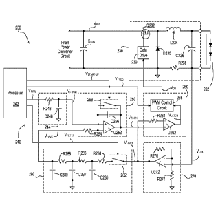
threshold kEARN-MAX
and the minimum learning threshold LEARN-MIN may be functions of a rated (or
maximum)
current 'RATED of the LED light source 202, for example, 0.0020 'RATED and
0.0002 ''RATED,
respectively. The processor 242 may be configured to periodically sample the
load voltage feedback
CA 03076810 2020-03-23
WO 2019/059962 PCT/US2018/019519
- 20 -
signal during the measurement window, and to process the plurality of samples
to determine the
learned load voltage VLEARNED. For example, the processor 242 may be
configured to process the
plurality of samples of the load voltage feedback signal by calculating an
average or median value of
the plurality of samples or filtering the samples using a digital low-pass
filter.
[0052] The processor 242 may be configured to measure the load voltage
VLoAD and
determine the learned load voltage VLEARNED when (e.g., each time that) the
processor 242 turns the
LED light source 202 off (e.g., fades the LED light source off). The processor
242 may be
configured to overwrite the learned load voltage VLEARNED stored in the memory
with the learned
load voltage VLEARNED determined the last time that the processor 242 turned
off the LED light
source 202. In addition, the processor 242 may be configured to process the
learned load
voltages VLEARNED from multiple turn-off events (e.g., calculate the average
or median value of the
multiple learned load voltages) before overwriting the learned load voltage
VLEARNED stored in the
memory.
[0053] The processor 242 may be configured to control the LED drive circuit
230 using the
learned load voltage VLEARNED, for example, when turning on the LED light
source 202. Fig 5B
shows example waveforms illustrating the operation of the LED driver 200 when
the processor 242
is fading on the LED light source 202 (e.g., fading on to a target intensity L
FRG]: that corresponds to
a target current I IRGT). In response to receiving a command to turn on the
LED light source 202
and/or in response to power being applied to the LED driver 200 to turn on the
LED light source, the
processor 242 may be configured to pre-charge the output capacitor C236 of the
LED drive
circuit 230 during a pre-charge period TPRE-CHARGE prior to attempting to turn
on the LED light
source 202. During the pre-charge period TPRE-CHARGE, the processor 242 may be
configured to
control the duty cycle of the pulse-width modulated signal Vpwm (and thus the
DC magnitude of the
target-current control signal VI-TRGT) as a function of the learned load
voltage VLEARNED to cause the
output capacitor C236 to charge faster than normal (e.g., faster than if the
processor 242 controlled
the DC magnitude of the target-current control signal VI-TRGT in response to
the target current 'TROT
as shown in Fig. 3B). The faster rate at which the output capacitor C236
charges during the
CA 03076810 2020-03-23
WO 2019/059962 PCT/1JS2018/019519
-21 -
pre-charge period TPRE-CHARGE may allow the processor 242 to turn-on the LED
light source 202
quickly and consistently, e.g., when fading the LED light source on to the low-
end intensity LLE.
[00541 The control circuit 240 may be configured to pre-charge the output
capacitor C236 of
the LED drive circuit 230 until the magnitude of the load voltage VLoAD
reaches or exceeds a
pre-charge voltage threshold Vi-pc. The pre-charge voltage threshold VTH-PC
may be determined,
for example, as a function of the learned load voltage VLEARNED (e.g, VTH-pc =
a = VLEARNED, where
a is a constant that may be, for example, approximately 0.90). Since the
magnitude of the load
voltage VLoAD may be greater when the LED light source 202 is cold than when
the LED light
source 202 is warm, the constant a may be sized to be less than one to ensure
that the LED drive
circuit 230 does not overshoot the learned load voltage VLEARNED when pre-
charging the output
capacitor C236. Additionally or alternatively, the pre-charge voltage
threshold VTH-PC may be
determined, for example, using a different function of the learned load
voltage VLEARNED (e.g.,
VTH-PC = VLEARNED - 13, where 13 is a constant that may be, for example,
approximately one volt).
Additionally or alternatively, the pre-charge voltage threshold VTH-Pc may be
a fixed threshold (e.g.,
a predetermined threshold). The processor 242 may be configured to cease pre-
charging the output
capacitor C236 if the magnitude of the load voltage VLoAD does not exceed the
pre-charge voltage
threshold VTH-pc within a timeout period. The processor 242 may be configured
to select the value
of the duty cycle of the pulse-width modulated signal Vpwm based on the
learned load
voltage VLEARNED such that pre-charge period TPRE-CHARGE for the LED driver
200 may be
approximately the same for different LED light sources that have different
resulting load voltages.
[00551 The processor 242 may control the start-up control signal VSTART-UP
to render the
controllable switching circuit 258 of the integrator circuit 250 conductive
during the pre-charge
period TPRE-CHARGE. After the magnitude of the load voltage VLOAD reaches or
exceeds the
pre-charge voltage threshold Vi-pc, the processor 242 may control the start-up
control
signal VSTART-UP to render the controllable switching circuit 258 of the
integrator circuit 250
non-conductive. This may allow the integrator circuit 250 and the latch
circuit 260 to control the
LED drive circuit 230 using closed loop control in response to the current
feedback signal Vi-FH to
regulate the magnitude of the load current koAD towards the target current
ITRGT.
CA 03076810 2020-03-23
WO 2019/059962 PCT/US2018/019519
- 22 -
[0056] Fig. 6 is a simplified flowchart of an example control procedure 600
for controlling a
load control device (e.g., the LED driver 200) to control a magnitude of a
load current conducted
through a lighting load (e.g., the LED light source 202). The control
procedure 600 may be executed
by a control circuit of the load control device (e.g., the control circuit 240
of the LED driver 200) at
step 610, for example, periodically and/or in response to a change in the
target current ITRGT for the
lighting load. If the target current 'TROT is less than the transition current
ITRAN at 612 (e.g, when the
target intensity LmoT in near the low-end intensity LLE), the control circuit
may maintain the
magnitude of the target-current control signal VI-TRGT constant (e.g., at the
minimum voltage VimiN)
at 614, and may adjust the frequency of the frequency control signal VFREQ in
response to the target
current ITRGT (e.g., as shown in Fig. 3A) at 616. The control circuit may then
control a filter circuit
(e.g., the filter circuit 280) at 618 by controlling the filter control signal
VFILTER to be periodic (e.g.,
having the same frequency of the frequency control signal VFREQ) and
synchronized to the frequency
control signal VFREQ (e.g., as shown in Fig. 4A). The control procedure 600
may then exit.
[0057] If the target current ITRGT is greater than the transition current
ITRAN (e.g., greater than
or equal to the transition current IrRAN) at 612 (e.g., when the target
intensity LIRG I' in near the
high-end intensity LHE), the control circuit may maintain the frequency of the
frequency control
signal \TFREo constant (e.g., at the maximum operating frequency fmAx) at 620,
and may adjust the
magnitude of the target-current control signal VI-TRGT in response to the
target current ITRGT (e.g., as
shown in Fig. 3B) at 622. The control circuit may then control the filter
control signal VFILTER to be
substantially constant at 624, before the control procedure 600 exits. For
example, the control circuit
may drive the control signal VFILTER using a maximum duty cycle, such as 100%
(e.g., by constantly
driving the filter control signal VFILTER high as shown in Fig. 4B), or a
substantially high duty cycle
(e.g., 90% or greater) at 624.