Note: Descriptions are shown in the official language in which they were submitted.
LARGE FAN-IN RQL GATES
RELATED APPLICATIONS
[0001] This application claims priority from U.S. Patent Application
Serial
No. 15/810907, filed 13 November 2017, which issued as U.S. Patent No.
10,171,087.
TECHNICAL FIELD
[0002] The present invention relates generally to quantum and classical
digital
superconducting circuits, and specifically to large fan-in reciprocal quantum
logic (RQL) gates.
BACKGROUND
[0003] In the field of digital logic, extensive use is made of well known
and highly
developed complimentary metal-oxide semiconductor (CMOS) technology. As CMOS
has
begun to approach maturity as a technology, there is an interest in
alternatives that may lead to
higher performance in terms of speed, power dissipation computational density,
interconnect
bandwidth, and the like. An alternative to CMOS technology comprises
superconductor based
single flux quantum circuitry, utilizing superconducting Josephson junctions
(lls), with typical
signal power of around 4 nanowatts (nW), at a typical data rate of 20 gigabits
per second (Gb/s)
or greater, and operating temperatures of around 4 kelvins.
[0004] "Fan-in" describes the number of inputs a logic gate can handle.
The larger the
fan-in, the more inputs can be handled by the gate. Logic gates with higher
fan-in can be
employed in digital logic design to reduce the depth of a logic circuit,
improving circuit
efficiency and density. A majority gate is a logical gate that returns true if
and only if more than
50% of its inputs are true.
SUMMARY
[0005] One example includes a reciprocal quantum logic (RQL) gate
circuit. The RQL
gate circuit has an input stage having more than two logical inputs each
configured to be asserted
based on receiving a positive single flux quantum (SFQ) pulse. The input stage
has, for each
1
Date Recue/Date Received 2021-09-09
CA 03077090 2020-03-25
WO 2019/094160 PCT/US2018/056305
logical input, at least one storage loop associated with the logical input.
Each storage loop
includes at one input Josephson junction (JJ), at least one inductor, and a
logical decision JJ. The
logical decision JJ is common to all the storage loops associated with the
logical inputs. The
RQL gate further has an output stage configured to assert an output based on a
triggering of the
logical decision JJ in response to a combination of logical inputs. It can
also de-assert an output
based on an untriggering of the logical decision JJ in response to a different
combination of
logical inputs.
[0006] Another example includes a method of determining a logic value,
based on logical
inputs. One or more positive SFQ pulses are provided to assert one or more
logical inputs of an
RQL gate having more than two logical inputs. One or more positive currents
are thereby placed
in one or more input storage loops in the RQL gate, which has at least one
storage loop per
logical input. A logical decision JJ in the RQL gate is thereby triggered in
response to a
combination of logical inputs. An assertion signal is thereby propagated from
an output of the
RQL gate.
[0007] Another example includes a circuit having more than two logical
input Josephson
transmission lines (JTLs) that intersect at a dovetail node. Each logical
input JTL includes a
storage loop input inductor connected, at a first node, to an input JJ and a
storage inductor. The
storage loop input inductor, input JJ, and storage inductor are sized with
respect to one another to
provide unidirectional data flow. A logical decision JJ is connected between
the dovetail node
and a low-voltage node, such that respective storage loops are formed by the
input JJ and storage
inductor of each input JTL and the logical decision JJ. An output JTL between
the dovetail node
and a logical output node provides an asserted or de-asserted logical output
signal at the output
node based on asserted or de-asserted logical input signals provided to the
logical input JTLs.
BRIEF DESCRIPTION OF THE DRAWINGS
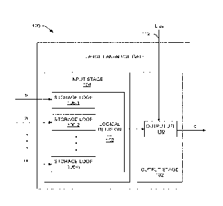
[0008] FIG. 1 is a block diagram of an example large fan-in reciprocal
quantum logic
(RQL) gate.
[0009] FIG. 2 is a circuit diagram of an example 3-of-5 majority gate.
2
CA 03077090 2020-03-25
WO 2019/094160 PCT/US2018/056305
[0010] FIGS. 3A and 3B illustrate an example single-input assertion
sequence in the gate
of FIG. 2.
[0011] FIGS. 4A-4C illustrate an example majority input assertion sequence
in the gate
of FIG. 2.
[0012] FIG. 5 is a circuit diagram of an example 3-of-5 majority gate.
[0013] FIG. 6 is a circuit diagram of an example AND gate.
[0014] FIG. 7 is a circuit diagram of an example OR gate.
[0015] FIG. 8 is a circuit diagram of an example OA gate.
[0016] FIG. 9 is a flow diagram of an example method of determining a
logical OR value
based on SFQ pulse inputs.
[0017] FIG. 10 is a flow diagram of an example method of determining a
logical AND
value based on SFQ pulse inputs.
[0018] FIG. 11 is a flow diagram of an example method of determining a
logical OR
value based on SFQ pulse inputs.
[0019] FIG. 12 is a flow diagram of an example method of determining a
logical OA
value based on SFQ pulse inputs.
[0020] FIGS. 13A and 13B are flow diagrams of example methods of
determining a
logical output from an RQL gate having more than two inputs based on SFQ pulse
inputs.
DETAILED DESCRIPTION
[00211 This disclosure relates generally to logical gate circuits for use
in reciprocal
quantum logic (RQL) systems and related methods. This disclosure more
specifically relates to
such gates having more than two inputs (in some examples many more than two),
including
majority gates, AND gates, OR gates, and OR-AND (OA) gates.
[0022] FIG. 1 shows large fan-in RQL gate 100 having a number, greater than
two, of
logical inputs li through ni, and output o. Gate 100 includes output stage
102, configured to
provide output o, and input stage 104. configured to receive inputs li through
ni, which can
consist of positive or negative single flux quantum (SFQ) pulses corresponding
to asserted or de-
3
CA 03077090 2020-03-25
WO 2019/094160 PCT/US2018/056305
asserted logic states, respectively. Each input has associated with it at
least one storage loop
among storage loops 106-1 through 106-n. Although input stage 104 is
illustrated as having one
storage loop per input, each input can have more than one storage loop
associated with it.
Logical decision Josephson junction (JJ) 108 is common to (i.e., shared by)
all logical input
storage loops, and triggers based on inputs Ii through ni. The assertion or de-
assertion of output
o is based on the triggering of logical decision JJ 108. For example, output o
can propagate a
positive SFQ pulse corresponding to an asserted output logic state and a
negative SFQ pulse
corresponding to a de-asserted output logic state. Output stage 102 can
include an output
Josephson transmission line (JTL) to amplify the output of logical decision JJ
108.
[0023] The triggering of logical decision JJ 108 can be based not only on
inputs li
through ni, but also on a bias signal 112 provided to output stage 102, e.g.,
to output JTL 110.
Bias signal 112 can provide both AC and DC bias. Thus, for example, bias
signal 112 can act as
a clock to RQL gate 100, causing the evaluation of the inputs li through ni to
produce the
output o at certain points in time according to the AC component of bias
signal 112.
[0024] FIG. 2 illustrates an RQL gate that can have a number of
configurations to
provide a number of different logical functions. Specifically, the illustrated
configuration 200
provides a 3-of-5 majority gate having an output Josephson transmission line
(JTL) stage 202 to
provide amplification and an input stage 204 having a number of JTL input
branches that join at
dovetail node 206. Together with logical decision JJ b3_0, the input branches
form storage loops
to receive and store inputs until a logical decision can be made, i.e., until
a logic condition is
met. Output JTL stage 202 includes JJs b0_0 and bl_O along with inductor
FL3_0. L4_0, and
L5_0 and an AC and DC bias bias_0. In input stage 204, a separate input
storage loop is
associated with each input. The input storage loop for input ai includes JJs
b2a_0 and b3_0, as
well as inductor FLstora_0. Leading inductor FL6a_0 allows input alto be
connected to a
driving JTL or to the output of another gate.
100251 The selections of component sizes in this storage loop provide a
unidirectional
data flow. Circuit 200 operates on SFQ pulses, which each place one (100
(about 2.07 mA pH) of
current into a storage loop. The magnitude of current through such a storage
loop is determined
4
CA 03077090 2020-03-25
WO 2019/094160 PCT/US2018/056305
by the size of the storage inductor in the storage loop. Thus, for each input,
the inductance value
of the storage loop input inductor (e.g., FL6a_0) can be small (e.g.. between
about 8 pH
and 9 pH, e.g., 8.5 pH) in comparison to the inductance value of the storage
inductor (e.g.,
FLstora_0). On the other hand, the storage inductor can size to be relatively
large (e.g., between
about 30 pH and 40 pH, e.g., 35 pH) (e.g., about four times larger than the
corresponding storage
loop input inductor) to reduce the magnitude of the stored current induced by
an input SFQ
pulse. In some examples, the magnitude of a current introduced at an input
(e.g., ai) is about
four times larger than the current stored in a storage loop. The input JJ for
input ai, b2a_0, is
also sized such that the driving JTL is capable of flipping this JJ to put
current into the storage
loop, but the current in the storage loop is never sufficient to unflip input
JJ b2a_0 and allow the
stored pulse to back out of the input.
10026] The storage loops associated with inputs bi, ci, di, and ei can have
the same
structure as the storage loop for input ai, all overlapping at logical
decision JJ b3_0. Output mo
may also be connected to a JTL or to the input of another gate, for example,
to propagate a
positive output pulse representing the assertion of gate 200 to logical
"high." A subsequent
negative output pulse propagated from output mo can then represent the de-
assertion of gate 200
to logical "low."
[0027] Logical decision JJ b3_0 performs the logic function of the gate
200. The
combination of any three inputs, plus the bias bias_0, is sufficient to switch
logical decision JJ
b3._0 in either direction. In circuit 200, no bias is applied directly to
logical decision JJ b3_0, but
a small amount may reach logical decision JJ b3_0 from both the bias of the
output JTL and from
the input JTLs. As mentioned with respect to bias signal 112 in gate 100 of
FIG. 1, an AC
component (e.g., a sine wave component) of bias signal bias_O in gate 200 of
FIG. 2 can act as a
clock signal to gate 200, which can evaluate the logical inputs twice per
cycle of the clock signal.
The AC phase of bias signal bias_O can have alternating positive and negative
portions. During
the positive portion of the AC phase, gate 200 evaluates inputs ai through ei
to decide whether
output mo should be asserted; during the negative portion of the AC phase,
gate 200 evaluates
inputs ai through ei to decide whether output mo should be de-asserted.
CA 03077090 2020-03-25
WO 2019/094160 PCT/US2018/056305
[00281 FIGS. 3A and 3B illustrate the sequence of events in gate circuit
200 when a
single input is asserted. In FIG. 3A, an input pulse, e.g., a single flux
quantum (SFQ) pulse,
arrives at input ai. This induces superconducting current 302 through leading
inductor FL6a_0
and input JJ b2a_0. Current 302 in turn triggers input JJ b2a_0, raising its
superconducting
phase to 27r, as indicated by the dot above input JJ b2a_0 in FIG. 3B. As
shown in FIG. 3B, the
triggering of input JJ b2a_0 induces an equal and opposite current (e.g., one
(Do worth of current)
in leading inductor FL6a_0, annihilating 304 the initial input current, and
also induces
superconducting current 306 in the loop formed by input JJ b2a_0, input loop
storage inductor
FLstora_0, and logical decision JJ b3_0. Current 306 alone is insufficient to
trigger logical
decision JJ b3_0, and will remain trapped indefinitely if no further inputs
are applied. A
negative input pulse arriving at input ai would reverse the above-described
effects, annihilating
current 306 and returning the circuit to its initial state. Inputs bi, ci, di,
and ei operate in exactly
the same manner, as they are perfectly symmetrical with input ai.
100291 Current 306 alone is insufficient to trigger logical decision JJ
b3_0, even with the
AC and DC bias bias_0, not only because b3_0 may be a larger JJ than the Jjs
preceding it in
circuit 200, but also because of the majority structure of circuit 200. The
additional load
presented to logical decision JJ b3_0 by the components associated with
unasserted inputs bi
through ei inhibits logical decision JJ b3_0 from triggering. Thus, assertion
of a majority of
inputs are required to cause b3_0 to trigger.
[00301 FIGS. 4A-4C illustrate the sequence of events in gate circuit 200
when a majority
of the inputs are asserted. FIG. 4A shows the state of circuit 200 after three
inputs, i.e., a
majority of the five inputs ai through ei, have been asserted. In the
illustrated example, inputs ai,
ci, and ei have been asserted. Just as in FIG. 3B. current 306, associated
with input ai, circulates
in the storage loop formed by input JJ b2a_0, input loop storage inductor
FLstora_0, and logical
decision JJ b3_0. Additionally, currents 402 and 404, associated with inputs
ci and ci,
respectively, circulate in the respective loops formed by input JJ b2c_0,
input loop storage
inductor FLstorc_0, and logical decision JJ b3_0 for input ci, and input LI
b2e_0, input loop
storage inductor FLstore_0, and logical decision JJ b3_0 for input ei. As
indicated by dots above
6
CA 03077090 2020-03-25
WO 2019/094160
PCT/US2018/056305
them, all three input JJs b2a_0, b2c_0, and b2e_0 are in the 2x state. A loop
current like 306,
402, or 404, induced by a positive input pulse, will persist in its storage
loop until a subsequent
negative pulse on the respective input removes it, or until the clocking
function of the AC
component of bias signal bias_O triggers logical decision JJ b3_0 to transform
the inputs into an
output. Because of this storage functionality, inputs needed to amount to a
majority number of
input assertions need not arrive within the same clock cycle.
[0031] All
three of the input loop currents 306, 402, 404 bias logical decision JJ b3_0
towards a positive transition, but due to the size of input loop storage
inductors FLstora_0,
FLstorc_0, and FLstore_0, currents 306, 402, 404 are insufficient to cause
this transition without
additional bias current provided by the AC and DC bias bias_0. When the AC
bias has reached
sufficient positive magnitude, i.e., when gate 200 is positively "clocked,"
logical decision JJ
b3_0 triggers, as indicated by the dot above it in FIG. 4B, which shows the
result of this
transition. The stored currents in input loop storage inductors FLstora_0,
FLstorc_0, and
FLstore_O are annihilated 406, 408, 410. New currents 412, 414 are induced in
the storage loops
associated with inputs hi and di, but in the opposite direction. Additionally,
current 416 is driven
through inductor FL3_0 and JJ b0_0. This current, in combination with the AC
bias, will trigger
amplifying JJ b0_0 as shown in FIG. 4C. This triggering of amplifying JJ b0_0
will
annihilate 418 the current in inductor FL3_0 and induce current 420 through
inductors L4_0
and L5_0 and output JJ bl_0. Although not shown in FIG. 4C, current 420 will
then trigger
output JJ bl_.0, propagating an output signal to the output mo of gate 200.
Since all inputs are
symmetric, this same series of events can happen with any combination of three
or more asserted
inputs to drive the output mo of gate 200 logical "high," giving the correct
logical function for
asserting the output of a 3-of-5 majority gate.
[0032] The
induced current 412 in the bi input storage loop formed by input JJ b2b_0,
input loop storage inductor FLstorb_0, and logical decision JJ b3_0, as well
as the induced
current 414 in the di input storage loop formed by input JJ b2d_0, input loop
storage inductor
FLstord_0, and logical decision JJ b3_0, biases logical decision JJ b3_0
towards a negative
transition, but not sufficiently to cause the transition alone, even with the
AC and DC bias
7
CA 03077090 2020-03-25
WO 2019/094160 PCT/US2018/056305
bias_0. This puts circuit 200 in the correct state to perform the correct
logical function for de-
asserting the 3-of-5 majority gate. A single negative pulse arriving at any of
the initially asserted
inputs ai, ci, or ei will provide negatively biasing currents in three storage
loops, such that in
combination with the AC and DC bias they will unflip logical decision JJ b3_0
by causing it to
transition out of its 27t phase, thereby de-asserting the output mo of gate
200 back to logical
"low." This will occur when the AC bias has reached sufficient negative
magnitude, i.e., on the
negative portion of the AC bias component of bias signal bias_0. If, instead,
a fourth positive
input were to arrive on either of inputs bi or di, it would annihilate the
respective stored negative
current 412 or 414 and negative input pulses would be required at any two of
the asserted inputs
before de-asserting the output mo, again providing the correct function for a
3-of-5 majority gate.
[0033] As another example implementation, FIG. 5 shows gate 500 which is
more similar
to the 2-of-3 majority topology. The example of gate 500 eliminates JJ b3_0
and inductor FL3_0
of the previously described example gate 200. JJ b0_0 has been increased in
size to about the
sum of the b3_0 and b0_0 in gate 200. In example circuit 500, b0_0 serves as
both the logical
decision JJ and the first JJ of the output JTL stage of gate 500.
[0034] The illustrated topologies 200, 500 can be extended to larger
majority gates,
e.g., a 4-of-7 majority gate, a 5-of-9 majority gate, etc. Provided that the
number of inputs is
odd, the basic topologies 200, 500 can extend to an arbitrary number of
inputs. However, as the
number of inputs is increased, the operating margins decrease.
100351 Gates 200 or 500 can also serve as the basis of several three-input
logic gates.
Grounding two of the inputs (effectively tying them to logical "low") creates
a three-input AND
gate with the remaining three inputs. Using a DC bias to induce one Coo (i.e.,
one SFQ pulse) of
current on two of the inputs (effectively tying them to logical "high")
creates a three-input OR
gate from the remaining inputs. In both cases, these derivative gates can be
optimized by
removing the input JJ on the inputs that are held at a constant logical state
and combining the
inductors of these two inputs in parallel.
[0036] Following from the above description, FIG. 6 shows example AND gate
aX), in
which output ao is asserted if and only if all three of inputs ai, bi, and ci
are asserted. In the
8
CA 03077090 2020-03-25
WO 2019/094160 PCT/US2018/056305
illustrated configuration, substitute storage inductor FLstord_O can be
approximately half the
size of FLstora_0, FLstorb_0, or FLstorc_0, in terms of its inductance value,
because it
substitutes for two storage inductors in parallel. Substitute storage inductor
FLstord_O may be
somewhat larger than half the size of any of the other storage inductors to
compensate for the
eliminated parasitic input inductance of the input JJs b2d_0 and b2e_0 from
the previous
example gates 200, 500. For example, in gate 600, the inductance value of
substitute storage
inductor FLstord_O can be between about 16 pH and 21 pH, e.g., 18 pH.
100371 In AND gate 600 of FIG. 6, once logical decision JJ b3_0 triggers
in response to
asserted inputs ai, bi, and ci, positive currents in storage inductors
FLstora_0, FLstorb_0, and
FLstorc_0 are destroyed, a negative current is induced into substitute storage
inductor FLstord_0,
and a positive current is propagated along the output JTL stage and out of
output ao. Thereafter,
if any negative pulses are applied to de-assert any of logical inputs ai, bi,
or ci, one or more
negative currents stored in any of the storage loops associated with the
logical inputs combines
with the negative current stored in substitute storage inductor FLstord_O to
bias logical decision
JJ b3_0 to untrigger upon the next negative portion of the AC component of the
bias signal
bias 0, which in turn propagates a negative pulse out of output ao.
100381 FIG. 7 shows example three-input OR gate 700, which is modified
from the
example majority gate 200 in a similar fashion to the three-input AND gate 600
of FIG. 6, but
introduces an additional JJ, bias quantizing JJ b2d_0, between transformer-
coupled input
inductor DC_d_O and substitute storage inductor FLstord._0. In OR gate 700,
output oo is
asserted if any one or more of the three inputs ai, bi, and ci is asserted. As
in circuit 600,
substitute storage inductor FLstord_O is about half the size, or somewhat
larger than half the size,
of storage inductors FLstora_0, FLstorb_0, and FLstorc_0. Transformer-coupled
input
inductor DC_d_O is transformer-coupled to DC flux bias line 702. Bias
quantizing JJ b2d_0
quantizes the DC bias current supplied through DC bias DC_d_O and improves
operating
margins. Bias quantizing JJ b2d_0 may be quite large, e.g., about twice the
size of any of input
JJs b2a_0, b2b_0, or b2c_0.
9
CA 03077090 2020-03-25
WO 2019/094160 PCT/US2018/056305
[00391 DC current provided through DC flux bias line 702 stays constant
throughout
system operation. At system start-up, the DC current through DC flux bias line
702 couples
current into input inductor DC_d_O to which it is transformer-coupled, via the
AC transient that
occurs at system power-up. This triggers bias quantizing JJ b2d_0 once at the
beginning of
operation, putting a positive current into substitute storage inductor
FLstord_0, which, because
of the component sizings, counts double toward the biasing of logical decision
JJ b3_0 as
compared to biasing from any of the logical inputs ai, bi, or ci.
[0040] Logical decision JJ b3_0 in OR gate 700 of FIG. 7 then effectively
sees "two" out
of "five" inputs asserted, the "two" asserted inputs being the non-logical,
phantom "inputs"
initiated by the DC bias, and triggers in response to at least one asserted
input among logical
inputs ai, bi, and ci. Upon such triggering, the positive current in
substitute storage inductor
FLstord_0 is destroyed, b2d_0 does not untrigger. positive currents in storage
inductors
FLstora_0, FLstorb_0, or FLstorc_O are destroyed should the inputs associated
with those
storage inductors have been asserted, negative currents are induced in the
storage inductors
associated with any unasserted inputs, and a positive current is propagated
along the output JTL
stage and out of output oo.
[0041] Thereafter, if negative pulses are applied to de-assert all of
previously asserted
inputs among logical inputs ai, bi, or ci, the negative currents stored in the
storage loops
associated with the logical inputs combine to bias logical decision JJ b3_0 to
untrigger upon the
next negative portion of the AC component of the bias signal bias_0, which in
turn propagates a
negative pulse out of output oo. This untriggering of logical decision JJ
b3...0 restores the
positive current to substitute storage inductor FLstord_0, bringing the
circuit back to its initial
state, i.e., the state following start-up injection of initial positive
current into substitute storage
inductor FLstord_0 via DC flux bias line 702.
[00412] FIG. 8 shows an example OR-AND (OA) gate, and more specifically a
three-
input 021 gate 800, constructed based on the previously described topologies.
Conceptually,
an OA gate is an AND gate having at least one of its inputs provided by the
output of an OR
gate. An OA gate thus provides an asserted output only when all of the inputs
to its conceptual
CA 03077090 2020-03-25
WO 2019/094160 PCT/US2018/056305
AND stage are asserted, in turn requiring that that at least one of the inputs
to its at least one
conceptual OR stage is asserted. An 0A21 gate is an OA gate having two inputs
to its
conceptual OR stage and, in addition to the output of its conceptual OR stage,
one other input to
its conceptual AND stage. Thus, an 0A21 gate provides an asserted output only
when a first
logical input is asserted and at least one of the remaining two logical inputs
is asserted.
[0043] The function of 0A21 gate 800 in FIG. 8 is described by the Boolean
equation
oao = ai AND (bi OR ci). To accomplish this function, input ai can be placed
into two storage
loops that branch from single input ai, whereas bi and ci are each connected
to one storage loop.
In similar fashion to the input elimination illustrated by the previous
example gate 600 shown in
FIG. 6, an eliminated fifth input is replaced by substitute storage inductor
FLstore_0. In
gate 800, however, substitute storage inductor FLstore_O can be about the same
size as the other
storage inductors FLstora_0, FLstorb_0, FLstorc_0, and FLstord_0, as opposed
to being half the
size, as substitute storage inductor FLstord_O is in AND gate 600 in FIG. 6.
[0044] Connecting input ai directly to storage inductors FL6a_0 and FL6d_0
could
present too large a load for a single driving JTL of normal size to handle, so
input ai includes
additional JTLs, connected to bias signal lines bias_1_p0 and bias_2_p0,
respectively, to provide
the required amplification. As examples, in gate 800 of FIG. 8, storage loop
input
inductors FL6a_0 and FL6d_0 can have inductance values between about 8 pH and
9 pH
(e.g., 8.5 pH), JTL input inductors FL3_1 and FL3_2 can have inductance values
of between
about 20 pH and 21 pH (e.g., 20.5 pH), the values of inductors L4_1 plus L5_1,
as well as L4_2
plus L5_2, can be chosen to sum to between about 14 pH and 15 pH (e.g., 14.5
pH), and bias
inductors L2_1 and L2_2 can be sized to be slightly smaller than they would be
in a standard
JTL to provide extra power to J.Is bl_l and b1_2, enabling them to drive the
heavy load of input
ai of gate 800. The bias signals provided on lines bias_l_p0 and bia.s_2_p0
can have the same
phase as the bias signal from line bias_), but this is not strictly necessary
for the circuit to
function. In an example similar to gate 800 that is not illustrated, the two
paths attached to input
ai in parallel may be combined by doubling all the JJ sizes and halving all
the inductor sizes.
11
CA 03077090 2020-03-25
WO 2019/094160 PCT/US2018/056305
[0045] FIG. 9 illustrates an example method 900 of determining a logical
majority value
based on SFQ pulse inputs. Positive SFQ pulses are provided 902 to assert a
majority of the
logical inputs of an RQL majority gate to place 904 currents in a majority of
input storage loops.
The RQL majority gate can be, for example, like gates 200 or 500 shown in
FIGS. 2 and 5, or
can be extensions of such examples that provide a greater odd number of
inputs, as described
above. Thus, for example, the RQL majority gate used in the method may
comprise no more
than eight JJs and no more than fourteen inductors, as shown in FIG. 2. For
example, the RQL
majority gate used in the method may comprise no more than seven JJs and no
more than
thirteen inductors, as shown in FIG. 5. A JJ that is configured to trigger
only when a majority of
the logical inputs are asserted then triggers 906. The JJ can be so
configured, for example, by
making it common to a plurality (e.g., all) of the input storage loops, by
providing appropriate
biasing, and/or by appropriate component sizing. An assertion signal,
generated as a result of the
triggering, then propagates 908 from an output of the RQL majority gate. The
assertion signal
can be, for example, a single SFQ pulse.
[0046] FIG. 10 illustrates an example method 1000 of determining a logical
AND value
based on more than two SFQ pulse inputs. Positive SFQ pulses are provided 1002
to assert all of
the logical inputs of an RQL AND gate having more than two logical inputs to
place 1004
currents in input storage loops associated with the asserted inputs, e.g., one
loop per input. The
RQL AND gate can be, for example, like gate 600 shown in FIG. 6, or can be
extensions of such
example providing a greater number of inputs. Thus, for example, the RQL AND
gate used in
the method may comprise no more than six JJs and no more than eleven
inductors, as shown in
FIG. 6. A JJ that is configured to trigger only when all of the logical inputs
are asserted then
triggers 1006. The JJ can be so configured, for example, by making it common
to all of the input
storage loops, by effectively tying to logical "low" additional inputs not
counted among the
logical inputs, by providing appropriate biasing, and/or by appropriate
component sizing. An
assertion signal, generated as a result of the triggering, then propagates
1008 from an output of
the RQL AND gate. The assertion signal can be, for example, a single SFQ
pulse.
12
CA 03077090 2020-03-25
WO 2019/094160
PCT/US2018/056305
[0047] FIG. 11
illustrates an example method 1100 of determining a logical OR value
based on more than two SFQ pulse inputs. Positive SFQ pulses are provided 1102
to assert any
or all of the logical inputs of an RQL OR gate having more than two logical
inputs to place 1104
currents in one or more input storage loops associated with the asserted
inputs, e.g., one loop per
input. The RQL OR gate can be, for example, like gate 700 shown in FIG. 7, or
can be
extensions of such example providing a greater number of inputs. A JJ that is
configured to
trigger when any of the logical inputs is asserted then triggers 1106. The JJ
can be so
configured, for example, by making it common to all of the input storage
loops, by effectively
tying to logical "high" additional inputs not counted among the logical
inputs, by providing
appropriate biasing, and/or by appropriate component sizing. An assertion
signal, generated as a
result of the triggering, then propagates 1108 from an output of the RQL OR
gate. The assertion
signal can be, for example, a single SFQ pulse.
[0048] FIG. 12
illustrates an example method 12(X) of determining a logical OA value
based on more than two SFQ pulse inputs. Positive SFQ pulses are provided 1202
to assert a
first of the logical inputs of an RQL OA gate having more than two logical
inputs, and also to
assert at least one of the remaining logical inputs of the RQL OA gate,
thereby placing 1204
currents in input storage loops associated with the asserted inputs, e.g., at
least one loop per
input. The RQL OA gate can be, for example, 0A21 gate 800 shown in FIG. 8, or
can be
extensions of such example providing a greater number of inputs, and/or
combining the two
branches of input ai as a single branch. The first of the logical inputs may
have two or more
input storage loops associated with it, or may have one storage loop built
with components
having values sized respectively to the components of the loops of the
remaining inputs. For
example, when the first of the logical inputs has two or more storage loops
associated with it, the
storage loops can be preceded by additional JTL stages to provide
amplification. In other
examples, when the first of the logical inputs has only one storage loop
associated with it, the JJs
of the one storage loop can be about double the value of the JJs in the
storage loops associated
with the remaining inputs, and the inductors of the one storage loop can be
about half the
inductance value of the us in the storage loops associated with the remaining
inputs. A JJ that is
13
CA 03077090 2020-03-25
WO 2019/094160 PCT/US2018/056305
configured to trigger when any of the logical inputs is asserted then triggers
1206. The JJ can be
so configured, for example. by making it common to all of the input storage
loops, by effectively
tying to logical "low" additional inputs not counted among the logical inputs,
by providing
appropriate biasing, and/or by appropriate component sizing. An assertion
signal, generated as a
result of the triggering, then propagates 1208 from an output of the RQL OA
gate. The assertion
signal can be, for example, a single SFQ pulse.
[0049] Methods 900, 1000, 1100, and 1200 are generalized as a method 1300
of
determining a logical output from an RQL gate having more than two logical
inputs based on
SFQ pulse inputs shown in FIG. 13A. Positive SFQ pulses are provided 1302 to
assert one or
more logical inputs of an RQL gate having more than two logical inputs to
place 1304 one or
more currents in one or more input storage loops associated with the asserted
inputs, e.g., one
loop per input, where the gate has more than two such storage loops. The RQL
gate can be, for
example, like any of gates 100, 200, 500, 600, 700, or 800, shown in FIGS. 1,
2, 5, 6, 7, or 8,
respectively, or can be extensions of such example providing a greater number
of inputs and/or
combining or splitting input storage loop branches. A JJ that is configured to
trigger based on
the assertion of a certain number or certain ones of the logical inputs then
triggers 1306. The JJ
can be so configured, for example, by making it common to all of the input
storage loops, by
effectively tying to logical "high" or logical "low" additional inputs not
counted among the
logical inputs, by providing appropriate biasing, and/or by appropriate
component sizing. An
assertion signal, generated as a result of the triggering, then propagates
1308 from an output of
the RQL gate. The assertion signal can be, for example, a single SFQ pulse.
[0050] FIG. 13B shows method 1350 of determining a logical output from an
RQL gate
having more than two logical inputs based on SFQ pulse inputs, which can
continue from
method 1.300 shown in FIG. 13A. Negative SR) pulses are provided 1310 to de-
assert one or
more logical inputs of an RQL gate having more than two logical inputs to
place 1312 one or
more currents in one or more input storage loops associated with the asserted
inputs, e.g., one
loop per input, where the gate has more than two such storage loops. The
placed currents can be
negative currents, i.e., currents equal and opposite to the currents placed
1304 in method 1300.
14
CA 03077090 2020-03-25
WO 2019/094160 PCT/US2018/056305
Again, the RQL gate can be, for example, like any of gates 100, 200, 500, 600,
700, or 800,
shown in FIGS. 1, 2, 5, 6, 7, or 8. respectively, or can be extensions of such
example providing a
greater number of inputs and/or combining or splitting input storage loop
branches. A JJ that is
configured to untrigger based on the de-assertion of a certain number or
certain ones of the
logical inputs then untriggers 1314. The JJ can be so configured, for example,
by making it
common to all of the input storage loops, by effectively tying to logical
"high" or logical "low"
additional inputs not counted among the logical inputs, by providing
appropriate biasing, and/or
by appropriate component sizing. A de-assertion signal, generated as a result
of the triggering,
then propagates 1316 from an output of the RQL gate. The assertion signal can
be, for example,
a single SFQ pulse, e.g., a single negative SFQ pulse, opposite in direction
to the pulse
propagated 1308 in method 1300.
[00511 The use of logic gates with more than two inputs, including the
examples
disclosed herein, can improve the efficiency and density of RQL logic. While
logic functions
having more than two inputs can be built from two-input gates, the large
number of such gates
required to construct three-or-more-input gates can impact efficiency. Gates
that can implement
larger logic functions allow reduced die sizes and, by extension, reduced cost
per die. The logic
gates described herein can operate according to RQL data encoding, where, for
example, it
would be impermissible for a logic gate to propagate two positive output
pulses in a row or two
negative output pulses in a row.
[0052] What have been described above are examples of the invention. It is,
of course,
not possible to describe every conceivable combination of components or
methodologies for
purposes of describing the invention, but one of ordinary skill in the art
will recognize that many
further combinations and permutations of the invention are possible.
Accordingly, the invention
is intended to embrace all such alterations, modifications, and variations
that fall within the
scope of this application, including the appended claims. Additionally, where
the disclosure or
claims recite "a," "an," "a first," or "another" element, or the equivalent
thereof, it should be
interpreted to include one or more than one such element, neither requiring
nor excluding two or
more such elements. As used herein, the term "includes" means includes but not
limited to, and
CA 03077090 2020-03-25
WO 2019/094160
PCT/US2018/056305
the term "including" means including but not limited to. The term "based on"
means based at
least in part on.
16