Note: Descriptions are shown in the official language in which they were submitted.
CA 03079049 2020-04-14
DESCRIPTION
POWER STORAGE DEVICE
Technical Field
[0001]
The present invention relates to a power storage device having a simple
structure in which a functional layer is integrated with an electrode.
Background Art
[0002]
Secondary batteries that are power storage devices include secondary
batteries and electrochemical capacitors that store electricity as
electrochemical
energy by using an oxidation-reduction reaction, capacitors that can store as
a
change in capacity of an electric double layer. Further, as the secondary
battery
is known not only an aqueous secondary battery such as a nickel hydride
secondary battery, but also a non-aqueous secondary battery such as a lithium
ion
secondary battery using an active material which is effective for an ion
insertion
reaction.
[0003]
Lithium ion secondary batteries are widely used mainly in electronic
devices such as portable devices. This is because the lithium ion secondary
batteries have a high voltage, have a large charging and discharging capacity,
etc.
[0004]
However, in recent years, polymer batteries that use gel type electrolytes
instead of electrolytic solutions and thin-film solid-state secondary
batteries that
use solid-state electrolytes have been developed so that portable devices,
etc. can
be configured to be thinner and smaller and further for safety.
[0005]
Patent Literatures 1 and 2 disclose all-solid secondary batteries using metal
oxide semiconductors.
[0006]
Patent Literature 3 describes a thin-film solid-state secondary battery
element in which a first electrode, an electron transport layer, a charging
layer, an
electron block layer, and a second electrode are sequentially laminated above
a
substrate. The charging layer contains an inorganic material. The electron
CA 03079049 2020-04-14
2
transport layer is made of an inorganic oxide material, and the inorganic
material
oxide contains niobium oxide or tungsten oxide.
[0007]
Patent Literature 4 discloses a power storage element having a structure in
which a conductive first electrode, a power storage layer (charging layer)
containing an insulating material and n-type semiconductor particles, a leak
suppression layer, a p-type semiconductor layer, and a second electrode are
sequentially laminated.
Citation List
Patent Literature
[0008]
Patent Literature 1: International Patent Publication No. W02012/046325
Patent Literature 2: International Patent Publication No. W02013/065093
Patent Literature 3: Japanese Unexamined Patent Application Publication
No. 2014-154505
Patent Literature 4: Japanese Unexamined Patent Application Publication
No. 2016-82125
Summary of Invention
Technical Problem
[0009]
Power storage devices configured by laminating a plurality of functional
layers have configurations described in Patent Literatures 1 to 4, for
example.
As the number of layers to be laminated increases, the number of manufacturing
steps also increases according to the number of layers to be laminated, which
causes an increase in cost. Therefore, it has been desired to reduce the
number
of layers to be laminated.
[0010]
The present invention has an object to provide a power storage device
structure in which the number of layers to be laminated is reduced as compared
with a conventional power storage device.
Solution to Problem
[0011]
In order to solve the above problem, a power storage device according to
the present invention includes a conductive electrode, an insulator and an n-
type
CA 03079049 2020-04-14
3
metal oxide semiconductor, and has a structure in which a charging layer for
storing charges, and an electrode layer formed of a material of an
electrochromic
element are sequentially laminated.
[0012]
Here, iridium oxide is desirable for the electrode layer to be formed from
the material of the electrochromic element. A resistance adjusting material
may
be added to the electrode layer formed of iridium oxide to reduce the
resistance.
The resistance adjusting material is at least one of metal elements of
magnesium,
aluminum, tungsten, cobalt and nickel. Further, fluorine may be doped as a
resistance adjusting material. The iridium oxide layer whose resistance has
been
reduced by the resistance adjusting material preferably has a resistivity of
2x10⁻⁵
Om or less and a thickness of 200 nm or more.
[0013]
According to a first aspect of the power storage device of the present
invention, a negative conductive electrode, a charging layer including an
insulator
and an n-type metal oxide semiconductor, and an iridium oxide layer formed of
iridium oxide are sequentially laminated. Further, the electrode layer is
configured by an iridium oxide layer formed of iridium oxide.
[0014]
According to a second aspect of the power storage device of the present
invention, negative conductive electrode, an electron transport layer, a
charging
layer including an insulator and an n-type metal oxide semiconductor, and an
iridium oxide layer formed of iridium oxide are sequentially laminated. In
contrast with the first embodiment, the electron transport layer is added
between
the negative conductive electrode and the charging layer to increase the
efficiency
of transporting the electrons stored in the charging layer.
[0015]
According to third aspect of the power storage device of the present
invention, a negative conductive electrode, a charging layer including an
insulator
and an n-type metal oxide semiconductor, a leak suppression layer, and an
iridium
oxide layer formed of iridium oxide are sequentially laminated. In contrast
with
the first aspect, the leak suppression layer is added between the charging
layer
and the iridium oxide layer formed of iridium oxide to suppress leakage of
electrons stored in the charging layer, whereby a voltage holding time after
power
CA 03079049 2020-04-14
4
storage can be increased.
[0016]
According to a fourth aspect of the power storage device of the present
invention, a negative conductive electrode, an electron transport layer, a
charging
.. layer including an insulator and an n-type metal oxide semiconductor, a
leak
suppression layer, and iridium oxide layer formed of iridium oxide are
sequentially laminated. In contrast with the first aspect, the electron
transport
layer is added between the negative conductive electrode and the charging
layer,
and further, the leak suppression layer is added between the charging layer
and
the iridium oxide layer formed of iridium oxide. Therefore, the efficiency of
transporting electrons to a negative electrode side is increased, and leakage
of
electrons stored in the charging layer to a positive electrode side is
suppressed.
[0017]
According to a fifth aspect of the power storage device of the present
invention, a negative conductive electrode, an electron transport layer that
transports electrons, a first charging layer that includes an insulator and a
first n-
type metal oxide semiconductor, and stores charges, a second charging layer
that
includes the insulator and a second n-type metal oxide semiconductor which is
a
material different from the first charging layer, and an iridium oxide layer
formed
of iridium oxide are sequentially laminated.
[0018]
In contrast with the third aspect, the fifth aspect is configured so that the
charging layer is doubled. In the third embodiment, even if the thickness of
the
charging layer is increased in order to increase the charging capacity, the
.. charging capacity does not necessarily increase with the increase of the
thickness.
Therefore, the material of the n-type metal oxide semiconductor is changed to
form the second charging layer, and the charging capacity is increased.
[0019]
In the power storage devices according to the first to fourth aspects of the
present invention and the first charging layer and the second charging layer
according to the fifth aspect, the insulator is composed of at least one of
silicon
dioxide, aluminum oxide, and magnesium oxide. The n-type metal oxide
semiconductor is composed of at least one of titanium oxide, tin oxide, and
zinc
oxide.
CA 03079049 2020-04-14
[0020]
In the fifth aspect, the n-type metal oxide semiconductor of the first
charging layer is composed of at least one of titanium oxide, tin oxide, and
zinc
oxide. The n-type metal oxide semiconductor of the second charging layer is
5 also composed of at least one of titanium oxide, tin oxide and zinc
oxide, but is
made of a material different from the n-type metal oxide semiconductor used
for
the first charging layer.
[0021]
In the power storage devices according to the second, fourth and fifth
aspects of the present invention, the electron transport layer includes at
least one
of niobium oxide, tungsten oxide, titanium oxide, tin oxide or titanium oxide.
[0022]
In the power storage devices according to the third and fourth aspects of the
present invention, the leak suppression layer is composed of at least one of
silicon
oxide, silicon nitride, magnesium oxide, and aluminum oxide.
[0023]
In the first to fifth aspects according to the above-described embodiments,
the lamination order may be reversed. In this case, an iridium oxide layer
formed of iridium oxide is formed above an insulative substrate (insulating
substrate). This is because the iridium oxide layer formed of iridium oxide
may
be easily formed in some cases.
[0024]
With respect to the first aspect, the iridium oxide layer formed of iridium
oxide, the charging layer including the insulator and the n-type metal oxide
semiconductor, and the negative conductive electrode are sequentially
laminated
above the insulating substrate.
[0025]
With respect to the second aspect, the iridium oxide layer formed of iridium
oxide, the charging layer including the insulator and the n-type metal oxide
semiconductor, the electron transport layer, and the negative conductive
electrode
are sequentially laminated above the insulating substrate.
[0026]
With respect to the third aspect, the iridium oxide layer formed of iridium
oxide, the leak suppression layer, the charging layer including the insulator
and
CA 03079049 2020-04-14
6
the n-type metal oxide semiconductor, and the negative conductive electrode
are
sequentially laminated above the insulating substrate.
[0027]
With respect to the fourth aspect, the iridium oxide layer formed of iridium
oxide, the leak suppression layer, the charging layer including the insulator
and
the n-type metal oxide semiconductor, and the electron transport layer, and
the
negative conductive electrode are sequentially laminated above the insulating
substrate.
[0028]
With respect to the fifth aspect, the iridium oxide layer formed of iridium
oxide, the second charging layer including the insulator and the second n-type
metal oxide semiconductor, the first charging layer including the insulator
and the
first n-type metal oxide semiconductor, the electron transport layer, and the
negative conductive electrode are sequentially laminated above the insulating
substrate.
Advantageous Effect of Invention
[0029]
According to the present invention, it is possible to provide a power storage
device structure in which the number of layers to be laminated is reduced as
compared with a conventional power storage device.
Brief Description of the Drawings
[0030]
Fig. 1 is a schematic cross-sectional structural view of a power storage
device according to a first embodiment of the present invention;
Fig. 2 is a schematic structural view showing a conventional power storage
device;
Fig. 3 is a schematic cross-sectional structural view of a conventional
power storage device according to a second embodiment and a power storage
device according to the present invention;
Fig. 4 is a schematic cross-sectional structural view of a conventional
power storage device according to a third embodiment and a power storage
device
according to the present invention;
Fig. 5 is a schematic cross-sectional structural view of a conventional
power storage device according to a fourth embodiment and a power storage
CA 03079049 2020-04-14
7
device according to the present invention;
Fig. 6 is a schematic cross-sectional structural view of a conventional
power storage device according to a fifth embodiment and a power storage
device
according to the present invention;
Fig. 7 is a schematic cross-sectional structural view of a power storage
device when the lamination order of the first embodiment is reversed;
Fig. 8 is a flowchart showing a method of manufacturing a power storage
device according to the fifth embodiment of the present invention;
Fig. 9 is a charge/discharge characteristic measurement system for
measuring charge/discharge characteristics of the power storage device; and
Fig. 10 is a diagram showing charge/discharge characteristics of the
conventional power storage device in the fourth embodiment of the present
invention and the power storage device according to the present invention.
Description of Embodiments
[0031]
Next, embodiments will be described with reference to the drawings. In
the drawings described below, the same or similar portions are denoted by the
same or similar reference signs. However, the drawings are schematic.
Therefore, specific thicknesses and dimensions should be determined in
consideration of the following description. In addition, it is needless to say
that
the drawings include portions having different dimensional relationships and
ratios among them.
[0032]
The embodiments described below exemplify devices and methods for
embodying the technical idea, but do not specify the material, shape,
structure,
arrangement, and the like of each component.
[0033]
The power storage device targeted by the present invention is a power
storage device in which a p-type metal oxide semiconductor is laminated on a
conductive positive electrode. The p-type metal oxide semiconductor layer has,
for example, a function of blocking and suppressing electron leakage from the
charging layer. The power storage devices disclosed in Patent Literatures 1 to
4
are cited as conventional power storage devices having this function.
[0034]
CA 03079049 2020-04-14
8
These power storage devices are configured so that a structure in which a
charging layer for storing charges and a plurality of functional layers for
improving the performance of the power storage device are laminated is
sandwiched between positive and negative conductive electrodes. From the
viewpoint of simplification of the manufacturing process and cost, it is
effective
means to reduce the number of layers to be laminated.
[0035]
Therefore, attention has been paid to nickel oxide (NiO) in a p-type oxide
semiconductor layer, and the following examination has been performed.
[0036]
Nickel oxide (NiO) has properties as a p-type semiconductor, and is also
used for electrochromic elements. The electrochromic element has a structure
in
which an electrochromic material layer and a dielectric layer are laminated
between a positive electrode and a negative electrode.
[0037]
In this solid-state electrochromic element, a DC voltage is applied between
the positive electrode and the negative electrode to develop color with an
oxidation-reduction reaction. At this time, there is a problem that a leakage
current that does not directly contribute to color development flows. In
Japanese
Unexamined Patent Application Publication No. S55-88028, a current blocking
layer is provided between the dielectric layer and the solid-state
electrochromic
material layer in order to prevent the leakage current.
[0038]
In the power storage device targeted by the present invention, the charging
layer is composed of titanium oxide (TiO2) and silicon dioxide (SiO2) as an
insulating material, and the charging ability is improved by a manufacturing
method using an ultraviolet treatment.
[0039]
Nickel oxide (NiO) is used for the dielectric layer in the solid-state
.. electrochromic element having the electron blocking layer. It is
considerable
that materials usable for the dielectric layer of the solid-state
electrochromic
element including the electron blocking layer can be applied to the power
storage
device targeted by the present invention.
[0040]
CA 03079049 2020-04-14
9
Therefore, attention has been paid to the material used for the dielectric
layer of the solid-state electrochromic element, and a low-resistance material
has
been studied. Specifically, in the power storage device targeted by the
present
invention, nickel oxide is used for a p-type metal oxide semiconductor layer
in
contact with an electrode, and the possibility that the p-type metal oxide
semiconductor layer and the positive electrode can be integrated with each
other
has been investigated by searching a low-resistance material from materials
used
for the dielectric layer in the solid-state electrochromic element.
[0041]
Therefore, attention has been paid to iridium oxide (Ir203) having a low
resistance from the materials used for the dielectric layer of the solid-state
electrochromic element. Iridium oxide (Ir203) is also used as a counter
electrode
of an electrochromic element because it is insoluble and chemically stable and
has
a coloring property. The dielectric layer of the solid-state electrochromic
element may be regarded as an electrode layer. The resistivity is 49x10-811m.
For this reason, if iridium oxide (Ir203) is used as a p-type metal oxide
semiconductor, a power storage device having an integrated simple
configuration
which is provided with a function of an electrode can be realized.
[0042]
Generally, the resistance of the electrode is low, and in the case of a metal
electrode, for example, the resistivity of silver is 1.59x10-811m, the
resistivity of
copper is 1.68x10-811m, and the resistivity of aluminum is 2.82x10-811m. The
resistivity of ITO (Indium Tin Oxide), which is widely known as a transparent
electrode, is about 1.5x10-60m.
[0043]
It is difficult to form a film of iridium oxide with a low resistance, and the
resistivity greatly depends on a manufacturing condition. Above all, strict
condition control is required to mass-produce low-resistance iridium oxide
films,
which causes increase of the cost. Therefore, it is practically sufficient if
the
resistivity level of ITO can be realized. For example, the level was 5.05x10-
611m
on a trial basis in consideration of a production condition under mass
production
that enables stable production.
[0044]
Even in the production condition under mass production, a resistance
CA 03079049 2020-04-14
adjusting material may be added in order to further reduce the resistivity of
iridium oxide (Ir203). The resistance adjusting material includes metal
elements
such as magnesium (Mg), aluminum (Al), tungsten (W), cobalt (Co), and nickel
(Ni). The metal has good conductivity, and the resistivity of magnesium is
5 4.42x10-811m, the resistivity of aluminum is 2.82x10-811m, the
resistivity of
tungsten is 5.29x10-811m, and the resistivity of cobalt is 5.81x10-80m, and
the
resistivity of nickel is 6.99x10-80m, so that the metal can be used as a
resistance
adjusting material for lowering the resistance.
[0045]
10 Furthermore, in order to lower the resistivity of iridium oxide (Ir203),
fluorine (F) atoms may be doped. The fluorine (F) atom is a kind of halogen
element, belongs to Group 17 and has seven outermost shell electrons. Since
oxygen is an element of Group 16, it has six outermost shell electrons.
Therefore, the number of electrons to be received by fluorine (F) is smaller,
and
when oxygen of iridium oxide (Ir203) is replaced by fluorine (F), the number
of
electrons increases as a whole, so that the carrier density increases.
Therefore,
by doping fluorine into iridium oxide (Ir203), the resistivity can be lowered.
[0046]
The resistivity of iridium oxide (Ir203) can be lowered to 2x10-511m or less
by adding a metal element as a resistance adjusting material and further
doping
fluorine (F). Therefore, iridium oxide (Ir203) can be treated as a material
having
both a p-type metal oxide semiconductor and an electrode. Note that the
dielectric layer made of iridium oxide is simply referred to as an iridium
oxide
layer below.
[0047]
Next, a structure of a power storage device to which iridium oxide (Ir203)
can be applied and an embodiment to which the structure of the power storage
device is applied will be described.
<First Embodiment>
[0048]
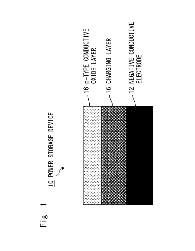
Fig. 1 shows a schematic cross-sectional structure showing a power storage
device 10 according to the present invention. The power storage device 10 has
a
structure in which a negative conductive electrode 12, a charging layer 14 for
storing charges, and an iridium oxide layer 16 are sequentially laminated.
CA 03079049 2020-04-14
11
[0049]
The power storage device 10 may be manufactured by sequentially
laminating the negative conductive electrode 12, the charging layer 14, and
the
iridium oxide layer 16 on an insulating substrate. For example, a glass
substrate
or a resin sheet of a polymer film can be used as the insulating substrate.
[0050]
The material of the negative conductive electrode 12 includes, for example,
a silver (Ag) alloy containing aluminum (Al). Examples of a method of forming
the negative conductive electrode 12 include a vapor deposition method such as
sputtering, ion plating, electron beam deposition, vacuum deposition, or
chemical
vapor deposition. Further, the negative conductive electrode 12 may be formed
by an electrolytic plating method, an electroless plating method, or the like.
As
a metal used for plating is generally usable copper (Cu), copper alloy, nickel
(Ni),
aluminum (Al), silver (Ag), gold (Au), zinc (Zn), tin (Sn), or the like.
[0051]
When the substrate is a conductive metal foil sheet, for example, a copper
foil sheet, an aluminum foil sheet or a stainless steel sheet, the substrate
can be
used as the negative conductive electrode 12.
[0052]
The charging layer 14 is a layer formed from an insulating material and an
n-type metal oxide semiconductor. The insulating material is, for example,
silicon dioxide (5i02) or a silicone oil having a siloxane bond. For example,
titanium oxide (TiO2), tin oxide (5n02), or zinc oxide (ZnO) is preferable as
the
n-type metal oxide semiconductor. Further, the n-type metal oxide
semiconductor may be a material obtained by combining any two elements of
(TiO2), tin oxide (5n02), or zinc oxide (Zn0), or a material obtained by
combining three elements of them.
[0053]
The specific structure of the charging layer 14 may be formed by a layered
structure of an insulating material and an n-type metal oxide semiconductor, a
structure in which the periphery of a particulate n-type metal oxide
semiconductor
is covered with an insulating material, or a structure in which a particulate
n-type
metal oxide semiconductor is buried and mixed in an insulating material.
[0054]
CA 03079049 2020-04-14
12
Titanium oxide (TiO2) is particularly desirable for the n-type metal oxide
semiconductor in order to perform modification based on a photoexcited
structural
change (photoinduced phase transition) by ultraviolet irradiation.
[0055]
The n-type metal oxide semiconductor used for the charging layer 14 is
generated by decomposition from a metal aliphatic acid salt in a manufacturing
process. For this reason, as the metal aliphatic acid salt are used those
which
can be decomposed or burned to be converted into metal oxides by irradiating
ultraviolet rays under an oxidizing atmosphere or baking. As the aliphatic
acid
are usable, for example, an aliphatic monocarboxylic acid or an aliphatic
polycarboxylic acid such as an aliphatic dicarboxylic acid, an aliphatic
tricarboxylic acid, or an aliphatic tetracarboxylic acid.
[0056]
More specifically, examples of saturated aliphatic monocarboxylic acid
include formic acid, acetic acid, propionic acid, caproic acid, enanthic acid,
caprylic acid, pelargonic acid, capric acid, and stearic acid. As unsaturated
aliphatic monocarboxylic acid are usable highly unsaturated monocarboxylic
acids
such as acrylic acid, butenoic acid, crotonic acid, isocrotonic acid,
linolenic acid,
and oleic acid.
[0057]
Since aliphatic acid salts are easily decomposed or burned by heating, have
high solvent solubility, form dense films after being decomposed or burned,
are
easy to handle and low in price, and easily synthesize salts with metals,
salts of
aliphatic acids and metals are preferable.
[0058]
Insulating resin as well as inorganic insulating material is usable as the
insulating material, and may include thermoplastic resin such as polyethylene,
polypropylene, polystyrene, polybutadiene, polyvinyl chloride, polymethyl
methacrylate, polyamide, polycarbonate, polyimide or cellulose acetate, or
thermosetting resin such as phenol resin, amino resin, unsaturated polyester
resin,
allyl resin, alkyd resin, epoxy resin or polyurethane.
[0059]
A method of forming the charging layer 14 is performed by spin coating.
First, for example, a solution is prepared by stirring fatty acid titanium and
CA 03079049 2020-04-14
13
silicone oil together with a solvent. This solution is coated onto the
negative
conductive electrode 12 using a spin coating device. The number of revolutions
is, for example, about 500 to 3000 rpm. After the coating, it is dried on a
hot
plate. The drying temperature on the hot plate is, for example, about 30 C to
200 C, and the drying time is, for example, about 5 minutes to 30 minutes.
Baking is performed after the drying. The baking is performed by using a
baking
furnace. The baking temperature is, for example, about 300 C to 600 C, and the
baking time is, for example, about 10 minutes to 60 minutes.
[0060]
As a result, the aliphatic acid salt is decomposed to form a fine particle
layer of titanium oxide (TiO2) covered with the insulating film of silicone
oil.
The above manufacturing method is called a coating thermal decomposition
method.
[0061]
Specifically, the fine particle layer has a structure in which a metal salt of
titanium oxide (TiO2) is embedded in a silicone oil layer. After baking, UV
(ultraviolet) irradiation using a low-pressure mercury lamp is performed. An
UV
irradiation time is, for example, about 10 minutes to 100 minutes. The UV
irradiation may be an excimer lamp.
[0062]
By this baking step and UV irradiation, the silicone oil is turned into an
insulating film of silicon dioxide (5i02). In addition, the UV irradiation
promotes a photoexcited structural change of titanium oxide (TiO2) to form an
energy level for trapping electrons.
[0063]
Next, a method of forming the iridium oxide layer 16 will be described.
[0064]
The iridium oxide layer 16 is formed by depositing iridium oxide (Ir203) on
the charging layer 14 by a reactive sputtering method, an electron beam
heating
deposition method, an MOCVD method, or the like. A method called AIROF
(Anodic IRidium Oxide Film) is known as a method of forming a thin film while
oxidizing metal iridium. The AIROF method is a method of anodizing metal
iridium in a sulfuric acid solution to form an iridium oxide film.
[0065]
CA 03079049 2020-04-14
14
Usually, the iridium oxide film deposited by these deposition methods has
an amorphous structure containing microcrystals, and a defect may be present
at a
grain boundary of the microcrystals. In this case, the electric resistance of
iridium oxide may be caused to increase.
[0066]
Therefore, there is considered a method of mixing iridium oxide (Ir203)
with tin oxide (Sn02) to form an iridium oxide layer, thereby reducing the
electric
resistance of the iridium oxide layer. This is because tin oxide (Sn02) has
high
conductivity, is chemically stable, and has a lattice constant close to that
of
iridium oxide (11203).
[0067]
Although tin oxide has the characteristics of an n-type semiconductor, the
proportion of tin oxide to be mixed with iridium oxide (Ir203) is 20 wt% or
less,
and thus even when tin oxide (Sn02) is mixed with iridium oxide (Ir203), the
mixture does not become an n-type semiconductor.
[0068]
In order to compare the power storage device of the present invention with a
conventional storage device, Fig. 2 shows a schematic cross-sectional
structure of
the conventional power storage device. A conventional power storage device 10-
1 shown in Fig. 2 has a structure in which a negative conductive electrode 12,
a
charging layer 14 for storing charges, a p-type metal oxide semiconductor
layer
18, and a positive conductive electrode 20 are sequentially laminated.
[0069]
The negative conductive electrode 12 is formed by using, for example, a
silver alloy containing aluminum or the like and by a vapor phase film forming
method such as sputtering, ion plating, electron beam deposition, vacuum
deposition, or chemical vapor deposition.
[0070]
The charging layer 14 is a layer formed from an insulating material and an
n-type metal oxide semiconductor. The insulating material is, for example,
silicon oxide (Si02) or a silicone oil having a siloxane bond. For example,
titanium oxide (Ti02), tin oxide (Sn02), or zinc oxide (ZnO) is used as n-type
metal oxide semiconductor. The n-type metal oxide semiconductor may be a
material obtained by combining any two elements of titanium oxide (Ti02), tin
CA 03079049 2020-04-14
oxide (Sn02), and zinc oxide (Zn0), or a material obtained by combining three
of
these elements.
[0071]
A method of forming the charging layer 14 first prepares a solution in
5 which fatty acid titanium and a silicone oil are stirred together with a
solvent, and
coats the solution onto the negative conductive electrode 12 by a spin coating
method. The number of revolutions is, for example, about 500 to 3000 rpm.
After the coating, drying is performed at a temperature of about 30 C to 200 C
for a drying time of about 5 minutes to 30 minutes. After the drying, baking
is
10 performed by using a baking furnace at a temperature of about 300 C to
600 C for
a baking time of about 10 minutes to 60 minutes.
[0072]
The p-type metal oxide semiconductor layer 18 formed on the charging
layer 14 is provided to prevent electrons from leaking to the positive
conductive
15 electrode 20 on an upper side. The formation of the p-type metal oxide
semiconductor layer is performed by forming a p-type metal oxide semiconductor
film by a sputter deposition method or the like. Specific materials of the p-
type
metal oxide semiconductor layer 18 are nickel oxide (NiO), copper aluminum
oxide (CuA102), and the like. The materials are not limited to the metal
oxides,
and may be various kinds of p-type organic semiconductor materials and
inorganic semiconductor materials.
[0073]
Known metal, metal oxide, or organic conductive material may be used as a
material of the positive conductive electrode 20. The material is not
particularly
limited as long as it is a conductive material.
[0074]
Examples of the material of the positive conductive electrode 20 include
indium tin oxide (ITO), fluorine-doped tin oxide (FTO), antimony-doped tin
oxide
(ATO), indium zinc oxide, niobium titanium oxide, carbon nanotube, graphene or
the like, and metals such as aluminum, silver (Ag), gold (Au), platinum (Pt),
titanium (Ti), and chromium (Cr). These materials may be used alone, or may be
used in the form of a layer in which a plurality of materials are laminated.
[0075]
Examples of a method of forming the positive conductive electrode 20
CA 03079049 2020-04-14
16
include known vacuum film forming methods such as sputtering and vapor
deposition, and film forming methods using various printing methods. In these
processes, it is possible to perform patterning with a shadow mask or the
like.
[0076]
As described above, the conventional power storage device 10-1 has the
lamination structure of the negative conductive electrode 12, the charging
layer
14, the p-type metal oxide semiconductor layer 18, and the positive conductive
electrode 20. The p-type metal oxide semiconductor layer shares in a blocking
function of blocking the leakage of electrons stored in the charging layer,
and the
positive conductive electrode 20 shares in a conductive electrode function,
and
respective manufacturing steps for forming these layers have been required.
[0077]
The subject matter of the present invention is to reduce the number of
layers to be laminated in the power storage devices and, accordingly, to
reduce
the number of manufacturing steps. The two-layer structure of the p-type metal
oxide semiconductor layer 18 and the positive conductive electrode 20 is
integrated into a one-layer structure of only one iridium oxide layer 16. The
power storage device according to the present invention shown in Fig. 1 can
reduce the number of layers to be laminated and thus reduce the number of
manufacturing steps accordingly as compared with the conventional power
storage
device shown in Fig. 2.
[0078]
The present invention can be applied to not only the conventional power
storage device structure shown in Fig. 2, but also other conventionally
disclosed
power storage device structures, which will be described below.
<Second Embodiment>
[0079]
Fig. 3 shows schematic cross-sectional structures of a conventional power
storage device 10-2 targeted by the present invention (see Patent literature 3
and
the like) and a power storage device according to the present invention. Fig.
3(A) shows a conventional power storage device structure, which is a
lamination
structure in which an electron transport layer 22 is added between the
negative
conductive electrode 12 and the charging layer 14 in contrast with the
conventional power storage device 10-1 shown in Fig. 2.
CA 03079049 2020-04-14
17
[0080]
In the second embodiment, the electron transport layer 22 added to the
conventional power storage device 10-1 is provided to transport electrons. The
material used for the electron transport layer has an electron transport
property,
and is selected in consideration of compatibility with the charging layer
material
and resistance to the manufacturing process of the charging layer. For
example,
an inorganic oxide material is suitable, and titanium oxide (TiO2), zinc oxide
(ZnO) and the like which are n-type metal oxide semiconductors are suitable.
Further, an oxide containing any one or both of niobium oxide and tungsten
oxide
may be used. Further, a composite oxide material containing another oxide in
niobium oxide or tungsten oxide may be used.
[0081]
A method of forming the electron transport layer 22 performs film
formation, for example by a sputtering method using, as a target, titanium
oxide
(TiO2), or titanium oxide containing any one or both of niobium oxide and
tungsten oxide.
[0082]
Fig. 3(B) shows a schematic cross-sectional structure of the power storage
device according to the present invention. In this structure, the p-type metal
.. oxide semiconductor layer 18 and the positive conductive electrode 20 are
configured to be integrated by the iridium oxide layer 16 to reduce the number
of
layers to be laminated as compared with the conventional power storage device
10-2.
<Third Embodiment>
[0083]
Fig. 4 shows schematic cross-sectional structures of a conventional power
storage device 10-3 targeted by the present invention (see Patent Literature 4
and
the like) and a power storage device according to the present invention. Fig.
4(A) shows a conventional power storage device structure, which is a structure
in
which a leak suppression layer 24 is laminated between the charging layer 14
for
storing charges and the p-type metal oxide semiconductor layer 18 in contrast
with the conventional power storage device 10-1 shown in Fig. 2.
[0084]
The leak suppression layer 24 is arranged between the charging layer 14 and
CA 03079049 2020-04-14
18
the p-type metal oxide semiconductor layer 18 for the purpose of suppressing
leakage of electrons or holes by spacing the charging layer 14 from the p-type
metal oxide semiconductor layer 18. It is desirable that the energy of the
lower
end of the conduction band of the material forming the leak suppression layer
24
is higher than the energy of the lower end of the conduction band of the n-
type
metal oxide semiconductor in the charging layer 14, and the energy of the
upper
end of the valence band of that is lower than the energy of the upper end of
the
valence band of the p-type metal oxide semiconductor forming the p-type metal
oxide semiconductor layer 18. By satisfying these relationships, an effect of
suppressing leakage can be obtained.
[0085]
The material forming the leak suppression layer 24 is typically an insulating
material. Examples of such an insulating material include an inorganic
insulating material and insulating resin. Those listed as the insulating
materials
forming the charging layer 14 can be used as the above materials. Typically,
the
material is at least one selected from the group consisting of silicon dioxide
(SiO2), magnesium oxide (MgO), and aluminum oxide (Al2O3). When the leak
suppression layer 24 is made of an insulating material different from the
insulating material forming the charging layer 14, the effect of further
suppressing the leakage can be obtained. The leak suppression layer 24 using
these materials can be easily formed by an existing film forming method such
as
the sputtering method.
[0086]
Fig. 4(B) shows a schematic cross-sectional structure of a power storage
device according to the present invention. In this structure, the p-type metal
oxide semiconductor layer 18 and the positive conductive electrode 20 are
integrated by the iridium oxide layer 16 to reduce the number of layers to be
laminated as compared with the conventional power storage device 10-3.
<Fourth Embodiment>
[0087]
Fig. 5 shows schematic cross-sectional structures of a conventional power
storage device 10-4 targeted by the present invention (see Patent Literatures
2 to
4 and the like) and a power storage device according to the present invention.
Fig. 5(A) shows a structure of the conventional power storage device 10-4,
which
CA 03079049 2020-04-14
19
is a structure in which the electron transport layer 22 is laminated between
the
negative conductive electrode 12 and the charging layer 14 for storing
charges,
and the leak suppression layer 24 is laminated between the charging layer 14
for
storing charges and the p-type metal oxide semiconductor layer 18 in contrast
with the conventional power storage device 10-1 shown in Fig. 2.
[0088]
The electron transport layer 22 and the leak suppression layer 24 are formed
by using the materials and manufacturing methods described in the second and
third embodiments.
[0089]
Fig. 5(B) shows a schematic cross-sectional structure of the power storage
device according to the present invention. In this structure, the p-type metal
oxide semiconductor layer 18 and the positive conductive electrode 20 are
integrated by the iridium oxide layer 16 to reduce the number of layers to be
laminated as compared with the conventional power storage device 10-4.
<Fifth Embodiment>
[0090]
Fig. 6 shows schematic cross-sectional structures of a conventional power
storage device 10-5 targeted by the present invention and a power storage
device
according to the present invention. Fig. 6(A) shows a conventional power
storage device structure, which is a structure in which the first charging
layer 26
and the second charging layer 27 are laminated with the charging layer 14 of
the
conventional power storage device 10-2 being configured by two layers.
[0091]
The first charging layer 26 and the second charging layer of the
conventional power storage device 10-5 are layers each formed of an insulating
material and an n-type metal oxide semiconductor, and the n-type metal oxide
semiconductors of the first charging layer 26 and the second charging layer 27
are
formed of different materials from each other. The insulating material is, for
example, silicon dioxide (SiO2). For example, titanium oxide (TiO2), tin oxide
(Sn02), or zinc oxide (ZnO) is used for the n-type metal oxide semiconductors.
The n-type metal oxide semiconductors are formed of a material obtained by
combining any two elements of titanium oxide (TiO2), tin oxide (Sn02), and
zinc
oxide (Zn0), but the first charging layer 26 and the second charging layer are
CA 03079049 2020-04-14
formed of different materials from each other.
[0092]
When the first charging layer 26 is composed of, for example, titanium
oxide (TiO2) and silicon dioxide (SiO2), a solution in which fatty acid
titanium
5 and silicone oil are stirred together with a solvent is first prepared,
and the
solution is coated on the negative conductive electrode 12 by the spin coating
method. The number of revolutions is, for example, about 500 to 3000 rpm.
After the coating, drying is performed at a temperature of about 30 C to 200 C
for a drying time of about 5 minutes to 30 minutes. After the drying, baking
is
10 performed by using a baking furnace at a temperature of about 300 C to
600 C for
a baking time of about 10 minutes to 60 minutes. After the baking, UV
irradiation using a low-pressure mercury lamp is performed. The UV irradiation
time is, for example, about 10 minutes to 100 minutes.
[0093]
15 When the second charging layer is composed of, for example, tin oxide
(Sn02) and silicon dioxide (SiO2), a solution in which fatty acid tin and
silicone
oil are stirred together with a solvent is first prepared, and the solution is
coated
onto the negative conductive electrode 12 by the spin coating method. This
solution is coated onto the first charging layer 26 by using a spin coating
device.
20 The number of revolutions is, for example, about 500 to 3000 rpm. After
the
coating, drying is performed at a temperature of about 30 C to 200 C for a
drying
time of about 5 minutes to 30 minutes. After the drying, baking is performed
by
using a baking furnace at a temperature of about 300 C to 600 C for a baking
time of about 10 minutes to 60 minutes. After the baking, UV irradiation using
a
low-pressure mercury lamp is performed. The UV irradiation time is, for
example, about 10 minutes to 100 minutes.
[0094]
The reason why the second charging layer is formed by using an n-type
metal oxide semiconductor different from that of the first charging layer is
to
increase the charging capacity. According to experimental results, in the case
of
increasing the thickness of the first charging layer, there was a tendency for
the
charging capacity not to increase, but rather to decrease when the thickness
increased to a certain thickness or more. For this reason, when the second
charging layer which was different from the first charging layer in the
material of
CA 03079049 2020-04-14
21
the n-type metal oxide was laminated on the first charging layer, a result
indicating that the charging capacity was increased was obtained. From this
result, the charging layer is configured to include two layers whose n-type
metal
oxide materials are different from each other.
[0095]
Fig. 6(B) shows a schematic cross-sectional structure of the power storage
device according to the present invention. In the structure, the p-type metal
oxide semiconductor layer 18 and the positive conductive electrode 20 are
integrated by the iridium oxide layer 16 to reduce the number of layers to be
laminated as compared with the conventional power storage device 10-5.
<Sixth Embodiment>
[0096]
Fig. 7 shows a structure in which the lamination order of the power storage
device 10 of Fig. 1 is reversed so that the iridium oxide layer 16, the
charging
layer 14 and the negative conductive electrode 12 are sequentially formed on
the
insulating substrate 28. This is one method of first forming the iridium oxide
layer 16 to produce a stable power storage device. This is because there are
various methods for forming the iridium oxide layer 16, but some of these
methods may affect the functional layers such as the charging layer 14 that
have
been formed already.
[0097]
For example, with respect to a method of forming a thin film of iridium
oxide, when the thin film is formed by a method called AIROF (Anodic IRidium
Oxide Film) for anodizing metal iridium in a sulfuric acid solution to form an
iridium oxide film, it is necessary to immerse a sample in the sulfuric acid
solution, which may cause other functional layers to be dissolved.
Furthermore,
even when an iridium oxide film is formed by a sputtering method, a condition
such as a film formation temperature may affect other functional layers. In
such
a case, it is therefore necessary to first form a thin film of iridium oxide
(Ir203)
on the substrate. A stable power storage device can be manufactured by first
forming an iridium oxide film on an insulating substrate having solution-
resisting
and heat-resisting properties.
[0098]
The structure having a reversed lamination order is not limited to the
CA 03079049 2020-04-14
22
structure shown in Fig. 7, and may be applied to power storage devices having
other configurations. For example, with respect to the power storage device
described in the second embodiment, the iridium oxide layer 16, the charging
layer 14, the electron transport layer 22, and the negative conductive
electrode 12
.. are sequentially laminated on the insulating substrate 28. With respect to
the
power storage device described in the third embodiment, the iridium oxide
layer
16, the leak suppression layer 24, the charging layer 14, and the negative
conductive electrode 12 are sequentially laminated above an insulating
substrate
28.
.. [0099]
With respect to the power storage device described in the fourth
embodiment, the iridium oxide layer 16, the leak suppression layer 24, the
charging layer 14 for storing charges, the electron transport layer 22, and
the
negative conductive electrode 12 are sequentially laminated on the insulating
substrate 28. With respect to the power storage device described in the fifth
embodiment, the iridium oxide layer 16, the second charging layer 27, the
first
charging layer 26, the electron transport layer 22, and the negative
conductive
electrode 12 are sequentially laminated.
[0100]
As described above, the present invention is applicable to various types of
power storage devices that have been conventionally disclosed.
(Examples)
[0101]
The power storage device according to the present invention was actually
manufactured, and characteristics thereof were evaluated to confirm the
effects of
the present invention. First, the manufactured power storage device is the
power
storage device shown in Fig. 6(B), and a manufacturing method will be
described
below.
[0102]
Fig. 8 shows a flow of manufacturing the power storage device according to
the present invention. The power storage device to be manufactured used, as
the
substrate, glass which was an insulating material, and was manufactured by the
process of manufacturing steps Si to S5.
[0103]
CA 03079049 2020-04-14
23
In step Si, a washed glass substrate was prepared, and a negative
conductive electrode was formed so as to have a film thickness of 100 to 300
nm
by a sputter deposition method using chromium as a target. An RF sputtering
apparatus was used as the manufacturing apparatus.
[0104]
In step S2, a titanium oxide film having an anatase type crystal structure
which is an n-type metal oxide semiconductor was formed as an electron
transport
layer to be laminated on the negative conductive electrode by the sputter
deposition method. The film thickness of the electron transport layer was 50
nm
to 200 nm.
[0105]
In step S3, the first charging layer was formed. A method of forming the
first charging layer first coated a mixed solution of fatty acid titanium as a
precursor of titanium oxide and silicone oil onto the formed electron
transport
layer. The coating was performed by the spin coating method, and the mixed
liquid was dropped onto the glass substrate on which the negative conductive
electrode and the electron transport layer were laminated while rotating the
glass
substrate at, for example, about 500 to 3000 rpm, thereby forming a coating
film
having a thickness of about 0.3 to 2 gm.
[0106]
After the coating, drying was performed on a hot plate. The drying
temperature on the hot plate is, for example, about 50 C to 100 C, and the
drying
time is, for example, about 5 minutes to 30 minutes. Furthermore, baking was
performed after the drying. The baking after the drying was performed in the
atmosphere by using a baking furnace. The baking temperature was, for
example, about 200 C to 400 C, and the baking time was, for example, about 10
minutes to 60 minutes.
[0107]
After the baking, UV irradiation using a low-pressure mercury lamp was
performed. The UV irradiation time was, for example, about 10 minutes to 100
minutes. The low-pressure mercury lamp has a spectrum with strong intensity at
wavelengths of 185 nm and 254 nm. Therefore, for example, the bonding energy
of the C=C bond is 558.7 KJ/mol, the bonding energy of the OH bond is 457.0
KJ/mol, and the bonding energy of the CH bond is 408.9 KJ/mol. Therefore, a
CA 03079049 2020-04-14
24
silicon dioxide (SiO2) insulating film can be formed by cutting the bonds of
methyl groups, phenyl groups, etc. of the silicone oil and releasing C and H.
At
this time, titanium oxide (TiO2) forms an energy level for accumulating
electrons
due to a photoexcited structural change (photoinduced phase transition).
[0108]
The UV irradiation may be performed with an excimer lamp. The low-
pressure mercury lamp has a spectrum with strong intensity at wavelengths of
185
nm and 254 nm, but a xenon excimer lamp has a light emission center wavelength
at a shorter wavelength of 172 nm, which is a wavelength enough to cut the
bonds
of methyl groups, phenyl groups, etc. in the silicone oil. Further, the band
gap
of titanium oxide (anatase type) is 3.2 eV, and light having a wavelength
shorter
than 387 nm, that is, ultraviolet light is absorbed to excite electrons in a
valence
band to a conduction band. Therefore, the excimer lamp having a wavelength of
172 nm can also induce the photoexcited structural change.
.. [0109]
In step S4, the second charging layer was formed. A method of forming
the second charging layer first coated a mixed solution of a fatty acid tin as
a
precursor of tin oxide (Sn02) and silicone oil onto the formed first charging
layer.
The coating was performed by the spin coating method, and the mixed liquid was
dropped on the glass substrate on which the negative conductive electrode, the
electron transport layer, and the first charging layer were laminated while
rotating
the glass substrate at, for example, about 500 to 3000 rpm, thereby forming a
coating film having a thickness of about 0.3 to 2 gm.
[0110]
After the coating, drying was performed on a hot plate. The drying
temperature on the hot plate is, for example, about 50 C to 100 C, and the
drying
time is, for example, about 5 minutes to 30 minutes. Furthermore, after the
drying, baking was performed. The baking after the drying was performed in the
atmosphere by using a baking furnace. The baking temperature is, for example,
about 200 C to 400 C, and the baking time is, for example, about 10 minutes to
60 minutes.
[0111]
After the baking, UV irradiation using a low-pressure mercury lamp was
performed. The UV irradiation time is, for example, about 10 minutes to 100
CA 03079049 2020-04-14
minutes. The low-pressure mercury lamp has strong spectra at wavelengths of
185 nm and 254 nm. Therefore, for example, the bonding energy of the C=C
bond is 558.7 KJ/mol, the bonding energy of the OH bond is 457.0 KJ/mol, and
the bonding energy of the CH bond is 408.9 KJ/mol. Therefore, a silicon
dioxide
5 (SiO2) insulating film can be formed by cutting the bonds of methyl
groups,
phenyl groups, etc. of the silicone oil and releasing C and H.
[0112]
The UV irradiation may be performed by an excimer lamp. The low-
pressure mercury lamp has strong spectra at wavelengths of 185 nm and 254 nm.
10 However, a xenon excimer lamp has a light emission center wavelength at
a
shorter wavelength of 172 nm, which is a wavelength enough to cut the bonds of
methyl groups and phenyl groups in silicone oil.
[0113]
In step S5, an iridium oxide layer according to the present invention was
15 formed by the sputtering method. Iridium metal and sintered targets of
iridium
oxide (Ir203) and iridium halide are suitable as a target material for the
iridium
oxide layer. A plurality of these target materials may be combined and used as
a
target material.
[0114]
20 An inert gas such as He, Ne, Ar, Kr, or Xe is suitable as a material gas
for
sputtering. Further, with respect to a source gas for causing a gas phase
reaction
during sputtering, oxygen (02) is particularly suitable as a source gas for
introducing oxygen, and nitrogen dioxide (NO2), carbon dioxide (CO2), and the
like may be used. These gases may also have a function for sputtering.
25 [0115]
Conditions for forming the iridium oxide layer by the sputtering method
include temperature, pressure, and the like. First, it is preferable that the
temperature of the substrate on which the iridium oxide layer is formed is 300
C
or less. The oxygen content in the iridium oxide layer can be controlled by
the
substrate temperature. When it is desired to increase the oxygen content, it
is
better to set the substrate temperature to a relatively low temperature, and
when it
is desired to reduce the oxygen content in the iridium oxide layer, it is
better to
set the substrate temperature to a relatively high temperature.
[0116]
CA 03079049 2020-04-14
26
The internal pressure under sputtering is 1x10⁻⁴ to 1 Torr, and a wide range
from DC to high frequency can be used as the frequency of a power source for
sputtering.
[0117]
The film thickness of the formed iridium oxide layer is 500 to 1000 nm,
preferably 200 to 1000 nm. When the film thickness is 1000 nm or more,
productivity is poor and defects may occur. The film thickness of the iridium
oxide film of the power storage device whose characteristics were measured
were
set to two thicknesses of 200 nm and 400 nm.
(Comparative Examples)
[0118]
In order to confirm the effect of the present invention, a power storage
device having a conventional structure was produced for comparison. The
conventional power storage device structure is a power storage device having a
structure shown in Fig. 6(A).
[0119]
The conventional power storage device was manufactured by executing a
step of forming a p-type metal oxide semiconductor layer above the second
charging layer and a step of forming a positive conductive electrode above the
p-
type metal oxide semiconductor instead of the step S5 of forming the iridium
oxide layer in the manufacturing flow shown in Fig. 8.
[0120]
With respect to the p-type metal oxide semiconductor layer, a nickel oxide
film was formed by the sputter deposition method. The film thickness of the
nickel oxide film as the p-type metal oxide semiconductor layer is, for
example,
100 to 1000 nm. Note that a method of forming the p-type metal oxide
semiconductor layer is not limited to the sputtering method, and thin film
forming
methods such as a deposition method, an ion plating method, and an MBE method
can be used.
.. [0121]
The positive conductive electrode was formed by the sputter deposition
method using aluminum as a material, and an aluminum film having a thickness
of, for example, 100 to 300 nm was formed.
(Charging and discharging characteristics)
CA 03079049 2020-04-14
27
[0122]
The effect of the present invention is confirmed by measuring the
characteristics of the power storage devices manufactured in the first
embodiment
and a comparative example. The characteristics to be measured are charging and
discharging characteristics.
[0123]
Fig. 9 shows an example of a charging and discharging characteristics
measurement system.
[0124]
The charging and discharging characteristics measurement system includes
a voltage/current source 30, a voltmeter 32, an ammeter 34, a control device
36,
and a resistor 38. The resistor 38 is connected between the voltage/current
source 30 and a power storage device 40 to be measured, and the
voltage/current
source 30 is connected to the negative conductive electrode 12 and is
connected to
the iridium oxide layer 16 or the positive conductive electrode 20 of the
power
storage device 40 to be measured via the resistor 38. The voltmeter 32 and the
ammeter 34 are connected between the voltage/current source 30 and the power
storage device 40 to be measured. The power storage device 40 to be measured
is the manufactured power storage device.
[0125]
The control device 36 is connected to the voltage/current source 30, the
voltmeter 32, and the ammeter 34. The control device 36 controls a charging
process for earthing the negative conductive electrode 12 and applying a
positive
voltage to the iridium oxide layer 16 or the positive conductive electrode 20,
and
a discharging process for measuring a discharging characteristic from the
iridium
oxide layer 16 or the positive conductive electrode 20, and acquires voltage
and
current data.
[0126]
Fig. 10 shows the charging and discharging characteristics 50 of the power
storage device of the present invention (the film thickness of the iridium
oxide
layer is 400 nm) manufactured in the first embodiment, and the conventional
power storage device manufactured in the comparative example. The horizontal
axis represents the measurement time, which is set to zero at a discharging
start
time, and set to a minus value under charging. The power storage device was
CA 03079049 2020-04-14
28
charged at a constant current. The vertical axis represents the voltage.
[0127]
In each case, the characteristics as a power storage device were obtained.
The power storage device of the present invention had a discharging end time
of
720 seconds which was longer as compared with the conventional power storage
device having a discharging end time of about 390 seconds. From this result,
it
was confirmed that sufficient performance was achieved even when the p-type
metal oxide semiconductor layer and the positive conductive electrode 20 of
the
conventional power storage device were replaced by the iridium oxide layer.
(Other embodiments)
[0128]
The present invention can be applied to various other power storage devices
disclosed in related arts.
[0129]
For example, applicable power storage devices are the power storage device
in Fig. 1 (hereinafter, power storage device A), the power storage device in
Fig.
3(B) (hereinafter, power storage device B), the power storage device in Fig
4(B)
(hereinafter referred to as power storage device C), and the power storage
device
of Fig. 5(B) (hereinafter referred to as power storage device D).
[0130]
The power storage device A was manufactured by steps Si, S3, and S5 in
the manufacturing flow for the power storage device shown in Fig. 8. The power
storage device B can be manufactured by steps 51, S2, S3, and S5 in the
manufacturing flow for the power storage device shown in Fig. 8.
[0131]
With respect to the power storage device C, the leak suppression layer is
formed after steps Si and S3 in the manufacturing flow for the power storage
device shown in Fig. 8. The leak suppression layer made of an insulating
material is formed. The leak suppression layer is formed by forming a thin
film
of silicon oxide by the sputter deposition method using silicon as a target.
The
insulation resistance value of the leak suppression layer can be controlled by
the
thickness of the leak suppression layer, and the thickness is 10 to 100 nm.
Thereafter, the p-type conductive oxide layer is formed in step S5 of the
manufacturing flow for the power storage device shown in Fig. 8.
CA 03079049 2020-04-14
29
[0132]
In the manufacturing flow of the power storage device shown in Fig. 8, the
power storage device D is formed by forming the electron transport layer after
step Si, forming the leak suppression layer after step S3, and further forming
at
step S5.
[0133]
Although there are differences in the charging and discharging
characteristics and the charging capacity from the power storage device of the
present invention shown in Fig. 10, the manufactured power storage devices A
to
D have substantially the same results as the power storage device of the
present
invention shown in Fig. 10, and thus the p-type metal oxide semiconductor
layer
and the positive conductive electrode can be replaced by the iridium oxide
layer.
[0134]
The power storage device of the present invention is characterized in that
the lamination structure of the p-type metal oxide semiconductor layer and the
conductive electrode on the positive electrode side is configured by the
iridium
oxide layer. Iridium oxide used has higher resistance than the metal
electrode.
However, since transparency is not required, it can be easily conceived by a
person skilled in the art that the resistance can be sufficiently reduced by
doping
of fluorine or addition of a metal element, and the charging and discharging
characteristics can be improved.
[0135]
Several embodiments have been described above, but it should be
understood that the discussion and drawings forming a part of the disclosure
are
illustrative and should not be construed as limiting. From this disclosure,
various alternative embodiments, examples, and operation techniques will be
apparent to those skilled in the art.
[0136]
As described above, the present embodiments include various embodiments
which are not described herein.
Reference Signs List
[0137]
10 power storage device
10-1, 10-2, 10-3, 10-4, 10-5 conventional power storage device
CA 03079049 2020-04-14
12 negative conductive electrode
14 charging layer
16 iridium oxide layer
18 p-type metal oxide semiconductor layer
5 20 positive conductive electrode
22 electron transport layer
24 leak suppression layer
26 first charging layer
27 second charging layer
10 28 insulating substrate
30 voltage/current source
32 voltmeter
34 ammeter
36 control device
15 38 resistor
power storage device to be measured
charging and discharging characteristics