Note: Descriptions are shown in the official language in which they were submitted.
CA 03079086 2020-04-14
WO 2019/089634
PCT/US2018/058266
MULTI-LAYER LIQUID CRYSTAL PHASE MODULATOR
CROSS-REFERENCE TO RELATED APPLICATION
[0001] This application claims priority from U.S. Provisional Application No.
62/579,053, filed October 30, 2017, the disclosure of which is incorporated
herein by
reference in its entirety.
BACKGROUND
1. Field
[0002] This disclosure relates generally to liquid crystal phase modulators
and
antenna devices and, more specifically, to the use of multi-layered liquid
crystal to
control electrical property of an RF device, such as an antenna.
2. Related Art
[0003] In recent years, wireless communication systems related applications
are
increasing in different fields. Future applications require the use of antenna
with a
multiband and wideband capabilities. Phase modulators, and in particular
antennas,
should have low profile, light weight, low cost and ease of integration with
microwave devices, etc. Unlike current antenna design, which includes a large
mechanical rotating dish, in order to incorporate antennas in next generation
telecommunication hardware a small size antenna with omni-directional
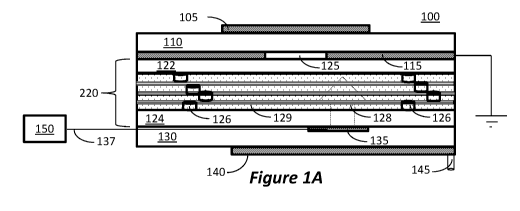
radiation
pattern, wide bandwidth and stable gain is preferred. The use of variable
dielectric
constant materials, specifically liquid crystal (LC) has been proposed in
previous
work. Such antenna generates a scanning RF beam according to the applied
electrical
field force and direction, which can be controlled by software. In this manner
a focal
plane scanning antenna, or a phase shifter in general, is able to maintain its
low
profile and size, without the use of mechanically moving parts. See, e.g., US
7,466,269; US 2014/0266897; US 2018/0062268; and US 2018/0062238.
[0004] For applications where the wavelength of the operating device is in the
microwave range, the required active layer thickness, i.e., the thickness of
the variable
1
CA 03079086 2020-04-14
WO 2019/089634
PCT/US2018/058266
dielectric material (such as liquid crystal), is required to be quite high, 50-
200 p.m,
200-500 p.m, 1000 p.m and even up to several millimeters. In addition, the
response
times of the antenna/phase shifter device, (Ton, Toff), need to be adequate to
support
packet-based beam forming. Various applications, such as a scanning focal
plane
array antenna which is tracking a fast-moving target, or required to monitor
several
moving q stationary targets at the same time, the response times should be
reduced
even further, e.g., to 1 [is or lower. However, the increase in the active
layer
thickness results in an increase in the response times of the system. In a
phase
shifter/antenna device based on nematic liquid crystal materials, or oven
ferroelectrics, the response times are correlated to the active layer
thickness (r) by a
general equation: -collo( r2, which means that a device operating with a very
thick active
layer cannot reach ultra-fast response times, per system requirement.
SUMMARY
[0005] The following summary of the disclosure is included in order to provide
a
basic understanding of some aspects and features of the invention. This
summary is
not an extensive overview of the invention and as such it is not intended to
particularly identify key or critical elements of the invention or to
delineate the scope
of the invention. Its sole purpose is to present some concepts of the
invention in a
simplified form as a prelude to the more detailed description that is
presented below.
[0006] Disclosed aspects of the present invention provide an RF device, e.g.,
antenna
or a phase shifter, variable dielectric-constant (VDC) material layer and a
method for
manufacturing such a device, whereas the VDC layer is made of multiple stacked
sub-
layers, thus providing improved performance and switching time.
[0007] A further aspect of the present invention is to provide an antenna or
an RF
device comprising multiple layers of liquid crystal or other variable
dielectric
material, separated by a thin film or micro-structures, and a method for
manufacturing
such a device, whereas the device homogeneously aligns the liquid crystal
material
between two alignment layers.
[0008] Another aspect of the present invention is to provide a differential
voltage
between the separating multiple VDC films, in order to create a uniform
electric field
2
CA 03079086 2020-04-14
WO 2019/089634
PCT/US2018/058266
between the top and bottom of the antenna device, in order to affectively
change the
dielectric constant of the liquid crystal.
[0009] A further aspect of this invention is to reduce the required voltage
needed to
affectively rotate the liquid crystal molecules, by applying the voltage in
multiple thin
VDC layers, 5-10 p.m, or 10-20 p.m, 20-50 p.m and possibly up to 50-500 p.m.
[0010] Another aspect of the invention is to dramatically reduce the insertion
losses
of the transmission line implemented as the core component for the true time
delay
device. The thickness of the overall VDC layer control that loss, the lower
the height
of the VDC layer the lower the loss.
[0011] In its generic aspect, an antenna is provided which comprises: a
variable
dielectric constant (VDC) layer; a plurality of radiating patches provided
over the
VDC layer; a plurality of signal lines, each terminating in alignment below
one of the
radiating patches; a plurality of control lines, each corresponding to one of
the signal
lines; a ground plane; wherein the VDC layer comprises: a plurality of sub-
layers
stacked one top of each other and separated from each other by thin films.
BRIEF DESCRIPTION OF THE DRAWINGS
[0012] Other aspects and features of the invention would be apparent from the
detailed description, which is made with reference to the following drawings.
It
should be appreciated that the detailed description and the drawings provides
various
non-limiting examples of various embodiments of the invention, which is
defined by
the appended claims.
[0013] The accompanying drawings, which are incorporated in and constitute a
part
of this specification, exemplify the embodiments of the present invention and,
together with the description, serve to explain and illustrate principles of
the
invention. The drawings are intended to illustrate major features of the
exemplary
embodiments in a diagrammatic manner. The drawings are not intended to depict
every feature of actual embodiments nor relative dimensions of the depicted
elements,
and are not drawn to scale.
[0014] Figure 1 is a cross-sectional schematic drawing of a prior art device;
3
CA 03079086 2020-04-14
WO 2019/089634
PCT/US2018/058266
[0015] Figure 1A is a cross-sectional of one embodiment of an antenna using
multiple
VDC sub-layers;
[0016] Figure 1B is an embodiment having two signal lines coupled to each
radiating
patch, while Figure 1C is a top view thereof;
[0017] Figure 1D is a cross-sectional of an embodiment having two VDC layers
and
two ground planes, while Figure 1E is a top view thereof;
[0018] Figure 1F is a cross-sectional of an embodiment having modified layers
order;
[0019] Figure 1G illustrates a cross-section of an embodiment with multiple
radiating
patches
[0020] Figure 1H illustrates a cross-section of an embodiment of a two-
dimensional
array antenna, while Figure 11 is a top view thereof;
[0021] Figure 2 illustrates a cross-section of a VDC made of multiple sub-
layer,
according to the embodiments of the invention, while Figure 2A illustrates an
embodiment wherein the control signal is applied to each of the sublayers
individually
and in a progressive matter of increased voltage.
[0022] Figure 3 illustrates an embodiment for manufacturing the VDC layer.
DETAILED DESCRIPTION
[0023] Embodiments of the inventive RF device will now be described with
reference
to the drawings. Different embodiments or their combinations may be used for
different applications or to achieve different benefits. Depending on the
outcome
sought to be achieved, different features disclosed herein may be utilized
partially or
to their fullest, alone or in combination with other features, balancing
advantages with
requirements and constraints. Therefore, certain benefits will be highlighted
with
reference to different embodiments, but are not limited to the disclosed
embodiments.
That is, the features disclosed herein are not limited to the embodiment
within which
they are described, but may be "mixed and matched" with other features and
incorporated in other embodiments.
4
CA 03079086 2020-04-14
WO 2019/089634
PCT/US2018/058266
[0024] Figure 1 illustrates a prior art RF device, in this example an antenna
100. The
antenna 100 has a radiating patch 105, generally in the form of a copper patch
formed
or adhered to dielectric 110. Figure 1 illustrates a single radiating path,
but generally
the antenna will have a two-dimensional array of radiating patches, such that
Figure 1
can be considered as illustrating only a section of the antenna. Dielectric
110 may be,
e.g., Rogers circuit board material, glass, PET, Teflon, etc. A ground plane
115 is
provided between the bottom of dielectric 110 and the VDC layer 120. A
coupling
window 125 is formed in the ground plane and is used to couple RF energy
between
the radiating patch 105 and the signal line 140. The signal line is coupled to
an output
port, e.g., a coaxial F connector. Thus, RF signal is capacitively coupled
between the
signal line 140 and radiating patch 105, via the intervening dielectric layer
formed by
the VDC layer 120. The VDC layer 120 is formed by a top dielectric layer/film
122,
a bottom dielectric layer/film 124, spacers 126, and liquid crystals 128
dispersed
among the spacers. Note also that the ground plane 115, the VDC layer 120, and
the
signal line 140 form a capacitor, the characteristics of which depends on the
dielectric
constant value of the VDC layer 120.
[0025] Incidentally, as the VDC layer may be formed using liquid crystals, as
a
shorthand the layers may also be referred to herein as liquid crystal (LC)
layers or
sublayers. Similarly, when referring to the VDC material, as a shorthand the
terminology liquid crystal may be used.
[0026] Figure 2 illustrates an embodiment of the overall multi-layer
construction of a
VDC layer 220 that may be used in any device that uses the prior art VDC
layer, such
as VDC layer 120 shown in Figure 1. In Figure 2, power supplier 201 is shown
applying voltage across the top and bottom electrodes 202 and 207, but in
practice the
structure shown would be formed as part of the RF device, as shown in the
other
embodiments disclosed herein. The overall VDC layer 220 is formed of a
plurality of
thin LC sub-layers that are stacked together. Each of the individual VDC
sublayers
may have spacers 203 inserted between and separating dielectric films 205. The
liquid crystals 206 are dispersed among the spacers 203 between a top and
bottom
dielectric films 205. Alignment layers 204 are provided to form the alignment
force
for the LC. The effective dielectric constant, Et, can be calculated using the
individual dielectric constants and the individual heights of each layer, as:
CA 03079086 2020-04-14
WO 2019/089634
PCT/US2018/058266
Et=E1(hi/Ht)*E2(h2/Ht)*E3(h3/Ht); where hi is the height of each individual
sub-layer and Ht is the total height.
[0027] The number and thickness of the sub-layers can be designed so as to
provide
the desired effective dielectric constant. However, since the VDC layer is
formed of
multiple sub-layers, the effective delta c (AE=E0-6-0 is improved, since the
director of
each layer is better aligned both in the off and on conditions. Moreover, the
response
time is improved.
[0028] Figure 1A, illustrates an embodiment combining the multiple VDC sub-
layers
structure shown in Figure 2 with the antenna illustrated in Figure 1. The
elements of
Figure 1A that are similar to those in Figure 1 have the same reference
numerals. As
shown in Figure 1A, the VDC layer 220 is made up of three sub-layers, that are
stacked together. The number of sublayers and the thickness of each sublayer
can be
designed in order to achieve the required performance, such as the required
dielectric
constant in the on and off conditions, and the switching response time. When
needed,
spacers 126 may be used in some or all of the sublayers, such that the
thickness of
each sublayer is maintained according to the required specifications.
[0029] As sown in Figure 1A, electrode 135 is coupled via control line 137 to
a
controller 150, which applies an AC, a DC, or a square-wave DC potential to
the
electrode 135. When the controller applies potential to the electrode 135, an
electric
field (indicated by the broken-line arrow) is formed, which causes the liquid
crystals
128 in the vicinity of the electrode 135 in each of the sublayers to rotate in
an amount
corresponding to the applied potential. Consequently, the characteristics of
the
capacitor formed between the ground plane 115 and the signal line 140 changes.
This
can be used to control the RF signal traveling in the signal line 140, e.g.,
to cause a
delay or phase shift in the signal.
[0030] In the example of Figure 1A, only one radiating patch and one signal
line are
shown, but this arrangement can be repeated in a two-dimensional array to
thereby
form an electronically steerable antenna. In such an arrangement, multiple
control
lines can be provided, one for each of the signal lines. Also, the ground
plane would
have multiple coupling windows, one corresponding to each signal line and its
corresponding radiating patch.
6
CA 03079086 2020-04-14
WO 2019/089634
PCT/US2018/058266
[0031] Thus, according to one embodiment, an antenna is provided, comprising:
a
dielectric plate; at least one radiating patch provided on the dielectric
plate; a ground
plane having at least one window, wherein each radiating patch is aligned with
one
window; at least one signal line, wherein each signal line is configured for
capacitively coupling RF signal to one radiating patch; and a liquid crystal
layer
provided between the signal line and the ground plane and comprising a
plurality of
liquid crystal sublayers stacked together and each made of a top dielectric
film, a
bottom dielectric film, a plurality of spacers provided between the top
dielectric film
and bottom dielectric film, and liquid crystals dispersed among the spacers.
The
spacers may be made of, e.g., glass, PS (polystyrene), PE (polyethylene), PP
(polypropylene), PMMA, Silica, Cellulose acetate, Zirconia.
[0032] Figures 1B and 1C illustrate an embodiment wherein each radiating patch
has
two signal line coupled to it, wherein the two signal lines are orthogonal to
each other.
The elements of the embodiment of Figures 1B and 1B are the same as in the
embodiment of Figure 1A, except that another dielectric layer 132 is provided
below
the first signal line 140, and an orthogonal second signal line 142 is
provided below
the second dielectric layer 132. In this embodiment, one signal line can be
used for
transmission while the other signal line can be used for reception. In another
implementation both signal lines can be used to generate a circularly
polarized signal
by applying the control signal to electrode 135 in a manner that delays the
signal in
one of the signal lines with respect to the other. Of course, as with the
embodiment of
Figure 1A, the embodiment of Figures 1B and 1C can be implemented using a
plurality of radiating patches and corresponding signal and control lines.
[0033] As shown in the example of Figure 1B, the multiple sublayers need not
be of
the same thickness. Each layer may be designed and fabricated to be at
different
thickness, e.g., using different thickness spacers 126.
[0034] Figures 1D and 1E illustrate an embodiment wherein the transmission
characteristics of each signal lines 135, 142, can be controlled
independently.
Notably, this embodiment utilizes two VDC layers 220 and 221, each or both may
be
made of multiple sublayers. Also, this embodiment utilizes multiple ground
planes,
each having windows aligned to couple RF signal between the radiating patch
and the
corresponding signal line. The arrangement can be implemented with multiple
7
CA 03079086 2020-04-14
WO 2019/089634
PCT/US2018/058266
radiating patches, just as with the other embodiments. When implemented as a
two-
dimensional array, the beam can be steered in any direction in hemisphere
space by
the control signals applied to the multiple control lines, so as to
independently control
the delay applied to each signal line.
[0035] As illustrated in Figure 1D, the signal propagating in signal line 140
is
controlled by applying control signal to electrode 135, thus rotating the
liquid crystals
in the stacked multilayer VDC 220, and the signal propagating in signal line
142 is
controlled by applying control signal to electrode 138, thus rotating the LC
in the
stacked multilayer VDC 221. Thus, in one example the signals are delayed by 90
with respect to each other, so as to generate circular polarization.
[0036] The embodiment of Figures 1D and 1E provide an antenna having multiple
VDC layers and multiple ground planes, comprising: a top dielectric layer; a
plurality
of radiating patches provided over the top dielectric layer; a first liquid
crystal layer
positioned below the top dielectric layer; a first ground plane having a
plurality of
windows, each window aligned with one of the radiating patches; a plurality of
first
signal lines each terminating in alignment with one of the radiating patches;
a
plurality of first control lines, each aligned with one of the first signal
lines; a second
liquid crystal layer; a second ground plane having a plurality of windows,
each
aligned with one of the radiating patches; a plurality of second signal lines
each
terminating in alignment with one of the radiating patches; and a plurality of
second
control lines, each aligned with one of the first signal lines; wherein each
of the first
and second liquid crystal layers comprises a plurality of sublayers stacked
together,
each sublayer having a top dielectric, a bottom dielectric, a plurality of
spacers
provided between the top dielectric and bottom dielectric, and a plurality of
liquid
crystals dispersed between the top and bottom dielectrics.
[0037] In some embodiments the layers are arranged in the order, top to
bottom:
radiating patches, top dielectric layer, first ground plane, first liquid
crystal layer, first
control lines, first signal lines, second ground plane, second liquid crystal
layer,
second control lines and second signal lines. Also, as illustrated, various
intermediate
dielectric layers are provided between the various signal lines, control lines
and
ground planes. It should be noted, however, that the illustrated order of
layers is not
mandatory and other orders can be utilized. For example, Figure 1F illustrates
an
8
CA 03079086 2020-04-14
WO 2019/089634
PCT/US2018/058266
embodiment having multiple VDC layers and multiple ground planes, but in a
different order than that of Figure 1D.
[0038] Figure 1F illustrates an embodiment similar to that of Figure 1D,
except that
the order of layers is different. In Figure 1F, the first signal line 140 is
provided
below the radiating patch 105, but above the first ground plane 115 and above
the first
VDC layer 220. The first control line 135 may be provided above or below the
first
VDC layer 220. The first ground plane 115 is provided below the first VDC
layer
220. While in this embodiment the first ground plane 115 has window 125, the
window 125 is for coupling the signals to the second signal line 142 and is
therefore
aligned for the second signal line 142, not the first signal line 140. The
signal for the
first signal line 140 is coupled directly to the radiating patch 105 through
the top
dielectric 110.
[0039] As indicated, the window 125 in the first ground plane is aligned to
couple the
RF signal from the second signal line 142, since the second signal line 142 is
below
the first ground plane, but is above the second VDC layer 221. The second
ground
plane 117 is provided below the second signal line 142 and, therefore,
requires no
windows. The second control line 138 may be provided below or above the second
VDC layer 221.
[0040] Therefore, an RF antenna having multiple ground planes and multiple
variable
dielectric layers is provided, comprising: a top dielectric layer; a plurality
of radiating
patches provided over the top dielectric; a first variable dielectric constant
(VDC)
layer; a first ground plane having a plurality of windows, each aligned with
one of the
radiating patches; a plurality of first signal lines, each terminating below
one of the
windows of the first ground plane; a plurality of first control lines, each
configured to
control liquid crystal domains of the first VDC layer in vicinity of one of
the first
signal lines; a second VDC layer provided below the first VDC layer; a second
ground plane having a plurality of windows, each aligned with one of the
radiating
patches; a plurality of second signal lines, each terminating below one of the
windows
of the second ground plane; and a plurality of second control lines, each
configured to
control liquid crystal domains of the second VDC layer in vicinity of one of
the
second signal lines.
9
CA 03079086 2020-04-14
WO 2019/089634
PCT/US2018/058266
[0041] In fabricating the sublayers for the VDC layer of the RF devices, the
two
opposing dielectric substrates which encapsulate the liquid crystals can be
made of
any non-conduction material desired, whether transparent or opaque, since
there are
no optical considerations. The control electrodes can be made by, e.g.,
deposition
such as evaporation, electroplating, electroless plating, etc., may be printed
on using
conducting ink or paste, etc. As shown in the embodiments disclosed herein,
the
control electrodes may be positioned on either side of the liquid crystals to
generate
the electrical field as required for the function of the RF device. The
control electrode
and signal line materials can be a type of conduction material, specifically
metal, such
as gold (Au), silver (Ag), Titanium (Ti), Copper (Cu), Platinum (Pt), or other
metals
and/or metals layering or alloying. In between the two substrates, spacers
made of
insulating material may be placed to fix and maintain the desired cell gap.
[0042] The liquid crystals sublayers can be produced by roll to roll methods
or using
pre-cut thin dielectric sheets. Figure 3 illustrates a roll-to-roll method of
manufacturing the VDC sublayers according to an embodiment of the invention.
In
Figure 3, supply roll 301 provides a continuous strip of flexible insulating
material
302, e.g., PET, polymer nanocomposites, Pyraltm0 (Available from Du Pont),
ECCOSTOCKO low loss dielectrics (Available from Emerson & Cuming of Laird
PLC, London, England), etc. Meanwhile, supply roll 311 provides a continuous
strip
of insulating material 312, made of same or similar material as strip 302. The
insulating strip 312 is passed through spacer station 305, wherein spacers are
formed
or deposited on the top surface of the insulating strip 312. The insulating
strip 302
passes through aligner station 318 wherein a liquid crystal aligner (e.g., PI
(polyimide), PVA, SiOx, etc.) is deposited or adhered onto the insulating
strip 302.
[0043] In liquid crystal station 308 liquid crystals are deposited onto the
strip 302.
The top and bottom films are then brought together and enter a sealing station
309,
which seals the edges of the insulating strips 302 and 312. After sealing the
film may
be cut to size by sheers 322, and the cut edges may be sealed. The layer are
then
transferred to a stacker 326, which may optionally include adhesive applicator
320,
to form a bond between the sublayers as the VDC film is formed from multiple
sublayers stacked on top of each other.
CA 03079086 2020-04-14
WO 2019/089634
PCT/US2018/058266
[0044] As disclosed above, all of the embodiments shown herein may be
implemented by having multiple radiating patches, a feature illustrated in
Figure 1G,
although for illustration purposes only two radiating patches, 105 and 105a,
are shown
in Figure 1G. In this embodiment, the signal of each radiating patch is fed
independently using signal lines 140 and 140a, via corresponding windows 125
and
125a. Also, the dielectric constant for each signal line is controlled
independently by
corresponding control lines 135 and 135a. Thus, when the multiple radiating
patches
are provided in an array, the dielectric for each signal line can be
controlled
independently, thereby introducing different delay to each line, thus steering
or
scanning the beam.
[0045] As noted above, VDC material has been used in the prior art; however,
in
certain RF and microwave devices, such as antenna, the active layer thickness
must be
relatively high, e.g., 50 to 500 um (as a function of the antenna wavelengths
and
application technology). Higher active layer thickness results in a loss of
the LC
molecules alignment in the bulk, leaving only the LC molecules at both
surfaces that
are close to the alignment layer to be aligned. As a result of that, two
things happen
which degrade the antenna's performance and limit its use. First, since
overall in the
bulk the LC molecules are not aligned (in the voltage "off' state), they are
oriented
freely without a specific direction, and the starting, or voltage "off' state,
dielectric
constant value is higher than for pure planar aligned LC material. When the
voltage is
switched "on", above the threshold value, all LC directors change their
orientation
parallel to the electric field direction, albeit the effect may be stronger at
the edges
than at the bulk layer. The end result, or delta E (AE=E0-E.L) is lower than
what could
be reached if the starting, or "off' state was purely E.L. This loss of delta
E, between
the "on" and "off' stages limits the antenna's performance and capabilities.
Second,
switching times are increased, from milliseconds to seconds when switching the
voltage off, due to the lack of LC alignment at the bulk. Consequently,
current
technology cannot use LC at high thickness, due to lower dielectric
performance and
very slow switching times.
[0046] Conversely, by maintaining each of the active sublayer's thickness low,
e.g.,
5-50 um, the LC molecules are aligned at both surfaces and throughout the
bulk, at
the "off' state, thereby achieving a faster response time (Ton, Toff) and
reduced ci
value, which also corresponds to a higher AE. As a result, the overall
performance of
11
CA 03079086 2020-04-14
WO 2019/089634
PCT/US2018/058266
the phase modulator will be faster and able to achieve a higher phase
modulation, or a
larger beam steering angle. However, the more essential challenge arising for
the
system when using thin LC layers is the high dielectric and ohmic losses of
the
microstrip or stripline signal transmission line, and thus the overall
performance of
the antenna and or device degrades dramatically. Therefore, it is preferred to
use a
very specific and much higher substrate thickness. The total VDC layer's
thickness is
thus achieved by stacking multiple LC sublayers.
[0047] In accordance with disclosed embodiments, low-cost, thin layer liquid
crystal
(LC) phase modulators and phased array antenna designs are provided in which
surface-aligned LCs are modulated reversibly with small applied electrical
fields. The
LC medium of each sublayer is placed in between two surfaces. An alignment
layer
is pre-deposited and pre-conditioned (e.g., by rubbing, photo-alignment,
evaporation,
etc.). A second LC layer is added on top of the thin polymer film, followed by
another thin polymer film. The number of these repeating polymer film and LC
layer
thickness is not set, and can vary between different applications and device
requirements.
[0048] The thin dielectric or polymer film separating the LC layers can be
made of
PE polyethylene, PP polypropelene, ABS, MAYLAR, PET, polyester, PTFE
(including all flouro plastic compounds), Delrin, FEP, PFA, HALCAR ETPE,
Hytrel
(TPE), Polyurethane PU, Cirlex Kapton, Kapton (polyimide) type HN, VN, XC, MT
and all other types of polyimide compounds, Nylon 6/6, PEEK, PEI ULTEM
polyetherimide, PES ULTRASON, PC Polycarbonate, PPS (polyphenylene), PSU
UDEL (Polysulfone Resin), PVDF/KYNAR (polyvynilidene fluoride Resin), Tefzel,
TPX polymethypentene, PS polystyrene and co-polymers of any of the above
mentioned polymers.
[0049] The thickness of the intermediate polymer films is recommended to be
kept as
thin as possible, e.g., 3-10 p.m or 10-25 p.m, up to 25-50 p.m. When using LC
layers,
all surfaces in the device that are in contact with the LC are covered by an
alignment
material, e.g., PI (polyimide), PVA, SiOx, etc. All of the sub-layers are
stacked
together to form the PDLC/SLC layer.
[0050] Construction of the multilayered structure device requires the layers
to be laid
one on top of the other in a parallel and tight thickness control all over the
area of the
device. Spacers, made from material such as glass, PS (polystyrene), PE
12
CA 03079086 2020-04-14
WO 2019/089634
PCT/US2018/058266
(polyethylene), PP (polypropylene), PMMA, Silica, Cellulose acetate, Zirconia,
at the
required diameter, may be distributed evenly on the surface to maintain the
required
gap all over the device area. An aligner film (after alignment material has
been
applied to, and given direction), may be laid upon the spacers.
Adhesive/sealant
material should be applied to the perimeter of the device to seal and prevent
leakage
of the LC material out of the device. Two opposite areas in the perimeter of
the
device may be initially kept without adhesive for LC insertion (by capillary
or liquid
injection, with or without a vacuum). The next layer up is constructed in the
same
manner: spacers are distributed to keep and maintain the gap uniformly,
followed by
another dielectric film. The multi-layer construction is built in this manner,
until the
final layer laid on the gap spheres is the opposite closing dielectric layer,
closing the
device ¨ is laid. After the device layering is complete, LC insertion may take
place.
The final stage is sealing the insertion holes on both sided with a suitable
sealant/adhesive material.
[0051] According to another embodiment, voltage is applied to each individual
thin
film, in a manner that the voltage applied to each film, V1, is smaller than
the total
voltage VT and larger than the lowest voltage VB. By building a multi-layer
structure,
in which the separating films are electrified, an electric field is created
between the
top and bottom layers of the device, but the overall operating voltage of the
device is
reduced. In order to have the separating films act as electrodes, they have to
be made
of metal or metal coated polymer films or have conductive control electrode
applied
to each thin layer. In Figure 2A the variable voltage given to each layer is
depicted,
where VT is the voltage applied to the top dielectric layer, VB is the voltage
applied to
the bottom dielectric layer; Vi and Vi+1 are the voltages applied to the
separating films.
During the "off' state, no voltage is applied to the multilayer structure, in
the "on"
state, voltage is applied in a manner that VT>Vi+1>Vi>VB.
[0052] Thus, a method for fabricating a multi layered phase modulator or
antenna
device separated internally by a thin polymer film coated on both sides by an
alignment layer is provided, comprising: coating an alignment layer on a
bottom
dielectric layer and inducing directivity on the alignment layer; placing
spacers on the
alignment layer; coating a separating film with alignment material on both
sides and
inducing directivity in the alignment material; placing the separating film on
top of
the bottom dielectric layer; placing a second layer of spacers on top of the
separating
13
CA 03079086 2020-04-14
WO 2019/089634
PCT/US2018/058266
film; coating a top alignment layer on a top dielectric film and inducing
directivity in
the top alignment layer and placing the top dielectric layer on top of the
separating
film; and inserting liquid crystals between the bottom dielectric layer and
the
separating film and between the separating film and the top dielectric layer.
[0053] Similarly, a multilayer variable dielectric constant (VDC) device is
provided,
comprising: a bottom dielectric film; a top dielectric layer; at least two VDC
layers
sandwiched between the bottom dielectric layer and the top dielectric layer
and in
physical contact with each other; and, a separation layer positioned between
each two
variable dielectric constant layers. Each of the VDC layers may comprise: a
bottom
liquid crystal (LC) alignment layer; a top LC alignment layer; a plurality of
spacers
dispersed between the bottom LC alignment layer and the top LC alignment
layer; a
plurality of liquid crystals dispersed between the bottom LC alignment layer
and the
top LC alignment layer.
[0054] Figures 1H and 11 illustrate the implementation of the innovative VDC
layer
to a two-dimensional array, having 2x2 radiating patches 105, fed by
corresponding
delay lines 136. As shown in the cross-section of Figure 1H, the delay line is
provided above the VDC layer 220, while the ground plane 115 is provided below
the
VDC layer 220. A signal line 140 couples the signal to the delay line 136 via
the
window 125 in the ground plane 115. The controller 150 applies the control
signal to
the delay line 136, such that the liquid crystals in proximity to the delay
line 136 are
controlled by the signal generated by the controller 150. As noted above, in
an
alternative embodiment the control signal is applied incrementally to each
successive
sublayer of the VDC layer 220.
[0055] It should be understood that processes and techniques described herein
are not
inherently related to any particular apparatus and may be implemented by any
suitable combination of components. Further, various types of general purpose
devices may be used in accordance with the teachings described herein. The
present
invention has been described in relation to particular examples, which are
intended in
all respects to be illustrative rather than restrictive. Those skilled in the
art will
appreciate that many different combinations will be suitable for practicing
the present
invention.
14
CA 03079086 2020-04-14
WO 2019/089634
PCT/US2018/058266
[0056] Moreover, other implementations of the invention will be apparent to
those
skilled in the art from consideration of the specification and practice of the
invention
disclosed herein. Various aspects and/or components of the described
embodiments
may be used singly or in any combination. It is intended that the
specification and
examples be considered as exemplary only, with a true scope and spirit of the
invention being indicated by the following claims.