Note: Descriptions are shown in the official language in which they were submitted.
CA 03079926 2020-04-22
WO 2019/120946 1
PCT/EP2018/083199
A solar cell and a method for manufacturing the solar cell
Technical field
The present invention relates to a solar cell. The present invention also
relates to a method
for manufacturing solar cells.
Background
Dye-sensitized solar cells (DSC) are well known in the art, and work on
similar principles as
photosynthesis. Unlike silicon solar cells, these cells obtain energy from
sunlight using dyes,
which can be manufactured cheap and environmentally friendly.
A dye-sensitized solar cell has a light absorbing layer comprising a porous
metal oxide, for
example a few um thick porous TiO2 electrode layer, dyed by adsorbing dye
molecules and
forming a working electrode. Sunlight is harvested by the dye, producing photo-
excited
electrons that are injected into the conduction band of the metal oxide
particles. Other words
for dye in this context are chromophore, sensitizer and photosensitizer.
There exists different types of dye-sensitized solar cells, such as sandwich
dye-sensitized solar
cells and monolithic solar cells. A sandwich type dye-sensitized solar cell is
normally
manufactured by combining two separately produced parts of a cell by laying
one part of the
cell over the other part. A sandwich type solar cell can comprise a TiO2
electrode layer
deposited onto a first transparent conducting substrate. The first transparent
conducting
substrate normally comprises a transparent conducting oxide layer deposited
onto a glass
substrate. The transparent conducting oxide layer serves the function as an
electron collector
extracting photo-generated electrons from the working electrode. The sandwich
type dye-
sensitized solar cell also has a counter electrode including a second
transparent conducting
substrate attached to the first transparent conducting substrate. The
TiO2electrode layer is in
contact with an electrolyte and the second transparent conducting substrate.
Dye-sensitized solar cells of a monolithic type is, for example, known from WO
2013/149787,
WO 2013/149789, and WO 2014/184379.
Figure la shows an example of a prior art monolithic dye-sensitized solar
cell, known from for
example U59251963, comprising a working electrode including a light absorbing
layer 1, a first
porous conducting layer 2 for extracting photo-generated electrons from the
light absorbing
layer, a porous insulation substrate 4, and a counter electrode including a
second conducting
layer 3 arranged on the opposite side of the porous insulation substrate 4.
The light absorbing
layer 1 may include a porous metal oxide with dye deposited on metal oxide
particles. The
porous insulation substrate 4 is, for example, made of a glass fibres. The
first porous
conducting layer 2 is a layer of a porous conductive material deposited on one
side of the
porous insulation substrate 4. The second conducting layer 3 is a layer of a
porous conductive
material deposited on the other side of the porous insulation substrate 4. The
first and second
CA 03079926 2020-04-22
WO 2019/120946 2
PCT/EP2018/083199
conducting layers are, for example, printed on the porous insulation
substrate. In order to
print the conducting layers onto the porous substrate and to handle the porous
substrate with
the printed layers during production, the porous substrate must have a certain
mechanical
stability. The mechanical stability is normally achieved by controlling the
thickness of the
.. substrate. The porous insulation substrate is electrically insulating. Both
conducting layers 2,
3 comprises particles that are large enough to not penetrate the pores of the
porous
substrate. The porous insulation substrate 4 serves the function of separating
the conducting
layers physically and electrically in order to avoid direct electrical short
circuit between the
conducting layers 2, 3. Further, to allow the first and second conducting
layers 2, 3 to be
printed on the porous substrate, the porous substrate should be suitable for
printing.
The solar cell in figure la is infiltrated with an electrically conducting
medium 5 in the pores
of the light absorbing layer, in the pores of the first and second conducting
layers, and in the
pores of the porous substrate. The conducting medium forms a continuous layer
inside the
pores of the conducting layers, and between the conducting layers inside the
pores of the
porous insulation substrate thereby enabling transport of electrical charge
between the
counter electrode and the working electrode including the light absorbing
layer 1. The first
porous conducting layer extracts the electrons from the light absorbing layer
and transports
the electrons to an external electrical circuit connected to the counter
electrode (not shown
in fig. 1). The counter electrode is used to transfer the electrons to the
conducting medium.
The conducting medium transfer electrons back to the light absorbing layer
thereby
completing the electrical circuit.
Depending on the nature of the conducting medium, either ions or electrons and
holes can be
transported between the counter electrode and the working electrode.
Electrolytes in dye-sensitized solar cells are normally classified as liquid
electrolytes, quasi-
solid-state electrolytes or solid-state electrolytes. The electrolytes can be
in the form of a
liquid, gel or in solid state. There are a large number of electrolytes of
either type known in
.. literature, see for example Chemicals Reviews, Jan 28, 2015, "Electrolytes
in Dye-Sensitized
Solar Cells". The electrolytes are an expensive component of the Dye-
Sensitized Solar Cells.
The counter electrode is normally equipped with a catalytic substance 3' that
serves the
purpose of facilitating the transfer of electrons to the electrolyte.
The conducting medium exhibits a certain electrical resistance to transport
charges. The
electrical resistance increases with the charge transport distance. Therefore,
when electrical
charge is transported between the counter electrode and the light absorbing
layer, there will
always be a certain electrical resistive loss in the conducting medium. By
making the porous
substrate thinner, the resistive losses can be reduced. However, when the
porous substrate
becomes thinner it also becomes more mechanically fragile.
CA 03079926 2020-04-22
WO 2019/120946 3
PCT/EP2018/083199
Figure lb shows another prior art example of a dye sensitized solar cell, as
described in
W02014/184379. This solar cell differs from the solar cell shown in figure la
in that
conducting particles forming a conducting network 6 through the insulating
material has been
inserted in the porous insulating substrate 4. The particles form one or more
electrically
conducting paths through the insulating material of the insulating substrate
4. Due to the
conducting network 6 in the insulating substrate 4, the distance between the
counter
electrode and the light absorbing layer 1 does no longer depend on the
thickness of the porous
substrate 4. Thus, the thickness of the insulating part can be reduced, and by
that the distance
between the counter electrode and the light absorbing layer can be reduced.
Accordingly, the
resistive losses in the conducting medium is reduced. Due to the fact that the
distance
between the counter electrode and the light absorbing layer does no longer
depend on the
thickness of the whole porous substrate but only on the insulating part, it is
also possible to
use a substrate that is thick enough for safe mechanical handling.
Certain conducting media, like copper and cobalt complex electrolytes, can
have very low
electrical conductivity resulting in very large electrical resistive losses.
The low electrical
conductivity originates from the fact that the electrolytes have large ions
with low diffusion
rate. When a liquid electrolyte is to transport charges, the transporting
particles move with
Brownian motion; i.e. they move randomly due to collisions with fast-moving
atoms or
molecules in the liquid. Copper and cobalt have relatively large ions that are
slow moving and
thus have low conductivity. The efficiency of using such electrolytes is
greatly improved by the
above solution.
Another type of solar cell based on disposing a light absorbing layer on top
of a porous
conducting layer, a porous insulating layer and a counter electrode is
described in the co-
pending application WO/5E2017/050016. The light absorbing layer comprises
grains of for
example doped Si. A polymer charge conductor covers the grains of the light
absorbing layer
and extends through the conducting layer and insulating layer to the counter
electrode.
A disadvantage that comes with printing a conducting layer onto a porous
substrate is that
the substrate has to have a thickness that supports the process. Further
handling of the
printed structure during the manufacturing, like conveying or turning sheets
or rolls or heat
treating or stapling the sheets or rolls require the structure to have a
certain mechanical
stability. This is achieved by having a certain thickness of the porous
substrate.
In order to complete the building of the solar cell, a conducting medium is
disposed into the
light absorbing layer, the conducting layer and the porous layer down to the
counter
electrode. The conducting medium is an expensive part of the solar cell.
CA 03079926 2020-04-22
WO 2019/120946 4
PCT/EP2018/083199
Summary
An aspect of the present disclosure is to provide a solution, which seeks to
mitigate, alleviate,
or eliminate one or more of the above and below identified deficiencies in the
art and
disadvantages singly or in any combination. The present disclosure proposes a
device and a
method for minimizing the use of conducting medium in a solar cell.
More specifically, the disclosure provides for a device and a method for
minimizing the use of
conducting medium in solar cells by using an overlapping region of conducting
medium and
conducting and catalytic particles in the substrate without filling the whole
substrate and
counter electrode with conducting medium.
This aspect is achieved by the device and the method as defined in the
independent claims.
According to some aspects of the disclosure, a solar cell is provided. The
solar cell comprises
a working electrode including a porous light absorbing layer, a first porous
conducting layer
for extracting photo-generated electrons from the light absorbing layer,
wherein the light
absorbing layer is arranged on top of the first porous conducting layer, a
counter electrode
including a second conducting layer, a porous substrate disposed between the
first and second
conducting layers, wherein the porous substrate comprises a conducting portion
in electrical
contact with the second conducting layer and an insulating portion disposed
between the first
porous conducting layer and the conducting portion, and a conducting medium
for
transporting charges between the conducting portion and the light absorbing
layer. The
conducting medium is located in the light absorbing layer, in the first porous
conducting layer,
and partly in the porous substrate so that the insulating portion of the
porous substrate
comprises the conducting medium and a first part of the conducting portion
that abuts against
the insulating portion comprises the conducting medium and a second part of
the conducting
portion that abuts against the second conducting layer is free of conducting
medium. In other
words, the porous substrate is partially filled with conducting medium such
that there are
three regions in the porous substrate; one insulating portion with conducting
medium, one
conducting portion with conducting medium and one conducting portion without
conducting
medium. In this way, the use of conducting medium can be minimized. This saves
a lot of cost,
especially in big scale production, and can also enable the use of more
expensive conducting
mediums for better efficiency without significantly increasing the costs.
Also, for the use of
liquid conducting mediums, the risk of leakage can be lowered when smaller
amounts of the
liquid is used.
Due to the conducting portion in the porous substrate, the insulated distance
between the
counter electrode, i.e. the second conducting layer, and the light absorbing
layer does not
depend on the total thickness of the porous substrate. In other words, even
when using a thick
porous substrate, the thickness of the insulating portion 4b can be reduced,
and by that, the
CA 03079926 2020-04-22
WO 2019/120946 5
PCT/EP2018/083199
distance between the counter electrode 3 and the light absorbing layer 1 can
be reduced.
Accordingly, the resistive losses in the conducting medium is reduced. Due to
the fact that the
effective distance for transferring charges between the counter electrode and
the light
absorbing layer does not depend on the thickness of the porous substrate, it
is also possible
to use a substrate that is thick enough for safe mechanical handling. By also
limiting the
presence of the conducting medium to the insulating portion and to the first
part of the
conducting medium, the amount of used conducting medium is minimized. This
makes it
possible to have a substrate thick enough for safe mechanical handling and
lower the cost of
materials since the whole substrate does not need to be filled with conducting
medium.
According to some aspects, the conducting medium is located in pores of the
light absorbing
layer, in pores of the first porous conducting layer, in pores of the
insulating portion of the
porous substrate and in pores of the first part of the conducting portion.
When the conducting
medium is located in the pores of a porous material it is possible for the
conducting medium
to form a continuous chain, such that the conducting medium can efficiently
transport charges
between the conducting portion and the light absorbing layer.
The conducting medium is, for example, a conventional 111-3e1ectr01yte or a
similar electrolyte,
or a Cu/Co - complex electrolyte. Solid state transition metal based complexes
or organic
polymer hole conductors are known conducting mediums.
According to some aspects, the conducting portion comprises catalytic
elements. The catalytic
elements assist in the transfer of charges between the conducting portion and
the conducting
medium.
According to some aspects, the porous substrate comprises a porous insulating
material and
the conducting portion comprises conducting and catalytic particles
accommodated in the
pores and forming a conducting network through the insulating material and
wherein the
conducting medium is in electrical and catalytic contact with the conducting
network in the
first part of the conducting portion. Thus, in the part of the porous
substrate where the
conducting medium and the conducting and catalytic particles overlap, in the
first part, they
are both present in the pores of the porous substrate. This will give good
electrical contact
between the two.
According to some aspects, the distance between the light absorbing layer and
the first part
is between 0.2 um and 60 um, and preferable between 0.8 and 50 um. In other
words, the
conducting medium will transfer charges the maximum distance of 60 um or
preferably 50
um.
According to some aspects, the thickness of the conducting portion is less
than 1 mm, and
preferably less than 100 um. Due to the fact that the conducting portion is
thin, the demand
on the conductivity of the conducting portion is rather low, and lower than
the demand on
the conductivity of the first and second conducting layers.
CA 03079926 2020-04-22
WO 2019/120946 6
PCT/EP2018/083199
According to some aspects, the thickness of the insulating portion is between
0.1 um and 40
um, and preferably between 0.5 um and 20 um. Thus, the electrical resistive
losses in the
conducting medium are reduced and still short circuit is avoided between the
first and third
conducting layer.
According to some aspects, the thickness of the first porous conducting layer
is between 0.1
um and 40 um, and preferably between 0.3 and 20 um. The thickness of the first
porous
conducting layer is advantageously kept thin in order to have a short distance
between the
light absorbing layer and the third conducting layer and the counter
electrode.
According to some aspects, the thickness of the first part of the conducting
portion, is smaller
than the thickness of the second part of the conducting portion. In other
words, the
overlapping part, which is both conducting and comprises conducting medium, is
smaller than
the part which does not comprise conducting medium according to some aspects.
The
overlapping region only needs to be thick enough to allow for electrical
contact between the
conducting portion and the conducting medium. The thinner the overlapping
part, i.e. the first
part, is, the less conducting medium can be used. It should be noted that, the
limit of where
the conducting medium is located in the porous substrate, that is, the line
between the first
and the second part of the conducting portion, is not necessarily a straight
line.
According to some aspects, the thickness of the porous substrate is between 10
um and 1 mm.
Such a layer provides good mechanical strength to the solar cell.
According to some aspects, the insulating portion (4b) is an integral part of
the porous
substrate (4).
According to some aspects, the conducting medium comprises copper ions. Copper
ions, i.e.
Cu2+, Cu, is a non-toxic conducting medium. The use of copper as conducting
medium has
been shown to give a very high resulting photo voltage.
According to some aspects, the average pore size of the porous substrate is
larger than the
average pore size of the first porous conducting layer, and wherein the
average pore size of
the first conducing layer is larger than the average pore size of the light
absorbing layer. This
is advantageous in the production of the solar cell. When using pores that are
smaller on top
and then larger and larger further down the solar cell, capillary action can
be utilized. When
dispensing conducting medium in a liquid or gel form on top of the light
absorbing layer, the
conducting medium does not flow down to the bottom of the solar cell but is
kept in the top
layer by the capillary action until the top layer is filled. This is more
thoroughly explained in
the detailed description when discussing the method for producing the solar
cell.
According to some aspects, examples of conducting and catalytic particles
comprises one or
more of: PEDOT, carbon, platinum, titanium, titanium alloys, nickel, nickel
alloys, carbon
based materials, conducting oxides, conducting nitrides, conducting carbides
and conducting
silicides, platinized FTO, ATO, ITO, carbon black, graphene, or carbon
nanotubes. The
CA 03079926 2020-04-22
WO 2019/120946 7
PCT/EP2018/083199
conducting and catalytic particles comprise for example a conducting core with
a catalytic
shell or coating. Another option is to use particles having a low activation
energy and that are
both conducting and catalytic such as carbon nanotubes, metal carbides, metal
nitrides and
metal silicides.
According to some aspects, the solar cell is a dye-sensitized solar cell. The
light absorbing
element is then a dye as explained in the background. Conventional dyes known
in the art can
be used. A dye is chosen to give good efficiency of the solar cell, especially
in combination
with a copper based conducting medium. The dye can for example be triarylamine
organic dye
comprising any of, or a mixture of, dye in the class Donor-1T bridge-Acceptor
(D-rt-A) and in the
class Donor-Acceptor-1T bridge-Acceptor (D-A-rt-A).
Other types of light absorbing elements like doped Si grains, or grains of
CdTe, CIGS, CIS, GaAs,
perovskite can also be applicable.
The limited amount of conducting medium in the solar cell needed by using the
above design
can make a saving of conducting medium of up to 75 %.
According to some aspects of the disclosure, a method for manufacturing a
solar cell is
provided. The solar cell comprises a first porous conducting layer and a
second conducting
layer and a porous substrate disposed between the first and second conducting
layers. The
method comprises preparing the porous substrate such that the porous substrate
comprises
a conducting portion at a first side of the porous substrate and an insulating
portion at a
second side of the porous substrate, depositing a porous conducting layer on
the second side
of the porous substrate to form the first porous conducting layer, depositing
the second
conducting layer such that the conducting portion is in electrical contact
with the second
conducting layer, depositing a porous semiconducting layer on top of the first
porous
conducting layer to form the light absorbing layer and depositing a conducting
medium onto
the light absorbing layer, and depositing the conducting medium until the
conducting medium
has entered the light absorbing layer, the first porous conducting layer and
partly the porous
substrate so that the insulating portion of the porous substrate comprises the
conducting
medium and a first part of the conducting portion that abuts against the
insulating portion
comprises the conducting medium and a second part of the conducting portion
that abuts
against the second conducting layer is free of conducting medium. The
advantages of the
resulting solar cell is previously discussed. The method is an effective way
of depositing
contacting medium such that it does not fill the whole porous substrate, or
more in particular,
such that it does not fill the conducting portion of the porous substrate.
Another advantage
with this method is that it is easy to manufacture the solar cell according to
the disclosure.
According to some aspects, preparing the porous substrate comprises depositing
a blocking
agent on a second side of the porous substrate, the porous substrate
comprising an insulating
material, to form a blocking layer in a portion of the substrate and
infiltrating the porous
substrate from a first side of the substrate with conducting and catalytic
particles having a size
CA 03079926 2020-04-22
WO 2019/120946 8
PCT/EP2018/083199
smaller than the pore size of the substrate to form a conducting portion. This
is an efficient
method to produce the porous substrate such that is comprises an insulating
portion and a
conducting portion.
According to some aspects, preparing the porous substrate comprises, after
depositing the
first porous conducting layer and the second conducting layer, heat treating
the substrate to
burn off the blocking layer thus forming the insulating portion. Depending on
the blocking
agent used, it may be kept in the insulating portion or burned off after
depositing the first and
second conducting layers. Some blocking agents may not disturb the function of
the solar cell
and then they can be left in the substrate.
According to some aspects, depositing the second conducting layer comprises
depositing an
ink comprising conductive particles on the first side of the porous substrate.
In other words,
the second conducting layer is printed on the first side.
According to some aspects, depositing the second conducting layer comprises
depositing a
metal layer on the first side of the porous substrate. Thus, the second
conducting layer is
deposited as a sandwich construction.
According to some aspects, the conducting medium is comprised in a liquid or
gel. When the
conducting medium is comprised in a liquid or gel it may simplify deposition
of the contacting
medium to the light absorbing layer, the first conducting medium, the
insulating portion and
the first part of the conducting portion.
According to some aspects, the light absorbing layer, the porous substrate and
the first porous
conducting layer are prepared such that the first porous conducting layer has
a pore size that
is smaller than the pore size of the porous substrate and such that the light
absorbing layer
has a pore size that is smaller than the pore size of the first porous
conducting layer and
wherein the capillary action will prevent the liquid or gel from flowing to
the first porous
.. conducting layer until the light absorbing layer is saturated and to the
porous substrate until
the first porous conducting layer is saturated and prevent the liquid or gel
from flowing to the
conducting portion until the insulating portion is saturated and prevent the
liquid or gel from
flowing to the second part of the conducting portion. This method for
depositing the
conducting medium uses capillary action to prevent the contacting medium from
running too
deep in the porous substrate to save the amount of conducting medium used.
According to some aspects, the conducting medium is prevented from entering
the second
part of the conducting portion by polymerizing the liquid or gel before it
reaches the second
part. Polymerizing the liquid or gel is an efficient way of controlling where,
in the solar cell,
the conducting medium is deposited.
CA 03079926 2020-04-22
WO 2019/120946 9
PCT/EP2018/083199
According to some aspects, the polymerization is initiated using any one of,
or a combination
of: UV-light illumination, heating and a two-component process. The choice of
which one to
use depends on the choice of liquid or gel.
Brief description of the drawings
The present technique will be more readily understood through the study of the
following
detailed description of the aspects together with the accompanying drawings,
of which:
Fig. la shows an example of a prior art dye sensitized solar cell as described
in the background.
Fig. lb shows another example of a prior art dye sensitized solar cell as
described in the
background.
Fig. 2 illustrates an example of a dye sensitized solar cell.
Fig. 3 is an illustration of a porous substrate with a conducting portion, an
insulating portion
and overlap of conductive particles in a first part of the conducting portion.
Fig. 4 shows an example of production of the porous substrate and first and
second conducting
layers according to some aspects of the disclosure.
Fig. 5 shows an example of production of the porous substrate and the first
and second
conducting layers using a blocking layer.
The figures are not to scale, emphasis instead being placed on illustrating
the example aspects.
Detailed description
Aspects of the present disclosure will be described more fully hereinafter
with reference to
the accompanying drawings. Like numbers in the drawings refer to like elements
throughout.
The terminology used herein is for the purpose of describing particular
aspects of the
disclosure only, and is not intended to limit the invention. As used herein,
the singular forms
"a", "an" and "the" are intended to include the plural forms as well, unless
the context clearly
indicates otherwise.
Unless otherwise defined, all terms (including technical and scientific terms)
used herein have
the same meaning as commonly understood by one of ordinary skill in the art to
which this
disclosure belongs. It will be further understood that terms used herein
should be interpreted
as having a meaning that is consistent with their meaning in the context of
this specification
and the relevant art and will not be interpreted in an idealized or overly
formal sense unless
expressly so defined herein.
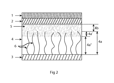
Figure 2 shows an example of a dye-sensitized solar cell according to some
aspects of the
disclosure. The solar cell is preferably a monolithic dye-sensitized solar
cell. A monolithic dye-
sensitized solar cell is characterized in that all layers are directly or
indirectly deposited on one
and the same porous substrate.
CA 03079926 2020-04-22
WO 2019/120946 10
PCT/EP2018/083199
The solar cell comprises a working electrode including a porous light
absorbing layer 1 and a
first porous conducting layer 2 for extracting photo-generated electrons from
the light
absorbing layer. The light absorbing layer 1 and the first porous conducting
layer 2 are porous
layers. The light absorbing layer 1 of the working electrode may include a
porous TiO2
electrode layer deposited onto the first porous conducting layer 2. The TiO2
electrode layer
may comprise TiO2 particles dyed by adsorbing dye molecules on the surface of
the TiO2
particles. According to some aspects, the solar cell is a dye-sensitized solar
cell. The light
absorbing element is then a dye as explained in the background. Conventional
dyes known in
the art can be used. A dye is chosen to give good efficiency of the solar
cell, especially in
combination with a copper based conducting medium. The light absorbing layer
may also
comprise silicon, Si, grains or grains of CdTe, CIGS, CIS, GaAs, perovskite
can also be applicable.
The first porous conducting layer 2 comprises conducting particles and has,
according to some
aspects, a surface layer of TiO2.
The light absorbing layer 1 is arranged on top of the first porous conducting
layer 2. The solar
cell also comprises a counter electrode including a second conducting layer 3
and a porous
substrate 4 disposed between the first and second conducting layers 2, 3. The
porous
substrate 4 comprises a conducting portion 4a in electrical contact with the
second conducting
layer 3. An insulating portion 4b is disposed between the first porous
conducting layer 2 and
the conducting portion 4a. The insulating portion 4b of the porous substrate
prevents short
circuit between the first and second conducting layers because it is
electrically insulating. In
other words, the insulating portion 4b of the porous substrate 4 serves the
function of
separating the conducting layers 2, 3 physically and electrically in order to
avoid direct
electronic short circuit between the conducting layers 2, 3. The conducting
portion 4a forms
an extension of the second conducting layer 3. The first and second conducting
layers 2, 3 are,
for example, printed on the porous substrate. To allow the first and second
conducting layers
2, 3 to be printed on the porous substrate, the porous substrate should be
suitable for
printing. Both conducting layers 2, 3 consist of particles that are large
enough to not penetrate
the pores of the porous substrate. The material forming the conducting layers
2, 3 must have
a suitable corrosion resistance as to withstand the environment in the solar
cell, and
preferably also be resistant to temperatures above 500 C in air without losing
adequate
conductivity. Preferably, the conducting layers 2, 3 are made of a material
selected from a
group consisting of titanium, titanium alloys, nickel, nickel alloys,
graphite, and amorphous
carbon, or mixtures thereof.
It should be noted that the first and second conducting layers 2, 3 are
positioned on a shadow
side of the light absorbing layer 1, i.e. the side opposite the side receiving
the light. Thus, the
first and second conducting layers are positioned on the same side of the
light absorbing layer
as shown in the figures.
The solar cell also comprises a conducting medium 5 for transporting charges
between the
conducting portion 4a and the light absorbing layer 1. The conducting medium
is located in
the light absorbing layer 1, in the first porous conducting layer 2, and
partly in the porous
substrate 4 so that the insulating portion 4b of the porous substrate
comprises the conducting
CA 03079926 2020-04-22
WO 2019/120946 11
PCT/EP2018/083199
medium and a first part 4a' of the conducting portion 4a that abuts against
the insulating
portion comprises the conducting medium and a second part 4a" of the
conducting portion
that abuts against the second conducting layer is free of conducting medium.
In other words,
the porous substrate is partially filled with conducting medium such that
there are three
regions in the porous substrate; one insulating portion with conducting
medium, one
conducting portion with conducting medium and one conducting portion without
conducting
medium. In this way, the use of conducting medium can be minimized. Figure 3
is an
illustration of the porous substrate 4, with the three regions 4a', 4a" and
4b. The conducting
medium 5 is in electrical contact with the conducting portion 4a, in the
figure illustrated as
conducting particles in a network, such that it can transfer charges from the
second
conducting layer 3, via the conducting portion 4a of the porous substrate 4,
to the light
absorbing layer 1. This is cost saving, especially in big scale production,
and can also enable
the use of more expensive conducting mediums for better efficiency without
significantly
increasing the costs. Also, for the use of liquid conducting mediums, the risk
of leakage can be
.. lowered when smaller amounts of the liquid is used. It should be noted that
"free of
conducting medium" means that there is little enough conducting medium such
that the
conducting medium in itself cannot transfer charges. Preferably, the second
part 4a" does not
contain any conducting medium, but in the manufacturing process, it will be
very difficult to
prevent some conducting medium from entering the second part. It should be
further noted
that the second conducting layer is inherently also free of conducting medium
since it is
located below the second part 4a".
Due to the conducting portion 4a in the porous substrate 4, the insulated
distance between
the counter electrode, i.e. the second conducting layer 3, and the light
absorbing layer 1 does
not depend on the total thickness of the porous substrate 4. In other words,
even when using
a thick porous substrate, the thickness of the insulating portion 4b can be
reduced, and by
that, the distance between the counter electrode 3 and the light absorbing
layer 1 can be
reduced. Accordingly, the resistive losses in the conducting medium 5 is
reduced. Due to the
fact that the distance for the charges to travel between the second conducting
layer 3 and the
light absorbing layer 1 does not depend on the thickness of the porous
substrate 4, it is
possible to use a substrate that is thick enough for safe mechanical handling.
By also limiting
the presence of the conducting medium to the insulating portion 4b and to the
first part 4a'
of the conducting portion 4a, the amount of used conducting medium 5 is
minimized. The
limited amount of conducting medium in the solar cell needed by using the
above design can
make a saving of conducting medium of up to 75 %. This makes it even more
possible to have
a substrate thick enough for safe mechanical handling since the whole
substrate does not
need to be filled with conducting medium which can be expensive. Furthermore,
the
effectiveness of the solar cell will not be as sensitive to the choice of
conducting medium. For
example, copper ions, which are easily obtainable but is an expensive, large
and slow ion can
be used more advantageously than before. Due to the fact that the conducting
medium 5 does
not fill the whole porous substrate 4 but only such that it overlaps with, and
is in electrical
contact with, the conducting portion 4a', for example copper ions can be used
advantageously. The porous substrate must allow for fast transport of ions or
holes between
CA 03079926 2020-04-22
WO 2019/120946 12
PCT/EP2018/083199
the electrodes. In order to distribute the conducting medium, the substrate
must have
sufficiently high porosity (pore volume fraction) and low tortuosity.
When the conducting medium 5 is located in the pores of a porous material, the
conducting
medium forms a continuous chain, such that the conducting medium efficiently
can transport
charges between the conducting portion 4a and the light absorbing layer 1. It
should be noted
that the conducting medium 5 is illustrated as random dots in figure 2.
However, it is merely
an illustration of where the conducting medium is present, not how the
particles are actually
positioned. Thus, according to some aspects, the light absorbing layer 1 and
the first porous
conducting layer 2 are porous, and the conducting medium 5 is located in pores
of the light
absorbing layer 1, in pores of the first porous conducting layer 2, in pores
of the insulating
portion 4b of the porous substrate 4 and in pores of the first part 4a' of the
conducting portion
4a. Important features of the finished solar cell product are that the
distance to travel for the
charges between the second conducting layer 3 and the light absorbing layer 1
is short and
that the product is mechanically strong enough for handling.
The first porous conducting layer 2 and the porous substrate 4 are porous to
allow the
conducting medium to penetrate through the conducting layers when the
conducting medium
is applied after the layers have been formed. The conducting medium 5 is for
example a solid-
state hole conductor, or an ionic liquid based electrolyte or a cobalt complex
based
electrolyte. However, the conducting medium can be any suitable conducting
medium. The
conducting medium can be a liquid, a gel, or a solid material such as a
semiconductor.
Examples of electrolytes are liquid electrolytes (such as those based on the 1-
113-, redox couple
or cobalt complexes as redox couple), gel electrolytes, dry polymer
electrolytes and solid
ceramic electrolytes. Examples of semiconductors are inorganic semiconductors,
such as
CuSCN or Cul, and organic semiconductors, such as, e.g., Spiro-OMeTAD.
The conducting medium 5 needs to penetrate through the first porous conducting
layer 2 to
be able to deliver the electrons to the light absorbing layer. Thus, the first
porous conducting
layer needs to have sufficiently high porosity (pore volume fraction) and/or
low tortuosity.
This can be achieved with canals through the layer, with big grains in the
layer, with
monodisperse particles and/or pore forming agents.
Figure 4 is an illustration of a method for manufacturing the solar cell. As
described above, the
solar cell comprises the first porous conducting layer 2 and the second
conducting layer 3 and
the porous substrate 4 disposed between the first and second conducting
layers. The method
comprises preparing Si the porous substrate 4 such that the porous substrate
comprises the
conducting portion 4a at a first side 41 of the porous substrate and the
insulating portion 4b
at a second side 42 of the porous substrate, as shown in the figure as Si. A
porous conducting
layer is deposited S2 on the second side 42 of the porous substrate to form
the first porous
conducting layer 2. The second conducting layer 3 is deposited S3 such that
the conducting
portion 4a is in electrical contact with the second conducting layer and a
porous
semiconducting layer is deposited S4 on top of the first porous conducting
layer 2 to form the
light absorbing layer 1. Details of example ways to deposit the layers will be
described further
CA 03079926 2020-04-22
WO 2019/120946 13
PCT/EP2018/083199
down. This structure has several advantages such as ease of large-scale
manufacturing and
providing a well-defined and constant distance between the second conducting
layer and the
light absorbing layer, when deposited on top of the first porous conducting
layer.
The first side 41 is the bottom side and the second side 42 is the top side of
the porous
substrate 4 as shown in figure 3. As shown in figure 3, the conducting portion
4a is located in
the lower part of the porous substrate 4 and the insulating portion 4b is
located in the upper
part of the porous substrate 4. Thus, the porous substrate 4 comprises two
parts, the
conducting portion 4a and the insulating portion 4b; the conducting portion 4a
is at the first
side 41 of the porous substrate 4 and the insulating portion 4b is at the
second side 42 of the
porous substrate 4. In other words, the conducting portion 4a is located at a
side of the porous
substrate 4 associated with the first side 41 and the insulating portion 4b is
located at a side
of the porous substrate 4 associated with the second side 42.
The porous substrate 4 is, for example, made of microfibers. A microfiber is a
fibre having a
diameter less than 10 um and length larger than 1 nm. Suitably, the porous
substrate
comprises woven microfibers. Ceramic microfibers are fibres made of a
refractory and inert
material, 5i02, A1203 and aluminosilicate. The microfibers may also be glass
microfibers.
Organic microfibers are fibres made of organic materials such as polymers such
as, e.g.,
polycaprolactone, PET, PEO etc, or cellulose such as, e.g., nanocellulose
(MFC) or wood pulp.
The porous substrate 4 may comprise woven microfibers and non-woven
microfibers disposed
on the woven microfibers.
The conducting medium 5 is deposited S4 onto the light absorbing layer 1, and
the conducting
medium is deposited until the conducting medium has entered the light
absorbing layer 1, the
first porous conducting layer 2 and partly the porous substrate 4 so that the
insulating portion
4b of the porous substrate comprises the conducting medium and a first part
4a' of the
conducting portion that abuts against the insulating portion 4b comprises the
conducting
medium and a second part 4a" of the conducting portion that abuts against the
second
conducting layer is free of conducting medium. The advantages of the resulting
solar cell is
previously discussed. The method is an effective way of depositing conducting
medium 5 such
that it does not fill the whole porous substrate 4, or more in particular,
such that it does not
fill the whole conducting portion 4a of the porous substrate. In other words,
the conducting
portion 4a is partially filled with conducting medium 5 such that the
conducting medium is in
electrical contact with the conducting portion. Another advantage with this
method is that it
is easy to manufacture the solar cell according to the disclosure. It should
be noted that if the
depositing of the conducting medium is continued after reaching the first
part, it will continue
to flow to the second part. The amount of deposited conducting media will
therefore be
important.
The conducting medium is for example a conventional l/13 electrolyte or a
similar electrolyte,
or a Cu or Co complex based electrolyte. Solid state transition metal based
complexes or
organic polymer hole conductors are known conducting mediums. According to
some aspects,
the conducting medium is PEDOT.
CA 03079926 2020-04-22
WO 2019/120946 14
PCT/EP2018/083199
As previously discussed, the first and second conducting layers 2, 3 can, for
example, be
deposited by printing. The first porous conducting layer 2 may alternatively
be formed by
evaporation or sputtering of a titanium layer onto the porous substrate, or
any other method
for depositing a thin layer of titanium onto the porous substrate 4. The
second conducting
layer 3 is for example deposited S3 by depositing S3a an ink comprising
conductive particles
on the first side 41 of the porous substrate 4. In other words, the second
conducting layer is
printed on the first side 41. Another alternative is that depositing S3 the
second conducting
layer 3 comprises depositing S3b a metal layer on the first side 41 of the
porous substrate 4.
Thus, the second conducting layer is deposited as a sandwich construction.
The light absorbing layer 1 is deposited onto the first porous conducting
layer 2. The light
absorbing layer is, for example, formed by depositing a porous TiO2 layer onto
the first porous
conducting layer and thereafter adsorb a dye onto the TiO2 layer in the case
that the solar cell
is a dye-sensitized solar cell. The conducting medium 5 is deposited onto the
light absorbing
layer 1 before depositing onto the first porous conducting layer 2 such that
the conducting
medium 5 first fills the light absorbing layer 1 and then continues to fill
the first conducting
medium 2 according to above. The solar cell comprises a light absorbing layer
1 and the
depositing of the conducting medium 5 is done onto the light absorbing layer 1
and then onto
the first porous conducting layer 2 from the light absorbing layer and so on.
Hence, the
conducting medium 5 is located in the light absorbing layer 1, in the first
porous conducting
layer 2, in the insulating portion 4b and in the first part 4a' of the
conducting portion 4a such
that the conducting medium 5 forms a continuous conducting path between the
first part and
the light absorbing layer.
One way of controlling how many layers the conducting medium penetrates, that
is,
controlling the conducting medium 5 such that it does not enter the second
part 4a" of the
conducting portion, is to deposit a predetermined amount of conducting medium
5 onto the
first porous conducting layer 2 or the light absorbing layer 1. The pores of
the light absorbing
layer 1 should be as filled with conducting medium as possible to maximise the
efficiency of
the solar cell. According to some aspects, the conducting medium 5 is
deposited until there is
an adequate electrical connection between the first part 4a' and the light
absorbing layer 1.
In other words, the conducting medium 5 is deposited until there is an overlap
between the
conducting medium 5 and the conducting portion 4a of the porous substrate 4.
Capillary action (sometimes called capillarity, capillary motion, or wicking)
is the ability of
a liquid, or solvent, to flow in narrow spaces without the assistance of, or
even in opposition
to, external forces like gravity. According to some aspects, the average pore
size of the porous
substrate 4 is larger than the average pore size of the first porous
conducting layer 2, and
wherein the average pore size of the first conducing layer 2 is larger than
the average pore
size of the light absorbing layer 1. This is advantageous in the production of
the solar cell.
When using pores that are smaller on top and then larger and larger further
down the solar
cell, capillary action can be utilized. When dispensing conducting medium in a
liquid or gel
form on top of the light absorbing layer or the first porous conducting layer,
depending on the
CA 03079926 2020-04-22
WO 2019/120946 15
PCT/EP2018/083199
method, the conducting medium does not flow down to the bottom of the solar
cell but is
kept in the top layer by the capillary action until the top layer is filled.
As previously discussed, figure 3 is an illustration of an example of the
porous substrate 4,
.. with the three regions 4a', 4a" and 4b. According to some aspects, the
conducting portion
comprises catalytic elements. The catalytic elements assist in the transfer of
charges between
the conducting portion and the conducting medium. It can be seen in the figure
that the
conducting portion 4a comprises a network of particles. Those particles are
conducting
particles and according to some aspects, the porous substrate 4 comprises a
porous insulating
.. material and the conducting portion 4a comprises conducting and catalytic
particles
accommodated in the pores and forming a conducting network 6 through the
insulating
material and wherein the conducting medium is in electrical and catalytic
contact with the
conducting network in the first part of the conducting portion. Thus, in the
part of the porous
substrate 4 where the conducting medium 5 and the conducting and catalytic
particles
overlap, in the first part 4a', they are both present in the pores of the
porous substrate. This
will give good electrical contact between the two. In the figure, the porous
substrate 4
comprises a conducting portion 4a including conducting particles forming a
conducting
network 6 in the insulating material of the porous substrate, and an
insulating portion 4b
without any conducting particles and forming a porous insulating layer. The
insulating portion
.. 4b is here formed as an integral part of the porous substrate 4.
The conducting network 6 is in direct physical and electrical contact with the
second
conducting layer 3 of the counter electrode and will therefore significantly
increase the
conductive surface area of the counter electrode. The conducting surface area
serves the
.. function of transferring electrons or holes from the counter electrode to
the conducting
network. The conducting network in the porous substrate and the thus increased
conductive
surface area of the second conducting layer decrease the charge transfer
resistance between
the conducting medium 5 and the conducting network 6. Additionally, since the
conducting
portion 4a forms a conducting network extending through the insulating
material of the
porous substrate, the distance between the light absorbing layer 1 and the
conducting portion
4a is shorter than the distance between the light absorbing layer 1 and the
second conducting
layer 3. The conducting particles are smaller than the average pore size of
the porous layer 4
in order to be infiltrated effectively.
The conducting particles in the conducting portion 4a may consist of the same
material as is
used in the second conducting layer 3. It is also possible to use other types
of particles such
as carbon based materials (graphite, carbon black, CNT, graphene, etc). It is
also possible to
use other types of particles such as conducting oxides (ITO,FTO, ATO etc) or
carbides, nitrides
or silicides. According to some aspects, the conducting and catalytic
particles comprises one
or more of: PEDOT, carbon, platinum, titanium, titanium alloys, nickel, nickel
alloys, carbon
based materials, conducting oxides, conducting nitrides, conducting carbides,
conducting
silicides, platinized FTO, ATO, ITO, carbon black, graphene, and carbon
nanotubes. The
conducting and catalytic particles comprise for example a conducting core with
a catalytic
shell or coating. The conducting core can be made of metal, metal alloy, metal
oxide, or other
CA 03079926 2020-04-22
WO 2019/120946 16
PCT/EP2018/083199
conducting materials. Another option is to use particles having a low
activation energy and
that are both conducting and catalytic such as carbon nanotubes, metal
carbides, metal
nitrides and metal silicides.
The conducting medium 5 comprises for example ions and according to some
aspects, the
conducting medium 5 comprises copper ions. Copper ions, i.e. Cu2+, Cu, is a
non-toxic
conducting medium and has been shown to give good efficiency, especially in
dye-sensitized
solar cells.
The ions are free moving ions for transferring charges between the counter
electrode and the
light absorbing layer. Another example of ions that may be used as conducting
medium is
cobalt ions. The conducting medium may also be a cobalt based electrolyte, a
cobalt complex
based electrolyte or a copper complex based electrolyte. The conducting medium
comprises
according to some aspects ligands, such as phenanthrolines. The most common
used ion
combination used as electrolyte is the 1113-.
Depending on the nature of the conducting medium, either ions or electrons and
holes, can
be transported between the counter electrode 3 and the working electrode 1.
The conducting
medium 5 may for example be a solid-state hole conductor. A solid-state hole
conductor is,
for example, a semiconductor. An advantage using a hole conductor is that it
is a solid material
and accordingly the requirement of sealing of the solar cell is reduced.
Examples of
semiconductors are inorganic semiconductors, such as CuSCN or Cul, and organic
semiconductors, such as, e.g., P3HT or Spiro-OMeTAD. According to some
aspects, the
conducting medium is a solid-state hole conductor, or an ionic liquid based
electrolyte, or a
cobalt complex based electrolyte. Semiconducting perovskites, like CH3NH3PbI3,
CH3NH3Pb13-
xClx or CH3NH3SnI3or other suitable perovskites can be used.
The thicknesses of the layers of this disclosure will depend on many factors.
Efficiency of the
solar cell is obviously important, such is also the mechanical strength of the
solar cell; it must
be possible to handle both during production and as a finished product without
breaking. But
the required mechanical strength may vary depending on how and where the solar
cell will be
used. The efficiency may also be sacrificed in order to produce a cheaper
solar cell and also
depending on the intended use of the solar cell. Method of manufacturing will
also influence
which thicknesses are possible. Therefore, the thicknesses of the layers may
vary. According
to some aspects, the thickness of the first part 4a' of the conducting portion
4a is smaller than
the thickness of the second part 4a" of the conducting portion. In other
words, the
overlapping part, which is both conducting and comprises conducting medium 5,
is smaller
than the part which does not comprise conducting medium. The overlapping
region only
needs to be thick enough to allow for electrical contact between the
conducting portion and
the conducting medium. The thinner the overlapping part, i.e. the first part,
is, the less
conducting medium 5 can be used. The thickness of the second part 4a" of the
conducting
portion depends on the desired mechanical strength of the packet of layers to
be handled
during manufacturing and the resulting solar cell.
CA 03079926 2020-04-22
WO 2019/120946 17
PCT/EP2018/083199
It should be noted that, depending on the method of manufacture, the limit of
where the
conducting medium is located in the porous substrate, that is, the line
between the first and
the second part of the conducting portion, is not necessarily a straight line.
It should be noted
that by using the method described above, the line will most likely have an
irregular shape
where the conducting medium has entered the porous substrate at different
depths.
As explained, some can be said about the thicknesses of the different layers
but the skilled
person realizes that the thicknesses will depend too much of the
implementation and
manufacturing process of the solar cell for providing exact measurements.
According to some
aspects, the distance between the light absorbing layer 1 and the first part
4a' is between 0.2
um and 60 um, and preferable between 0.8 and 50 um. In other words, the
conducting
medium will transfer charges the maximum distance of 60 um or preferably 50
um. According
to some aspects, the thickness of the conducting portion 4a is less than 1 mm,
and preferably
less than 100 um. Due to the fact that the conducting portion is thin, the
demand on the
conductivity of the conducting portion is rather low, and lower than the
demand on the
conductivity of the first and second conducting layers. According to some
aspects, the
thickness of the insulating portion 4b is between 0.1 um and 40 um, and
preferably between
0.5 um and 20 um. Thus, the electrical resistive losses in the conducting
medium are reduced
and still short circuit is avoided between the first and third conducting
layer. According to
.. some aspects, the thickness of the first porous conducting layer 2 is
between 0.1 um and 40
um, and preferably between 0.3 and 20 um. The thickness of the first porous
conducting layer
is advantageously kept thin in order to have a short distance between the
light absorbing layer
and the third conducting layer and the counter electrode.
According to some aspects, the thickness of the porous substrate 4 is between
10 um and 1
mm. Such a layer provides good mechanical strength to the structure of layers
during
production and to the resulting solar cell.
One way to prepare the porous substrate is illustrated in figure 5. According
to some aspects,
.. preparing 51 the porous substrate 4 comprises depositing 511 a blocking
agent on a second
side 42 of the porous substrate 4, the porous substrate comprising an
insulating material, to
form a blocking layer 7 in a portion 4b of the substrate, and infiltrating S12
the porous
substrate from a first side 41 of the substrate with conducting and catalytic
particles having a
size smaller than the pore size of the substrate to form a conducting portion
4a. This is an
efficient method to produce the porous substrate such that is comprises an
insulating portion
4b and a conducting portion 4a. Using this method forms the network of
conducting particles
6, which has been previously discussed. The blocking agent is either a
material, such as fibres,
that does not affect the function of the solar cell, and can thus be left
there, or it is burned off
after depositing the first and second conducting layers. Therefore, according
to some aspects,
.. preparing 51 the porous substrate 4 comprises, after depositing S2, S3 the
first porous
conducting layer 2 and the second conducting layer 3, heat treating S13 the
substrate to burn
off the blocking layer thus forming the insulating portion 4b. Again,
depending on the blocking
agent used, it may be kept in the insulating portion or burned off after
depositing the first and
CA 03079926 2020-04-22
WO 2019/120946 18
PCT/EP2018/083199
second conducting layers. Some blocking agents may not disturb the function of
the solar cell
and then they can be left in the substrate.
Some of the layers may require heat treatment for sintering them. The light
absorbing layer 1
and the conducting layers 2, 3 may require sintering. The conducting layers 2,
3 may be
sintered in the same heat treatment as the light absorbing layer or earlier.
When the heat
treatment is performed will depend on the material choices. Some conducting
media may be
sensitive to heat treatment and if such a media is used, the heat treatment
should be
performed before depositing the conducting medium.
As previously discussed, capillary action may be used in producing the solar
cells. According
to some aspects, the light absorbing layer 1, the porous substrate 4 and the
first porous
conducting layer 2 are prepared such that the first porous conducting layer 2
has a pore size
that is smaller than the pore size of the porous substrate 4 and such that the
light absorbing
layer 1 has a pore size that is smaller than the pore size of the first porous
conducting layer 2
and wherein the capillary action will prevent the liquid or gel from flowing
to the first porous
conducting layer until the light absorbing layer is saturated and to the
porous substrate until
the first porous conducting layer is saturated and prevent the liquid or gel
from flowing to the
conducting portion 4a until the insulating portion 4b is saturated and prevent
the liquid or gel
from flowing to the second part 4a" of the conducting portion This method for
depositing the
conducting medium 5 uses capillary action to prevent the contacting medium
from running
too deep in the porous substrate 4 to save the amount of conducting medium
used.
There may be several ways to prevent the conducting medium 5 from entering the
second
part 4a" of the conducting portion 4a. One way the conducting medium may be
prevented
from entering the second part 4a" of the conducting portion 4a is by
polymerizing the liquid
or gel before it reaches the second part. Polymerizing the liquid or gel is an
efficient way of
controlling where, in the solar cell, the conducting medium is located.
According to some
aspects, the polymerization is initiated using any one of, or a combination
of: UV-light
illumination, heating and a two-component process. The choice of which one to
use depends
on the choice of liquid or gel. Another way of stopping the conducting medium
from flowing
into the second part 4a" is to use a liquid or gel that hardens by cooling it
or that hardens by
evaporation or polymerizing of parts or all of the gel or liquid matrix. The
process can be
quickened by heating.
When the conducting medium 5 is comprised in a liquid or gel it may simplify
deposition of
the contacting medium to the light absorbing layer, the first porous
conducting layer, the
insulating portion and the first part of the conducting portion. The
conducting medium is for
example comprised in a liquid or gel. The liquid or gel is for example
acetonitrile, CH3CN, ionic
liquid, ionic gel, solvent with dissolved ions or a liquid that changes to gel
depending on
temperature. According to some aspects, the liquid or gel is dried after
deposition such that
ions of the conducting medium are dried into the layers and forming a
conducting chain of
conducting particles.
CA 03079926 2020-04-22
WO 2019/120946 19
PCT/EP2018/083199
Above, some examples of dyes that can be used in the light absorbing layer
have been
discussed in the case that the solar cell is a dye-sensitized solar cell.
There are many dyes that
may be used and according to some aspects, the dye comprises triarylamine
organic dye
comprising any of, or a mixture of, dye in the class Donor-rt bridge-Acceptor
(D-rt-A) and in the
class Donor-Acceptor-rt bridge-Acceptor (D-A-rt-A). Such dyes give good
efficiency of the solar
cell, especially in combination with a copper based conducting medium.
Of the first-class photosensitizer are, for example, substituted
(diphenylaminophenyI)-
thiophene-2-cyanoacrylic acids or substituted (diphenylaminophenyl)cyclopenta-
dithiophene-2-cyanoacrylic acids.
Of the second class are, for example, substituted
(((diphenylaminophenyl)benzothia-diazolyI)-
cyclopentadithiophenyl)aryl/heteroary1-2-cyanoacrylic acids or (((diphenyl-
aminopheny1)-
cyclopentadithiophenyl)benzothiadiazolyparyl/heteroary1-2-cyano-acrylic acids.
Examples of sensitizer, i.e. dyes, which may be used are:
- XY1: (E)-3-(4-(6-(7-(4-(bis(2',4T-bis((2-ethylhexyl)oxy)-[1,1T-
biphenyl]-4-
yl)amino)phenyl)benzo[c][1,2,5]thiadiazol-4-y1)-4,4-bis(2-ethylhexyl)-4H-
cyclopenta[2,1-b:3,4-bldithiophen-2-yl)phenyI)-2-cyanoacrylic acid
- XY1b: (E)-3-(4-(6-(7-(4-(bis(2',4T-dibutoxy-[1,1T-bipheny1]-4-
yl)amino)phenyl)benzo[c][1,2,5]thiadiazol-4-y1)-4,4-bis(2-ethylhexyl)-4H-
cyclopenta[2,1-b:3,4-bldithiophen-2-yl)phenyI)-2-cyanoacrylic acid
- Dyenamo blue: (E)-3-(5-(4-(4-(5-(4-(bis(2',4T-dibutoxy-[1,1T-
bipheny1]-4-
yl)amino)phenyl)thiophen-2-y1)-2,5-bis(2-ethylhexyl)-3,6-dioxo-2,3,5,6-
tetrahydropyrrolo[3,4-c]pyrrol-1-yl)phenyl)furan-2-y1)-2-cyanoacrylic acid
- Dyenamo blue 2016: (E)-3-(5-(4-(4-(5-(4-(bis(2',4T-dibutoxy-[1,1T-
bipheny1]-4-
yl)amino)phenyl)thiophen-2-y1)-2,5-diocty1-3,6-dioxo-2,3,5,6-
tetrahydropyrrolo[3,4-
c]pyrrol-1-yl)phenyl)furan-2-y1)-2-cyanoacrylic acid
- D35: (E)-3-(5-(4-(bis(2',4T-dibutoxy-[1,1T-bipheny1]-4-
yl)amino)phenyl)thiophen-2-y1)-
2-cyanoacrylic acid
- D45: (E)-3-(5-(4-(bis(2',4T-dimethoxy-[1,1T-bipheny1]-4-
yl)amino)phenyl)thiophen-2-
y1)-2-cyanoacrylic acid
- D35CPDT, LEG4: 3-{6-{4-[bis(2',4'-dibutyloxybipheny1-4-yl)amino-]pheny11-
4,4-
dihexyl-cyclopenta-[2,1-b:3,4-bldithiophene-2-y11-2-cyanoacrylic acid
- D51: (E)-3-(6-(4-(bis(2',4T-dimethoxy-[1,1T-bipheny1]-4-yl)amino)pheny1)-
4,4-dihexyl-
4H-cyclopenta[2,1-b:3,4-bldithiophen-2-y1)-2-cyanoacrylic acid
- Y123: 3-{6-{4-[bis(2',4'-dihexyloxybipheny1-4-yl)aminodpheny11-4,4-
dihexyl-
cyclopenta-[2,1-b:3,4-bldithiphene-2-y11-2-cyanoacrylic acid
- JF419: E)-3-(6-(4-(bis(5,7-bis(hexyloxy)-9,9-dimethy1-9H-fluoren-2-
yl)amino)pheny1)-
4,4-dihexy1-4H-cyclopenta[2,1-b:3,4-bldithiophen-2-y1)-2-cyanoacrylic acid
- MKA253: (E)-3-(6-(4-(bis(5,7-dibutoxy-9,9-dimethy1-9H-fluoren-2-
yl)amino)pheny1)-
4,4-dihexy1-4H-cyclopenta[2,1-b:3,4-bldithiophen-2-y1)-2-cyanoacrylic acid
- LO: 4-(diphenylamino)phenylcyanoacrylic acid
CA 03079926 2020-04-22
WO 2019/120946 20
PCT/EP2018/083199
- L1: 5-[4-(diphenylamino)phenyl]thiophene-2-cyanoacrylic acid
- L2: 3-(5-(4-(diphenylamino)styryl)thiophen-2-yI)-2-cyanoacrylic acid
In the following, an example of a method for manufacturing a first example of
a solar cell
according to the invention is described. A porous substrate 4 made of an
insulating material
is infiltrated with conducting and catalytic particles having a size smaller
than the pore size of
the substrate to form a conducting portion 4a of the porous substrate. A layer
of insulating
material is deposited on one side of the porous substrate to form an
insulating portion 4b.
The insulating material is, for example, microfibers made of a ceramic or
organic material. An
ink comprising conductive particles are deposited on the porous insulating
portion to form the
first porous conducting layer 2, and an ink comprising conductive particles
are deposited on
an opposite side of the porous substrate to form the second conducting layer
3. The insulating
layer is, for example, deposited on the porous substrate by screen printing,
slot die coating,
spraying, or wet laying. The porous first and second conducting layers are,
for example,
deposited on the porous substrate by screen printing or any other suitable
printing technique.
A heat treatment may thereafter take place in order to sinter the first and
second conducting
layers. A porous semiconducting layer is printed onto the first porous
conducting layer.
Thereafter, the structure comprising the semiconducting layer, the conducting
portion, the
insulating portion and the first and second conducting layers is heat treated
in order to sinter
the porous semiconducting layer and, if previously not heat treated, also
sintering of the first
and second conducting layers may take place. The semiconducting layer may be
infiltrated by
an ink comprising a dye, thus forming the light-absorbing layer. An ink
comprising the
conducting medium is deposited so that the light-absorbing layer, the first
porous conducting
layer, the insulating layer and an upper part 4a' of the conducting portion is
penetrated by the
conducting medium. The lower part 4a" and the second conducting layer 3 are
not penetrated
by the conducting medium, thus economizing with the conducting medium.
In the following, an example of a method for manufacturing a solar cell
according to the
disclosure is described with reference to figure 4 and 5. Figure 4 and 5
illustrates the
deposition sequences in the manufacturing method.
Step 1: A blocking agent is deposited on a second side 42 of a substrate 4
made of an insulating
material, to form a blocking layer 7 in an insulating portion 4b of the
substrate 4. The blocking
layer is deposited in order to physically prevent the conducting particles
from being infiltrated
all the way to other side of the substrate. Therefore, the blocking layer 7
prevents direct
physical and electrical contact between the first porous conducting layer and
the conducting
particles. The blocking layer may consist of polymers, ceramic particles,
polymer fibres, glass
fibers, carbon nanotubes (CNT), nanocellulose or microfibrillated cellulose
(MFC). It is
advantageous to use fibers as a blocking agent in the blocking layer. It is
advantageous to use
fibres with very small diameter.
Step 2: The porous substrate 4 is infiltrated from a first side 41 of the
substrate with
conducting particles and catalytic particles or particles being both
conductive and catalytic
CA 03079926 2020-04-22
WO 2019/120946 21
PCT/EP2018/083199
having a size smaller than the pore size of the substrate to form a conducting
portion 4a in a
first portion of the substrate.
Step 3: An ink comprising conductive particles is printed on the second side
42 of the porous
substrate 4 to form the first porous conducting layer 2.
Step 4: An ink comprising conductive particles is printed on the first side 41
of the porous
substrate 4 to form the second conducting layer 3.
Step 5: The structure is heat treated to burn off the blocking layer 10 thus
forming the
insulating portion 4b and the conducting portion 4a.
Step 6: A TiO2 electrode layer is deposited onto the first porous conducting
layer 2 to form
the working electrode, i.e. the light absorbing layer 1.
Step 7: The structure is heat treated to sinter the TiO2 electrode. The
conducting layers 2, 3
may be sintered in the same heat treatment step or in an earlier step.
Step 8: The TiO2 electrode is infiltrated with a dye.
Step 9: A conducting medium is deposited so that the pores of the TiO2 layer,
i.e. the light
absorbing layer 1, the first porous conducting layer 2, the insulating portion
4b and the first
part 4a' of the conducting portion are filled with conducting medium. The
second part (4a")
of the conducting portion is kept at a lower temperature, thus preventing the
conducting
.. medium to penetrate down to that part.
The invention is not limited to the above described example and can be varied
within the
scope of the claims. As an example, materials used for the different layers
may vary depending
on desired efficiency/cost ratio and on availability of different materials.
Further, the method
for manufacturing a solar cell can be carried out in many different ways
within the scope of
the claims. For example, there are many different kinds of chemical treatments
that can be
performed on the different layers of the solar cell but such treatments are
not relevant to the
described invention.
List of reference numbers:
1: light absorbing layer
2: first porous conducting layer
3: second conducting layer
3': catalytic substance
4: porous substrate
41: first side
42: second side
4a: conducting portion
CA 03079926 2020-04-22
WO 2019/120946 22
PCT/EP2018/083199
4a': first part of the conducting portion
4a": second part of the conducting portion
4b: insulating portion
5: conducting medium
6: conducting network
7: blocking layer