Note: Descriptions are shown in the official language in which they were submitted.
CA 03080320 2020-04-24
WO 2019/084408 PCT/US2018/057717
PULSE-DRIVEN CAPACITIVE DETECTION FOR FIELD-EFFECT TRANSISTORS
CROSS-REFERENCE TO RELATED APPLICATIONS
[0001] This application claims priority to Indian Patent Application No.
201721038194,
entitled "PULSE-DRIVEN CAPACITIVE DETECTION FOR FIELD-EFFECT
TRANSISTORS (FET)," filed October 27, 2017, the content of which is
incorporated by
reference herein in its entirety.
STATEMENT REGARDING FEDERALLY SPONSORED
RESEARCH OR DEVELOPMENT
[0002] This invention was made with government support under grant No. IIP-
1434059
awarded by the National Science Foundation. The Government has certain rights
in the
invention.
BACKGROUND
[0003] Recently, lead contamination and related health hazards has raised a
serious global
issue. Direct intake of lead through drinking water on a daily basis can
affect the central nervous
system, and the hematopoietic, hepatic, and renal systems. An alarming level
of increase of lead
was found in the blood of people living in the city of Flint, Michigan, USA
due to the poor
conditions of the water supply system (lead leak from the pipeline during the
water conveyance).
Conventional tests such as inductively coupled plasma mass spectrometry (ICP-
MS), atomic
absorption spectroscopy (AAS), and atomic emission spectrometry (AES) are
costly due to their
long procedure, bulky setup, and need for a professional operator.
Electrochemical stripping
analysis using voltammetry has also been successfully used for measuring
various metal ions in
trace level selectively with high reproducibility. However, it is limited by
working electrode
maintenance with proper cleaning, reduction/oxidation potential peak position
drifting due to the
aging of the reference electrode, and background current instability. Also,
the presence of a high
concentration of common metal ions in real water can significantly impact the
results.
Therefore, rapid, portable, low cost automated detection of lead ions in water
is in great demand.
SUMMARY
1
CA 03080320 2020-04-24
WO 2019/084408 PCT/US2018/057717
[0004] The disclosure provides a system for detecting ions in a sample. In
one embodiment,
the system includes a field-effect transistor sensor and an electronic
controller. The field-effect
transistor sensor is in contact with the sample and includes a first electrode
and a second
electrode. The electronic controller is coupled to the field-effect transistor
sensor. The
electronic controller is configured to apply a pulse wave excitation signal to
the first electrode.
The electronic controller is also configured to receive a response signal from
the second
electrode. The electronic controller is further configured to determine an
electrical characteristic
of the field-effect transistor sensor based on the response signal. The
electronic controller is also
configured to determine an amount of the ions in the sample based in part on
the electrical
characteristic of the field-effect transistor sensor.
[0005] The disclosure also provides a method for detecting ions in a
sample. In one
embodiment, the method includes contacting a field-effect transistor sensor
with the sample.
The method also includes applying a pulse wave excitation signal to a first
electrode of the field-
effect transistor sensor with an electronic controller. The method further
includes the electronic
controller receiving a response signal from a second electrode of the field-
effect transistor
sensor. The method also includes determining, with the electronic controller,
an electrical
characteristic of the field-effect transistor sensor based on the response
signal. The method
further includes determining, with the electronic controller, an amount of the
ions in the sample
based on the electric characteristic of the field-effect transistor sensor.
[0006] The disclosure also provides a pulse-driven capacitance measurement
system
including a field effect transistor (FET) to measure small concentrations of
solutes in liquid and
gas solutions. In general, the signal from the FET-based sensor device is
transduced through
resistance/current measurements considering the channel as a chemi-resistor.
[0007] Other aspects of the disclosure will become apparent by
consideration of the detailed
description and accompanying drawings.
BRIEF DESCRIPTION OF THE DRAWINGS
[0008] FIG. 1 is a diagram of a detection system for detecting ions, in
accordance with some
embodiments.
2
CA 03080320 2020-04-24
WO 2019/084408 PCT/US2018/057717
[0009] FIG. 2 is a diagram of an electronic controller included in the
detection system of
FIG. 1, in accordance with some embodiments.
[0010] FIG. 3 is a flowchart of a method for detecting ions in a sample, in
accordance with
some embodiments.
[0011] FIG. 4 is a diagram of a field-effect transistor sensor, in
accordance with some
embodiments.
[0012] FIG. 5A is a diagram of a field-effect transistor measurement sensor
with back-gate
potential, in accordance with some embodiments.
[0013] FIG. 5B is a diagram of a pulse measurement circuit with zero back-
gate potential, in
accordance with some embodiments.
[0014] FIG. 5C is a graph of a square pulse wave and its transient waveform
in the presence
of DI water and Pb2+ solution.
[0015] FIG. 5D is a graph of normalized pulse waves.
[0016] FIG. 5E is a graph of waveform reproducibility in the presence of
water and under
drying conditions.
[0017] FIG. 6 is a diagram of a microcontroller-based pulsed-controlled
portable capacitance
measurement system, in accordance with some embodiments.
[0018] FIG. 7A is an image of reduced graphene oxide sheets bridging
interdigitated
electrodes at a low magnification.
[0019] FIG. 7B is an image of reduced graphene oxide sheets bridging
interdigitated
electrodes at a high magnification.
[0020] FIG. 7C is an image of a single layer graphene oxide channel on an
electrode.
[0021] FIG. 7D is a graph of example Raman spectrum of graphene oxide
nanosheets.
3
CA 03080320 2020-04-24
WO 2019/084408 PCT/US2018/057717
[0022] FIG. 7E is an image of sputtered gold nanoparticles on the surface
of an aluminum
oxide layer.
[0023] FIG. 7F is a graph of IV characteristics of an example field-effect
transistor sensor.
[0024] FIG. 8A is a diagram of a pulse generation and measurement circuit,
in accordance
with some embodiments.
[0025] FIG. 8B is a diagram of a packaged portable meter with an integrated
micro-sensor
chip, in accordance with some embodiments.
[0026] FIG. 9A is a graph of a reversibility test in DI water and under
drying conditions, in
accordance with some embodiments.
[0027] FIG. 9B is a graph of a stabilization test of the sensor in DI
water, in accordance with
some embodiments.
[0028] FIG. 9C is a graph of a real time Pb2+ testing result with a
microcontroller based
measurement system, in accordance with some embodiments.
[0029] FIG. 10A is a graph of real-time resistance measurement data of a
FET sensor in DI
water for a background and stabilization test, in accordance with some
embodiments.
[0030] FIG. 10B is a graph of resistance transients with bi-direction
response for a lead ion.
[0031] FIG. 10C is a graph of resistance transients with bi-direction
response for a lead ion.
[0032] FIG. 11A is a graph of response% versus concentration for an example
calibration, in
accordance with some embodiments.
[0033] FIG. 11B is a graph of real time transient data for a selectivity
test for Hg2+ and
mixed ions measurements, in accordance with some embodiments.
[0034] FIG. 12A is a graph of real-time measurement capacitance transients
of common
metal ions.
4
CA 03080320 2020-04-24
WO 2019/084408 PCT/US2018/057717
[0035] FIG. 12B is a graph of real-time measurement capacitance transients
of heavy metal
ions with mixed ions.
[0036] FIG. 13A is a graph of responses for Pb' and other individual and
mixed metal
cations.
[0037] FIG. 13B is a graph of testing results of real water samples.
[0038] FIG. 13C is a graph of real-time capacitance transients of different
real water
samples.
[0039] FIG. 13D is a graph of predicted lead ion concentrations from
sensors with standard
vales from ICP measurements, in accordance with some embodiments.
[0040] FIG. 14A is a diagram of a model of an insulated GFET structure with
attached
probes in a Pb' solution, in accordance with some embodiments.
[0041] FIG. 14B is a diagram of an equivalence circuit model of a field
effect transistor
structure, in accordance with some embodiments.
DETAILED DESCRIPTION
[0042] Before any embodiments of the disclosure are explained in detail, it
is to be
understood that the disclosure is not limited in its application to the
details of construction and
the arrangement of components set forth in the following description or
illustrated in the
following drawings. The disclosure is capable of other embodiments and of
being practiced or of
being carried out in various ways.
[0043] Graphene as a representative 2D material is found to be promising
for FET-based
sensor applications due to its unique one atomic layer structure, high
specific surface area, great
signal/noise ratio, excellent mechanical strength, and small size. Chemical
exfoliation in the
liquid phase may produce one atomic layer thickness of ultrafine nanosheets in
large scale from
bulk graphite. The high surface area of graphene may be functionalized with
various ligands to
attract metal ions, biomolecules, and gas species for sensing applications.
Micropatterned,
protein-functionalized reduced graphene oxide (rGO) film may be used as a
sensing
CA 03080320 2020-04-24
WO 2019/084408 PCT/US2018/057717
semiconductor channel to realize lead ion (Pb2+) real-time detection. A self-
assembly method for
constructing an rGO sensing platform for Pb2+ monitoring may also been used.
In general, the
signal from such a FET-based sensor device is transduced through
resistance/current
measurements considering the channel as a chemi-resistor. One potential
problem is that the
continuous voltage across ultrathin 2D nanomaterials can generate heat and
modify the intrinsic
conductivity, which leads to a long stabilization time and signal drift. This
unsaturated baseline
with continuous drift is incompatible with rapid evaluation and interferes the
response in the
presence of analytes, thereby increasing the measurement error. In
addition, the
resistance/current response% (i.e., change percentage in resistance or current
due to sensing
events) to analytes is always relatively low, which may also lead to notable
errors in practice.
Examples of response% are illustrated below in Table 1.
TABLE 1- COMPARISON OF CAPACITANCE-BASED SENSING PERFORMANCE
Concentration
Sensing Materials and Detected (nM) Response
Selectivity' (
Test Method and Chemical (%) k target ¨other)
Target
kpb2+_Hg2+(10 M) = 3.3
rGo/GSH-AU NPs (DC) 10 nM Pb2+ 1.7% kpb2+_zn2+(10 /AM) = 30
Ti3C2-MXene (DC) 100 nM 1 <0.01%
dopamine
0.04 x 10⁻⁶ nM
Graphene/olfactory
odorant (amyl <2%
receptors (DC)
butyrate)
PII2T-Si polymer/33-
10,000 nM kHg
probe-Au NPs (DC) 2+¨Pb2+ (1 /AM) = 3.2
based thiolated DNA 10%
Hg2+ kHg2+¨Zn2+ (1 /AM) = 2.7
k H202(0.05 mM)¨Uric acid(1 mM) = 3.3
k H202(0.05 mM)¨Ascorbic acid(1 mM) = 5.7
Polypyrrole/rGO (DC) 0.1 nM H202 1.4%
kH202(0.05mM)¨Ascorbic acid(1 mM)
= 22.8
Pt NPs/rGO (DC) 2.4 nM SsDNA <0.01%
Bismuth-coated carbon
electrodes (stripping 1-150 ppb Pb2+
voltammetry)
rGO/GSH-AU NPs
12 nM Pb2+ 347% kPb 2+ ¨Hg 2 ,Fe 3+Mg 2 ,Zn2
,Na+ (48 nM)
(Pulse) ¨(10
¨ 30)
ak targ e t ¨ o the r is the ratio of signal response to target and other
chemicals.
6
CA 03080320 2020-04-24
WO 2019/084408 PCT/US2018/057717
[0044] Therefore, an alternative strategy is needed to address these
issues. The continuous
voltage across the sensor can be replaced with a periodic square pulse wave
(for example, using
a function generator). In the presence of analytes, the sensing signal across
the sensor quickly
changes to stable slanting charge/discharge transients that represent a high
capacitive influence.
Upon drying the solution, the signal again regains its pure square wave
instantly. Further, a
pulsed signal in combination with capacitance measurement may be used to
capture the rapid
change in a signal in the presence of analytes using, for example, a graphene
field-effect
transistor (GFET) sensor. A pulsed capacitance measuring system with a
programmed
microcontroller may be used to evaluate the sensing performance of the
disclosed system. The
disclosed capacitance-based portable device with simple droplet-based
measurement system
shows rapid stabilization in background deionized water (DI water), negligible
drift, high
sensitivity, and selectivity toward lead ion detection in real-time
measurements.
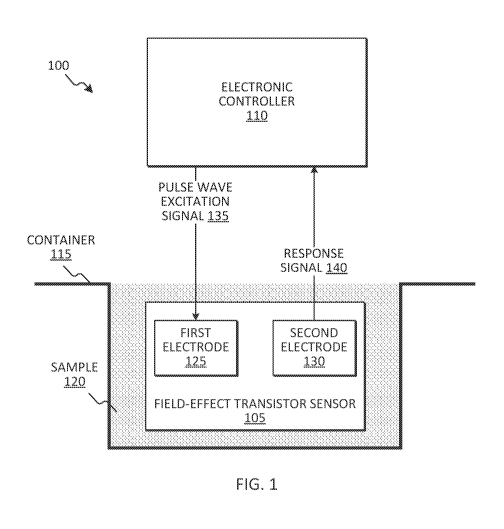
[0045] FIG. 1 is a diagram of one example embodiment of a detection system
100. In the
embodiment illustrated in FIG. 1, the detection system 100 includes a field-
effect transistor
sensor 105 and an electronic controller 110. Electrical characteristics of the
field-effect
transistor sensor 105 change when the field-effect transistor sensor 105
interacts with an analyte.
For example, the capacitance of the channel of the field-effect transistor
sensor 105 changes
when the field-effect transistor sensor 105 is submerged in a container 115
containing a sample
120 (or solution) that includes lead ions, as illustrated in FIG. 1. In the
embodiment illustrated in
FIG. 1, the sample 120 is a liquid medium. Alternatively or in addition, the
sample 120 may
include a different medium such as a gas medium.
[0046] The field-effect transistor sensor 105 illustrated in FIG. 1
includes a first electrode
125 (for example, a source terminal) and a second electrode 130 (for example,
a drain terminal).
The electronic controller 110 is coupled to field-effect transistor sensor
105. The electronic
controller 110 applies a pulse wave excitation signal 135 to the first
electrode 125. Responsive
to the pulse wave excitation signal 135, the field-effect transistor sensor
105 generates a response
signal 140. The electronic controller 110 receives the response signal 140 via
the second
electrode 130.
7
CA 03080320 2020-04-24
WO 2019/084408 PCT/US2018/057717
[0047] FIG. 2 is a diagram of one example embodiment of the electronic
controller 110. In
the embodiment illustrated in FIG. 2, the electronic controller 110 includes
an electronic
processor 205 (for example, a microprocessor), memory 210, an input/output
interface 215, a
signal generator circuit 220, a sensor circuit 225, and a bus. In alternate
embodiments, the
electronic controller 110 may include fewer or additional components in
configurations different
from the configuration illustrated in FIG. 2. The bus connects various
components of the
electronic controller 110 including the memory 210 to the electronic processor
205. The
memory 210 includes read only memory (ROM), random access memory (RAM), an
electrically
erasable programmable read-only memory (EEPROM), other non-transitory computer-
readable
media, or a combination thereof. The electronic processor 205 is configured to
retrieve program
instructions and data from the memory 210 and execute, among other things,
instructions to
perform the methods described herein. Alternatively or in addition, the memory
210 is included
in the electronic processor 205.
[0048] The input/output interface 215 includes routines for transferring
information between
components within the electronic controller 110 and other components of the
detection system
100, as well as components external to the detection system 100. The
input/output interface 215
is configured to transmit and receive signals via wires, fiber, wirelessly, or
a combination
thereof. Signals may include, for example, information, data, serial data,
data packets, analog
signals, or a combination thereof.
[0049] The signal generator circuit 220 is configured to generate the pulse
wave excitation
signal 135. As used herein, the term "pulse wave" is defined as a non-
sinusoidal waveform that
includes square waves (i.e., duty cycle of 50%) and similarly periodic but
asymmetrical waves
(i.e., duty cycles other than 50%). In some embodiments, the pulse wave
excitation signal 135
includes a direct current square wave. As used herein, the term "direct
current square wave" is
defined as a signal with a constant polarity and in which the amplitude of the
signal alternates at
a substantially steady frequency between fixed minimum and maximum values,
with
substantially the same duration at the minimum and maximum values. In
alternate embodiments,
the pulse wave excitation signal 135 includes a direct current rectangular
wave. As used herein,
the term "direct current rectangular wave" is defined as a signal with a
constant polarity and in
which the amplitude of the signal alternates at a substantially steady
frequency between fixed
8
CA 03080320 2020-04-24
WO 2019/084408 PCT/US2018/057717
minimum and maximum values, with different durations at the minimum and
maximum values.
The pulse wave excitation signal 135 is distinct from a continuous direct
current signal in which
the voltage of the signal is substantially constant. The pulse wave excitation
signal 135 is also
distinct from a pulsed (or pulsating) direct current signal in which the
voltage of the signal
changes but is still substantially constant. In some embodiments, the signal
generator circuit 220
includes, among other things, a function generator, resistors, rectifiers,
amplifiers, digital-to-
analog converters, voltage-to-current converters, or a combination thereof.
[0050] The sensor circuit 225 is configured to measure one or more
electrical characteristics
of the response signal 140 such as voltage and current. In some embodiments,
the sensor circuit
225 includes, among other things, an oscilloscope, resistors, filters,
amplifiers, analog-to-digital
converters, current-to-voltage converters, or a combination thereof.
[0051] The electronic controller 110 is configured to determine an
electrical characteristic of
the field-effect transistor sensor 105 based on the response signal 140. For
example, the
electronic controller 110 may determine a capacitance of the field-effect
transistor sensor 105
based on the response signal 140. In some embodiments, the electronic
controller 110 is
configured to determine an electrical characteristic of the field-effect
transistor sensor 105 based
on a signal characteristic of the response signal 140. For example, the
electronic controller 110
may determine a capacitance of the field-effect transistor sensor 105 based on
a time constant of
the response signal 140. In some embodiments, the electronic controller 110 is
configured to
determine a signal characteristic of the response signal 140 based on a change
in an electrical
characteristic of the response signal 140. For example, the electronic
controller 110 may
determine a time constant of the response signal 140 based on a change in the
voltage of the
response signal 140. In some embodiments, the electronic controller 110 is
configured to
determine an electrical characteristic of the response signal 140 using
measurements (for
example, voltage and current measurements) from the sensor circuit 225. The
electronic
controller 110 is configured to determine an amount of the ions in the sample
120 based on an
electric characteristic of the field-effect transistor sensor 105. For
example, the electronic
controller 110 may determine an amount of ions in the sample 120 based on the
capacitance of
the field-effect transistor sensor 105.
9
CA 03080320 2020-04-24
WO 2019/084408 PCT/US2018/057717
[0052] FIG. 3 illustrates an example method 300 for detecting ions in a
sample. The method
300 is described with respect to the components illustrated in FIGS. 1 and 2.
However, it should
be understood that in some embodiments, all or portions of the method 300 may
be implemented
with other components. At block 305, the field-effect transistor sensor 105 is
contacted with the
sample 120. For example, in some embodiments, a drop of a liquid solution
containing lead is
poured onto the field-effect transistor sensor 105. At block 310, the
electronic controller 110
applies the pulse wave excitation signal 135 to the first electrode 125 of the
field-effect transistor
sensor 105. For example, in some embodiments, the signal generator circuit 220
generates a
direct current square wave signal that is applied to the first electrode 125
of the field-effect
transistor sensor 105. At block 315, the electronic controller 110 receives
the response signal
140 from the second electrode 130 of the field-effect transistor sensor 105.
At block 320, the
electronic controller 110 determines an electrical characteristic of the field-
effect transistor
sensor 105 based on the response signal 140. For example, in some embodiments,
the electronic
controller 110 determines a capacitance of the field-effect transistor sensor
105 based on the
response signal 140. At block 325, the electronic controller 110 determines an
amount of the
ions in the sample 120 based on the determined electric characteristic of the
field-effect transistor
sensor 105. In some embodiments, the ions are lead ions. Alternatively or in
addition, the ions
are ions of another analyte such as mercury.
[0053] FIG. 4 is a diagram of one example embodiment of a field-effect
transistor sensor
400. In the embodiment illustrated in FIG. 4, the field-effect transistor
sensor 400 includes a
source terminal 405, a drain terminal 410, a back gate 415, and a top gate
420. The source
terminal 405 and the drain terminal 410 comprise highly conductive materials
such as noble
metals (for example, Au, Pd, Ag, and Pt) or graphene. The back gate 415 is
used to characterize
the electronic properties (for example, current on/off ratio) of the field-
effect transistor sensor
400. In the embodiment illustrated in FIG. 4, the back gate 415 includes a
conductive under-
layer 425 (such as Si or a conductive polymer) and an over-layer 430 (such as
5i02) to create a
capacitive effect. In some embodiments, the back gate 415 is manufactured by
cutting a silicon
ingot and generating the over-layer 430 on the silicon wafer in situ. The top
gate 420 isolates the
analytes from the electrodes and prevents short circuit current from the
solvent or other
conducting species in the solvent. The top gate 420 can also prevent non-
specific adhesion of
CA 03080320 2020-04-24
WO 2019/084408 PCT/US2018/057717
analytes to the channel material. In the embodiment illustrated in FIG. 4, the
top gate 420
includes a reduced graphene oxide layer 435 coated with a passivation layer
440 (for example,
SiO2 or other insulating metal oxide including A1203, TiO2, and SrTiO3). The
reduced graphene
oxide layer 435 acts as a conducting channel suspended above the back gate 415
and electrically
connects the source terminal 405 and the drain terminal 410. Gold
nanoparticles 445 are in
contact with the passivation layer 440. In some embodiments, the gold
nanoparticles are discrete
nanoparticles. One or more probes 450 are bound to each of the gold
nanoparticles 445. Lead
ions 455 bond with the probes 450.
[0054] In some embodiments, a square pulse wave source is used to detect
Pb' ion
concentrations using a graphene FET device as shown in FIGS. 5A and 5B. During
the sensing,
the back gate voltage is removed and Pb' ions adsorbed by a glutathione (GSH)
probe from the
top gate create a voltage effect through an induced positive electrostatic
field. The capacitance
measurement is performed with a square pulse wave-based technique that
calculates the time
constant of the morphed signal across the drain-source interface of the sensor
which is connected
in series with a reference resistor. With the known value of resistance
(Rref), the capacitance
value can be obtained by measuring the time constant (T). In some embodiments,
a standard
function generator generates the short duration square pulse and the FET
sensor output signal
resembles a perfect square wave in air. In some embodiments, the signal
changes across the
drain source interface in the presence of water and the addition of aqueous
metal ions are
visualized using a digital oscilloscope. An example of a square pulse wave and
its transient
waveform in the presence of deionized (DI) water and Pb' is illustrated in
FIG. 5C. When a
drop of deionized water is exposed on the surface of the sensor, the signal
quickly becomes
slanted. While not wishing to be bound by a particular theory, the voltage
transient across the
sensor looks like a capacitive behavior in a RC circuit due to slow charging
and discharging.
The time constant (T) is estimated by calculating the time to reach 63.2%=1/e
value of the
maximum change in the charging/discharging voltage. Upon injection of the Pb"
ion solution,
the transient becomes more slanted due to the adsorption of lead ions by the
GSH probes on the
sensor surface which change the capacitance and the corresponding time
constant. FIG. 5D
shows the normalized plot of the signal in the presence of air, water, and a
Pb' solution. The
time constant of the sensor in water (TO and in a lead solution (T2) increased
systematically with
11
CA 03080320 2020-04-24
WO 2019/084408 PCT/US2018/057717
respect to the blank sensor (air). The responses in DI water and Pb' sample
from blank sensor
state (air) are also very fast. The square wave is recovered upon removal of
water sample as
illustrated in FIG. 5E. In view of this, it is understood that this transient
information through
relative change in capacitance may be utilized for an FET type of water sensor
to quantify the
Pb2+ concentration.
[0055] In
some embodiments, a pulse-driven capacitance measurement system is a
controlled
by a microcontroller or other computerized system, including, for example, a
miniaturized
Arduino-based micro-controller. FIG. 6 is a diagram of on example embodiment
of a pulse-
driven capacitance measurement system is a controlled by a microcontroller.
This
microcontroller or similar computerized system may be configured to manage any
or all
elements including pulse generation, capacitance signal measurement,
continuous data recording
of the FET sensor, or a combination thereof.
[0056] In
some embodiments, the pulse-driven driven capacitance system may be used to
measure concentration including both insulated and non-insulated gated
structures such that the
structure is useful to sense analytes in liquid, gas, or solid mixtures. At
the minimum, FET
structure embodiments include electrical connectivity (source and drain
terminals), a back gate,
and a top gate. The source and drain materials may be highly conductive
materials, including
noble metals (Au, Pd, Ag, Pt), graphene, or similar. For sensors embodiments,
the back gate
may be used to characterize the electronic properties (for example, current
on/off ratio) of the
sensor and generally embodiments are made up of two layers, a conductive under-
layer such as
Si, conductive polymer or other and a 5i02 over-layer or other to create a
capacitive effect.
Embodiments are generally manufactured by cutting a Si ingot and generating
the 5i02 over
layer on the Si wafer in situ. The channel embodiments are the material
systems created to
specifically sense an analyte within a gas, liquid, or solid mixture. In some
cases, a top gate
embodiment can be necessary to isolate the analytes from the electrodes and/or
to prevent short
circuit current from the solvent or other conducting species in the solvent.
This may also prevent
non-specific adhesion of analytes to the channel material. Example top gate
material
embodiments are made from 5i02 or other insulating metal oxide including
A1203, TiO2, and
SrTiO3.
12
CA 03080320 2020-04-24
WO 2019/084408 PCT/US2018/057717
[0057] In some embodiments, a pulse-driven capacitance measurement system
may be used
in an FET based sensing platform in which the graphene channel material is
replaced with other
semiconductors including silicon, phosphorene (black phosphorous), molybdenum
sulfide and
other transition metal dichalcogenides (for example, WS2, WSe2, and WTe2).
Improved
semiconducting properties (i.e., on/off ratio) improve the sensing
performance.
[0058] In some embodiments, a pulse-driven capacitance measurement system
may be
applied to FET sensors to measure analytes in liquid. These analytes may be
biological or non-
biological in nature, and the liquids may be polar or non-polar. In some
embodiments, the FET
sensor as described herein is equipped with a suitable sensing probe, such
that the sensor may be
used to detect ions in various samples. For example, samples suitable for such
detection include,
but are not limited to, bacteria, viruses, metal ions and complexes involving
one or more ions
selected from Ag+, Ca2+, Cu2+, Cd2+, Cr2072-, Fe2+, Fe3+, HAs042-, Hg2+, mg2+,
Nat, Pb 2,
and
Zn2+; uranium solutions and ion complexes; and samples involving nonmetal
ions, such as P043-,
NO3-, polymeric ions, pesticide ions, methylene blue ions, or bisphenol A
ions. The probe
material system may be generated on the channel material. For example, a
family of chemical
probe materials may be generated using known methods to sensitize a graphene
channel to
bacteria, viruses, Ebola, E. coli, and metal ions. Probes for detecting
biomarkers for cancer or
other disease states may also be used.
[0059] When detecting analyte concentrations in water (or other solutes),
the water can act as
a conducting channel for a FET in a FET based sensing platform. Thus, to
separate analytes
from the electrodes of the FET, a metal oxide passivation layer (for example,
aluminum oxide)
can be added to the FET. For example, the atomic layer deposition method for
adding a
passivation layer to an outer surface of a FET described in U.S. Patent No.
9,676,621 issued on
June 13, 2017 (the entire content of which is hereby incorporated by
reference) may be used.
Using a passivation layer may exclude the charge transfer and prevent Au
electrode from
interaction with modified glutathione (GSH) probes.
[0060] In some embodiments, a pulse-driven capacitance measurement system
may be used
in concert with the FET graphene-based platform to realize real-time
monitoring of ions of
interest, including, but not limited to, HAs042-, Hg2+, pb2+, P043-,
individually or together in
13
CA 03080320 2020-04-24
WO 2019/084408 PCT/US2018/057717
water at low concentrations (-2.5-100 ppb) with rapid stabilization (-1s),
negligible signal drift,
high sensitivity, and selectivity. For example, the FET graphene-based
platform described in
U.S. Patent Application No. 15/500,943 filed on February 1, 2017 (the entire
content of which is
hereby incorporated by reference) may be used. Selectivity may be adjusted by
changing the
specific probe on the top gate. For several FET systems, the selectivity to
different analytes may
be adjusted by choosing probes that are sensitized to the analyte of interest
(for example, for
bacteria).
[0061] In some embodiments, the pulse-driven capacitance measurement system
may be
employed to quantify various biological pathogens (for example, Ebola and E.
coli) using FET
sensors by modifying the respective antibodies and proteins on the top gate.
In some
embodiments, proteins may also be sensed, these including human IgG and animal
proteins
including ferritin. A specific pathogen, protein, or other interaction may be
detected using the
FET directly in blood samples and serum samples using the pulse-driven
capacitance method in
some embodiments.
[0062] In some embodiments, a pulse-driven capacitance FET measurement
system may
measure P132+ presence in samples from natural and municipal sources. Pulse-
driven capacitance
measurements are within the error of the values measured by inductively
coupled plasma
reference measurements for tap water samples taken from the city of Flint, MI,
the city of
Milwaukee, WI, and natural water samples from Lake Michigan and the Milwaukee
River. In
some embodiments, viable analytes that may induce a change in an electric
field including
bacteria, viruses, metal ions and complexes involving these ions, Ag+, Ca2+,
Cu2+, Cd2+, Cr2072-,
Fe2+, Fe3+, HAs042+, Hg2+, mg2+, Nat, pb2+, zn2+, uranium solutions and ion
complexes, non-
metal ions, P043-, NO3- polymeric ions, like pesticides, methylene blue,
bisphenol A are suitable
for detection by FET sensors.
[0063] In some embodiments, the pulse-driven capacitive FET measurement
system can
quantify CO, NH3, H25, C4H1o, organophosphates (i.e., nerve gas), and
trinitrotoluene through
the use of a non-passivated graphene channel. Depending on the affinity of the
gas with the
graphene channel and the different dielectric constants of gas species, a
selective detection of gas
may be achieved with present platform. 2D materials (including phosphorene and
transition
14
CA 03080320 2020-04-24
WO 2019/084408 PCT/US2018/057717
metal chalcogenides) may also be used in the same platform to detect gas and
chemical vapors.
In some embodiments, the pulse-driven capacitive FET measurement system
includes a known
FET based gas sensor.
[0064] In some embodiments, fine powdered, solid chemicals dispersed in air
may also be
detected using the disclosed pulse driven capacitive FET measurement system,
including
aerosol-like dispersants in air. For example, solid chemical analytes like
melamine may be
detected using an organic diode structure based on a horizontal side-by-side p-
n junction which
is a structure similar to a FET.
[0065] In some embodiments, heavy metal ions and/or complexes may be
detected in drinks
and beverages (for example, tea, coffee, and fruit juice) using the disclosed
pulse-driven
capacitance controlled 2D materials-based FET system. An application
embodiment may
include continuous, real-time monitoring and quality assurance of food
products during
production. For example, reduced graphene oxide modified electrode systems may
be used to
detect Pb' in juice, preserved eggs, and tea samples.
[0066] In some embodiments, a pulse-driven capacitance FET measurement
method may be
used as a strategy to allow larger device to device variability in FET-based
devices. Resistive-
based concentration measurement systems are less sensitive than the pulse-
driven capacitive
method described herein. For the resistive measurements, at the analyte
concentrations often
critical for measuring water and air contamination, the error becomes of
similar order of
magnitude to the measurement. To make the measurement meaningful, all other
sources of
error, including device to device variability have had to be minimized. The
sensitivity of the
pulse-driven capacitance FET is two to three orders of magnitude higher, and
for the same
measurements, allowing for industrially-relevant manufacturing tolerances.
[0067] The following is a description of the chemical and materials that
may be used in the
disclosed detection system in accordance with some embodiments. A single layer
graphene
oxide (GO) water dispersion (10 mg/mL) with the size of 0.5-2.0 p.m is used.
Cysteamine
(AET), L-Glutathione reduced (GSH) and metal chloride or nitrate salts are
used to prepare Pb',
Hg2t, Cd2t, Agt, Fe3, Nat, Mg', and Zn' solutions. Since the main forms of
arsenic within a
2-11 pH range may be H2As04t, HAs042t in natural water, disodium hydrogen
arsenate
CA 03080320 2020-04-24
WO 2019/084408 PCT/US2018/057717
(Na2HAs04) may be used to prepare a test solution. The inductively-coupled
plasma mass
spectrometer (ICP-MS) method may be used to quantify the prepared metal ion
solutions with an
error less than 5%. Real water samples may be filtered with Millipore filters
to remove larger
particles, algae, and other biological contaminants before sensing tests, and
the actual
concentrations of various metal ions are analyzed by ICPMS. Savannah S 100
atomic layer
deposition (ALD) may be used to deposit A1203 layer with a precise thickness
control. Au
nanoparticles (Au NPs) may be sputtered with an Au target by an RF (60 Hz)
Emitech K575x
sputter coater machine.
[0068] The following is a description of an example sensor chip fabrication
method that may
be used for the disclosed detection system in accordance with some
embodiments. Au
interdigitated electrodes with finger-width and inter-finger spacing of 1.5 pm
and a thickness of
50 nm is fabricated on a 100 nm 5i02 layer coated silicon wafer by a
lithographic method. An
electrostatic self-assembly method is used to deposit GO sheets on electrodes.
First, the Au
electrodes is incubated in AET solution and then rinsed with DI water to
attach a monolayer of
AET on the Au electrodes. Second, the modified Au electrodes is immersed in DI
water diluted
GO solution to obtain single layer GO attachment through the electrostatic
interaction between
the positively charged amino groups of AET and the negatively charged GO
sheets in solution.
Unanchored GO sheets are removed through rinsing with DI water. A quick
annealing process
for 10 min at 400 C in a tube furnace with argon gas is used to both reduce
the GO and improve
the contact between the GO and the electrodes, after which the samples are
cooled to room
temperature spontaneously. Next, a thin A1203 passivation layer is deposited
on the sensor
surface by atomic layer deposition (ALD) with trimethyl-aluminum (TMA) and
water precursors
at 100 C. Uniformly distributed and high density of Au NPs are sputtered on
the A1203 as the
anchors for chemical GSH probes. A GSH water solution is dropped on the top of
the sensing
area, and the devices is incubated at room temperature for 1 hour, then rinsed
with DI water to
remove extra GSH and dried with compressed air before heavy metal ion
detection. The
electrical properties are characterized by a Keithley 4200 semiconductor
characterization system.
[0069] FIG. 7A shows an example scanning electron microscope (SEM) image of
an overall
reduced graphene oxide (rGO) distribution in low magnification. As identified,
lots of GO flakes
are deposited on the interdigitated electrodes quite uniformly without
accumulation. The
16
CA 03080320 2020-04-24
WO 2019/084408 PCT/US2018/057717
deposited GO shows a transparent well (single layer like impression) and
connects as a channel
between source-drain gold interdigitated electrodes. Because of the strong
attraction between the
positively charged AET on the gold fingers and the negatively charged GO
sheets, the GO sheets
prefer to deposit on the fingers and may be maintained during the following
rinse process, while
those GO sheets sitting on the gap (SiO2 substrate) are removed completely
during rinsing. FIG.
7B shows that most of the small GO flakes attach on the gold fingers, and only
those flakes that
are large enough may act as the single layer channels finally. This feature
helps to get rid of the
influence of accumulation of small GO flakes which increases the contact
resistance in the
electronic device, thereby decreasing the signal-to-noise ratio. An example
AFM image of an as-
deposited GO nanosheet with line scan of calculated height is shown in FIG.
7C. The typical
thickness of the nanosheet bridging the electrode gap is found to be about 1
nm, which confirms
the single atomic layer thickness of the deposited GO sheet. In the Raman
spectrum (see FIG.
7D), two typical peaks at 1344 cm-1 and 1603 cm-1 are assigned to D-band and G-
band of
deposited GO nanosheets, respectively. The D-band in the spectrum indicates
the presence of
disorder in GO because of oxygen-containing groups and defects on the carbon
basal plane.
Also, 2D-band and S3 peaks can be observed at 2670 cm-1 and 2923 cm-1,
respectively. Thus,
the applied AET modification of the electrodes and GO solution immersion
method is an easy
and self-limiting method to construct single layer rGO channel on
interdigitated electrodes
directly, resulting in attractive semiconductor properties of the device.
[0070] After GO deposition and thermal annealing treatment, a thin layer of
A1203 is used to
separate analytes from rGO channels to protect the device electrical stability
and exclude the
charge transfer between the ions and the semiconductor channels. The A1203 may
also passivate
the gold finger electrodes from interaction with further modified GSH probes
(the probes may be
anchored only on the Au NPs sputtered next) resulting in more effective probes
on the top of the
rGO channels to improve the sensor performance. After the A1203 deposition,
due to the
electron accumulation of the insulating A1203 at a high voltage, it may be
hard to see the GO
sheets on the electrodes. FIG. 7E shows the uniform isolated Au NPs
distribution after Au
sputtering. The size of the Au NPs is about 3-5 nm, and the density is high,
which facilitates
more probe modification to enhance the sensor sensitivity in the sensing test.
17
CA 03080320 2020-04-24
WO 2019/084408 PCT/US2018/057717
[0071] To characterize the FET property of the sensor, the drain current
(Ids) may be
measured as a function of sweeping back gate voltage from ¨40 to 40 V. A
smooth p-type FET
curve with an on¨off ratio ¨1.6 is achieved from the single layer rGO channel
(see FIG. 7F). A
linear Ids¨Vds relationship of the sensor for the drain voltage (Vas) ranging
from ¨2 to +2 V
indicates the good ohmic contact between the rGO channel and the gold
electrodes (shown in the
inset of FIG. 5F). The measurement circuit diagram is shown in FIG. 5A.
[0072] The capacitance measurement is performed with a square pulse wave-
based technique
that calculates the time constant of the morphed signal across the drain-
source interface of the
sensor which is connected in series with a reference resistor (Rref) (see FIG.
5B). With the
known value of resistance (Rref), the capacitance value may be obtained
through time constant
(T) measurement. A standard function generator may be used to generate the
short duration
square pulse and a digital oscilloscope may be used to visualize how the
signal is changed across
the drain source interface in the presence of water and metal ion sample (see
FIG. 8A). As
shown in FIG. 5C, when the FET sensor is in air the output signal resembles a
perfect square
wave. However, when a drop of DI water is exposed on the surface of the
sensor, the signal is
quickly changed and looks like a slow slanted transient as anticipated. The
time constant (T) is
estimated by calculating the time to reach 63.2% value of the maximum change
in the
charging/discharging voltage. Upon injection of the Pb' ion solution, the
transient becomes
more slanted due to the adsorption of lead ions by the chemical GSH probes on
the sensor
surface which change the capacitance and the corresponding time constant. FIG.
5D shows the
normalized plot of the signal in the presence of air, water, and Pb' solution.
The time constant
of the sensor in water (Ti) and lead solution ('r2) increased systematically
with respect to the
blank sensor. The responses in DI water and Pb' sample from blank sensor state
(air) are also
very fast. Interestingly, when the water was removed, the signal again regains
its original square
waveform (see FIG. 5E). Therefore, the change in signal is influenced by the
change in larger
dielectric constant of water (-80) compared with air (-1) that affects the
gate capacitance of the
sensor under test. In view of this, it is understood that this transient
information through relative
change in capacitance may be utilized for an FET type of water sensor to
quantify the Pb'
concentration.
18
CA 03080320 2020-04-24
WO 2019/084408 PCT/US2018/057717
[0073] For real-time application, a miniaturized Arduino-based
microcontroller may be used
and programmed for pulse generation, capacitance signal measurement, and
continuous data
recording from this FET-type rGO sensor. A portable device with a droplet-
based measurement
system has also been developed. FIG. 6 shows the schematic of the measurement
platform in
accordance with some embodiments. The capacitance value is displayed in the
LCD. The stray
capacitance is approximately 24pF, determined through calibrations of
measuring other
capacitance values and compared with multimeter readings. This hand-held
prototype consisting
of LCD, LEDs, and in house cavity for sensor connecting is integrated and
schematically shown
in FIG. 8B. The response% of this chemo-capacitance-based FET may be defined
as
R(%) = x 100% (1)
[0074] where Co is the capacitance in DI water as background and C is the
charged
capacitance in the presence of various metal ion solution.
[0075] FIG. 9A displays the measured capacitance by the meter with multiple
cycles of
dropping and drying of DI water on the sensor surface. When the DI water (2
pL) is dropped on
the sensor surface, an instant and large change (-5 times of the dry sensor)
in capacitance is
found. It quickly goes to saturation within 1-2 seconds. When DI water is
taken out, the
capacitance quickly reverts to its original value under dry condition. Several
cycles of dropping
and drying are performed to demonstrate the highly repeatability of the
change, which may be
attributed to the instant variation of dielectric environment as mentioned
above. Interestingly, a
quick stabilization with negligible drift in capacitance in the presence of DI
water over time (10
minutes) is found for this arrangement (see FIG. 9B), compared with much
longer stabilization
time caused by signal drifting in a common resistance measurement. This signal
drifting is likely
due to the modification of the graphene channel conductivity as a result of
Joule heating with the
continuous voltage across the ultrathin graphene sensor surface. Once a stable
baseline in DI
water is obtained, Pb2+ solution is injected on the sensor surface (see FIG.
9C). Again, the
change in capacitance in the presence of Pb2+ is instantaneous (response time
¨1 second) and a
very high response% (R% ¨ 347%) was found even for a low concentration of 2.5
ppb. These
advantages make the disclosed sensing platform exceed common resistance
measurement of the
FET sensors where significantly longer stabilization time is always needed and
the signal
19
CA 03080320 2020-04-24
WO 2019/084408 PCT/US2018/057717
continuously drifts in the presence of analytes, which causes unfavorable
lower response%,
bidirectional response, slower detection, and larger error. For example, FIG.
10A shows the
resistance transient data of the GFET sensor in the presence of DI water
acquired with a
continuous voltage mode. As shown in the figure, it takes long time to reach a
stable value
before conducting a lead ion test and is not suitable for rapid testing. FIGS.
10B and 10C show
the typical Pb' testing resistance transient data taken with continuous
voltage mode. The
resistance change in the presence of Pb' sometimes shows a bi-directional
response. When the
Pb' solution is injected sequentially, a step-like, fast increase in
capacitance corresponding to
the increases of Pb" concentrations occurs. As the maximum contaminant limit
(MCL) by the
Unites States Environmental Protection Agency (EPA) for lead in drinking water
is 15 ppb, the
sensor may easily detect lead concentrations lower than this limit and works
well around this
critical value for real-world application. The relationship between
concentration and response%
fits well with an exponential function (see FIG. 11A), and is loaded into the
controller. Then, the
concentration prediction may be shown in the LCD of the meter (see FIG. 8B),
accompanied by
LED indicators, Safe (Green (0-5 ppb)), Moderate (Yellow (5-15 ppb)), and
Danger (Red (>15
ppb)). The sensor exhibits a much higher response to Pb" compared with other
common cations
and heavy metal contaminants (Zn2t, Mg", Fe3, Nat, Hg', Cd', HAs042-, Agt,
etc.) in water.
The representative real time capacitance transient for Hg" (5-100 ppb) with
P132+ (2.5 ppb) is
chosen to demonstrate the selectivity (see FIG. 11B). As shown in the plot,
relative change in
capacitance in Hg' ion solution is quite insignificant compared with that of
Pb'. Even to the
mixed metal ion solution (with all the other metal ions except Pb'), the
response from the
sensing platform is still very weak (see FIG. 11B). It is favorable that the
response to lead ions
is much higher than other metal ions, which confirms the good selectivity of
the sensor due to the
special GSH binding with Pb'. Real-time capacitance transients sensing plots
from various
common metal ions (Nat, Mg', Zn', Fe') and other heavy metal ions (Cd', HAs043-
) (¨ 10
ppb of each) are shown in FIG. 12A, respectively, to demonstrate the
selectivity. A mixed ions
solution (10 ppb of each) testing is shown in FIG. 12B. The influences from
these interfering
ions are less significant as compared to Pb' described herein. FIG. 13A shows
a response%
comparison of Pb" (2.5 ppb) with other metal ions (10 ppb). The calculated
response from these
individual interfering ions and mixed ions did not show any significant
sensitivity. The present
CA 03080320 2020-04-24
WO 2019/084408 PCT/US2018/057717
chemo-capacitance based FET sensor platform shows advantages as compared with
previous
reports in terms of a higher response, selectivity, and a shorter evaluation
time.
[0076] To verify the practical performance of these sensors, various real
water samples from
natural and domestic sources may be tested with the disclosed platform,
including the recent tap
water from the city of Flint, fresh tap water from Milwaukee, and other
natural water samples
from Lake Michigan and the Milwaukee River. The Flint water samples were
collected from
Flint homes using first draw method after stagnation. The real-time response%
calculated from
real-time capacitance transients for these water samples are displayed in FIG.
13B. FIG. 13C
shows real-time measured capacitance data from UVVM tap water, Lake Michigan
water,
Milwaukee river water and Flint tap water to demonstrate the real-time
application for Pb'
testing. The predictions calculated from the test water response are compared
with those from
ICP measurements. As found from ICP measurements (see Table 2 below), the lead
ion
concentration in the Flint tap water is higher (2.38 ppb) than other samples
(<0.8 ppb); therefore,
it shows higher response than the other water samples; the Milwaukee tap water
did not show
detectable lead from ICP measurement and the response% is very feeble (R ¨
30%), which may
be due to the other interfering ions. Subsequently, the response% becomes
higher for Flint water
(R ¨ 180%) and other water samples (river and lake water, R ¨ 100-130%) owing
to the
presence of relatively higher amounts of lead ions (0.4-2.38 ppb). FIG. 13D
shows the
comparison of the results tested by the sensor with that from ICP
measurements. The predicted
data points with error bars (measured with 10 devices) locate closely to the
ideal prediction line,
which suggests that the sensor may be used for evaluating lead ions in real
water samples.
21
CA 03080320 2020-04-24
WO 2019/084408 PCT/US2018/057717
TABLE 2- MEASURED CONCENTRATIONS OF VARIOUS METAL IONS FROM
REAL WATER SAMPLES BY ICP-MS MEASUREMENTS
Flint Tap Milwaukee Milwaukee
Lake
Metal Ions
Water Tap Water
River Water Michigan
Pb 2.38 ppb 0.48 ppb 0.79 ppb
Ag 0.61 ppb 0.16 ppb 0.14 ppb
0.48 ppb
Cd 0.20 ppb 0.12 ppb 0.053 ppb
0.07 ppb
As 0.30 ppb 0.32 ppb 0.21 ppb
0.87 ppb
Zn 62.61 ppb 78.83 ppb 12.19 ppb
Fe 27.36 ppb 89.74 ppb 66.80 ppb
Cr 0.33 ppb 0.30 ppb 0.155 ppb
1.77 ppb
Na 4.08 ppm 4.75 ppm 10.06 ppm 28.34 ppm
1.23 ppm 0.65 ppm 1.21 ppm
5.12 ppm
Mg 0.71 ppm 0.68 ppm 1.03 ppm
2.54 ppm
Ca 14.76 ppm 16.93 ppm 37.37 ppm 81.71 ppm
[0077] Table 1 illustrates benchmarks of the disclosed implementations with
conventional
FET structures with direct current (DC) resistance measurements. As
illustrated in Table 1, the
present capacitive measurement with improved single layer GO deposition
strategy shows one
order of magnitude higher response with step-like transient, excellent
selectivity, and much
shorter evaluation time. The minimization of Joule heating by using pulse as
compared to
common continuous voltage (DC measurement) may also be another reason for the
quick and
sustaining response in signal stabilization. Additionally, from the
microcontroller-based device
perspective, the system is small, programmable, portable, and able to
recognize the Pb2+ in real
time. Advantageously, the present FET system supports direct use by an end
user, which is a
literature remarkable improvement over previous reports. When compared to
other methods
(non-FET), such as voltammetry, the system is maintenance-free and is not
affected by drifting
and background current instability. The present system shows great advantages
for rapid heavy
metal testing of onsite water quality, portable digital recording, and
operational ease.
[0078] FIG. 14A is a diagram of an equivalent circuit model of the FET
system and top gate
potential influence on the sensing performance. There is apparently no
influence of the back
gate terminal (Si/SiO2) on sensing measurements as it is not exposed to the
sensing environment
22
CA 03080320 2020-04-24
WO 2019/084408 PCT/US2018/057717
and is kept at 0 V. The current in the channel is changed by the top-gate
(ultrathin A1203 oxide
layer) capacitive coupling with rGO channel. There might be some other
aspects, for example,
influence from the rGO/Au electrode contact. So, the system is electrically
equivalent to a
resistance-capacitance pair (Rc) from channel/oxide interface (Rch and CO and
channel-contact
interface (Rc and Cc). Here, Rch and Rc are the channel and contact
resistance, respectively. Ci
is an electric double layer (EDL) capacitance formed at the rGO/A1203
interface. The EDL
capacitor consists of stern layer (CI, formed due to charge transfer near the
p-type rGO and n-
type A1203 interface) and diffuse layer (CD, formed away from the channel
toward A1203 matrix
where holes are diffused in a cloud of opposite charges). Diffuse layer
capacitor forms far from
the channel and is primarily affected by the environmental factors. Both
capacitors are
connected in series but parallel to the rGO channel resistance. Therefore, the
capacitance at the
rGO/A1203 interface (CO can be expressed as CI = CD / (CI CD). FIG. 14B
shows the equivalent
circuit model which consists of two RC parallel networks connected in series
and finally the
entire system may be expressed as a single equivalent RC pair (Req and Ceq).
The incoming
periodic pulse will face the resultant or equivalent RC time constant from the
superposition of
these contributions. In the presence of a higher dielectric medium like water,
the capacitance of
the top gate becomes higher and the interface capacitance is significantly
influenced by periodic
signal. When the Pb2+ are further attracted by GSH probes, the amount of
negative charges at
the channel increases due to ion-induced top gate positive potential and the
total capacitance
further increases owing to the increase of CD. The diffusion capacitance (CD)
and positive ion
induced gate voltage (kva) may be expressed from the Gouy¨Chapman model.
CD = coth (-1 coth e'ct) (2)
AD AD 2kbT
[0079] where c and co are the relative dielectric constant of the material
and vacuum
permittivity, respectively, XD is the Debye length, / is thickness of the
capacitor region, e is
electronic charge, la3 is Boltzmann constant, and T is the absolute
temperature. Therefore, it is
presumed that medium (DI water) induces larger dielectric constant and the
electrostatic top gate
field (wa, due to electrostatically positively charged Pb2+) increases the
magnitude of EDL
capacitances (0). This change in capacitance eventually affects the equivalent
capacitance (GO
and the overall time constant of the system becomes larger. Thus, the incoming
periodic pulse
23
CA 03080320 2020-04-24
WO 2019/084408 PCT/US2018/057717
signal faces a greater time constant and further delayed charging and
discharging. The
microcontroller calculates this change in capacitance (C,q) with calculated
time constant (Teq).
[0080] For pulse measurement and visualization of morphed signal, a
standard function
generator (for example, the 3390 standard function generator by Keithley, USA)
and a digital
oscilloscope (for example, the DSO 1052B by Agilent, USA) may be used. The
Arduino Uno
microcontroller (for example, the Atmega 328P by ATMEL, USA) development board
may used
for automated pulse based capacitance measurement in real-time. Arduino is an
open-source
electronics platform based on user friendly hardware and software. The
microcontroller is
programmed in such a way that it continuously gives the square voltage pulse
to sensor,
measures the RC time constant (TRc) and then calculates the capacitance with
internal resistance
as a reference. For real-time monitoring, a capacitance meter is fabricated
using this Arduino
Uno board which may take capacitance measurements down to the pF range. The
Arduino has
several analog input pins which are used to take the measurements. For this
meter, two I/O pins
may be used (AO and Al). The voltage is applied at zero to start, and then
voltage pulse is
applied to the Al pin. This voltage is then converted into a quantized value
by the 10-bit ADC
on the microcontroller of the Arduino. From the capacitor charging equation,
V,(t)=Vm(1-exp(-
T/RC)) where, V(t) is the voltage across a capacitor at time t, Vin is the
input voltage, R is the
reference internal resistance of the controller, C is the capacitance of the
sensor and T is the time
constant when V, reaches 63.2% of the input voltage. Then, the capacitance may
be evaluated
from the relation
C = ________________________________________________________ (3)
R 141¨N
yin
[0081] The calculated capacitance values are displayed and sent via
HyperTerminal of the
computer for data storage. The program for signal generation, mathematical
calculation of
capacitance, and data transmission may be written in the C language in the
Arduino platform.
HyperTerminal software (for example, by Hilgraeve, Monroe, Michigan, USA) may
be used for
data acquisition with a laptop. The software code is written in C program.
Therefore, a
continuous capacitive measurement with the meter is feasible with this
miniaturized micro-
controller based system.
[0082] Various embodiments and features are set forth in the following
claims.
24