Note: Descriptions are shown in the official language in which they were submitted.
CA 03081669 2020-05-04
WO 2019/097387 PCT/IB2018/058861
1
SAMPLE CARRIER FOR OPTICAL MEASUREMENTS
CROSS-REFERENCE TO RELATED APPLICATIONS
The present application claims priority from U.S. Provisional Patent
Application No.
62/585,621 to Yorav-Raphael, filed Nov. 14, 2017, entitled "Sample carrier for
optical
measurements."
The above-referenced application is incorporated herein by reference.
FIELD OF EMBODIMENTS OF THE INVENTION
Some applications of the presently disclosed subject matter relate generally
to sample
carriers that are used for optical measurements, and in particular, to sample
carriers that are
used for microscopic measurements that are performed upon bodily samples.
BACKGROUND
In some optics-based methods (e.g., diagnostic, and/or analytic methods), a
property
of a biological sample, such as a blood sample, is determined by performing an
optical
measurement. For example, the density of a component (e.g., a count of the
component per
unit volume) may be determined by counting the component within a microscopic
image.
Similarly, the concentration and/or density of a component may be measured by
performing
optical absorption, transmittance, fluorescence, and/or luminescence
measurements upon the
sample. Typically, the sample is placed into a sample carrier and the
measurements are
performed with respect to a portion of the sample that is contained within a
chamber of the
sample carrier. The measurements that are performed upon the portion of the
sample that
is contained within the chamber of the sample carrier are analyzed in order to
determine a
property of the sample.
For some applications, diagnostic tests are performed on a sample carrier that
is filled
with a bodily sample that is taken from a subject. In such cases, there is a
risk that a user
will try to reuse the cartridge (e.g. after washing it). This could lead to
the risk of erroneous
results in diagnosing a subsequent sample that is placed in the sample carrier
after is has
already been used, e.g. due to cross-contamination, and/or debris being left
in the sample
carrier from its previous use.
CA 03081669 2020-05-04
WO 2019/097387 PCT/IB2018/058861
2
SUMMARY OF EMBODIMENTS
For some applications of the present invention, a sample carrier is configured
to
house the bodily sample, and at least a portion of the sample carrier is
configured to
fluoresce, at least under certain conditions. For some applications, the
portion of the sample
carrier is analyzed, in order to determine whether the portion or an area
thereof has
undergone photobleaching. In response to detecting that the portion or the
area thereof has
undergone photobleaching, it is determined that the sample carrier, or a
portion thereof (e.g.,
a chamber thereof) has already been used, and/or the number of times the
sample carrier or
the portion thereof (e.g., a chamber thereof) has been used. For some
applications, the above
steps are performed by a computer processor. For some applications, in
response to
detecting that the sample carrier, or a portion thereof (e.g., a chamber
thereof) has already
been used, or that the usage of the sample carrier, or a portion thereof
(e.g., a chamber
thereof) has exceeded a given threshold, the computer processor (a) generates
an output
indicating that the sample carrier, or the portion thereof (e.g., the chamber
thereof), should
not be used, (b) generates an output indicating that the sample carrier, or
the portion thereof
(e.g., the chamber thereof) is contaminated, and/or (c) prevents the optical
measurement
device from performing optical measurements upon the sample carrier, or the
portion thereof
(e.g., the chamber thereof).
For some applications, a given area of the sample carrier is marked by
photobleaching the area when the sample carrier is used. For example, an
optical
measurement device may be configured to photobleach a given area of the sample
carrier,
when the sample carrier is placed inside the optical measurement device,
and/or when the
optical measurement device performs an optical measurement on the sample
carrier. For
some applications, the optical measurement is configured to photobleach a
given area of the
sample carrier automatically, by virtue of performing optical measurements
upon the sample
carrier. For example, the optical measurement device may be a microscope
system that
performs fluorescent imaging upon the sample. For some applications, the
excitation
wavelength that is emitted by the microscope system, in order to cause the
sample to
fluoresce, also photobleaches the given area of the sample carrier. For some
applications,
prior to photobleaching the given area, the computer processor verifies that
the sample
carrier has not already been used, using the techniques described hereinabove.
CA 03081669 2020-05-04
WO 2019/097387 PCT/IB2018/058861
3
For some applications, the sample carrier is configured to be reused, but only
a
limited number of times. For some such applications, each time the sample
carrier is used,
a respective different area of the sample carrier is photobleached, such that
the computer
processor may then determine how many times the sample carrier has been used
by detecting
the number and/or locations of photobleached areas upon the sample carrier.
For some applications, the above-described photobleaching effect is used by a
manufacturer of sample carriers to encode manufacturing information regarding
the sample
carrier, in a manner that is not visible to the naked eye. For example, such
information may
include an authenticity mark (to reduce the likelihood of counterfeit sample
carriers being
utilized), sample carrier type, manufacturing date, expiry date, manufacturing
location, date
required for accurate performance of the test (e.g. calibration date
pertaining to the sample
carrier, or batch of sample carriers). For some such applications, the mark is
marked using
a geometric pattern that includes lines, figures, barcodes, alphanumeric
characters, etc.
There is therefore provided, in accordance with some applications of the
present
invention, apparatus for use with a bodily sample, the apparatus including:
a sample carrier configured to carry a portion of the bodily sample, at least
a portion
of the sample carrier being configured to fluoresce, at least under certain
conditions; and
an optical measurement device configured to:
perform optical measurements upon the portion of the bodily sample that is
housed within the sample carrier; and
at least partially photobleach an area within the portion of the sample
carrier
by causing the area to fluoresce.
In some applications, the apparatus further includes an optical measurement
unit that
is configured to house the sample carrier while the optical measurement device
performs the
optical measurements upon the portion of the bodily sample, and the optical
measurement
device is configured to photobleach the given area of the sample carrier, in
response to the
sample carrier being placed inside the optical measurement unit.
In some applications, wherein the sample carrier is configured to be used for
a
plurality of measurements by the optical measurement device, and wherein the
optical
measurement device is configured to photobleach a respective different area of
the sample
CA 03081669 2020-05-04
WO 2019/097387 PCT/IB2018/058861
4
carrier, each time the sample carrier is used for measurements by the optical
measurement
device.
In some applications, the apparatus further includes:
an output device; and
at least one computer processor that is operatively coupled to the optical
measurement device, the computer processor being configured:
to detect that the area within the portion of the sample carrier has been
photobleached, and
in response thereto, to generate an output upon the output device indicating
that at least a portion of the sample carrier is contaminated.
In some applications, the computer processor is configured:
to determine that at least a portion of the sample carrier has been used more
than a
given number of times, based upon detecting that an area within of the portion
of the sample
carrier has been photobleached; and
to generate the output on the output device, in response to determining that
at least
the portion of the sample carrier has been used more than the given number of
times.
In some applications, the apparatus further includes:
an output device; and
at least one computer processor that is operatively coupled to the optical
measurement device, the computer processor being configured:
to detect that the area within the portion of the sample carrier has been
photobleached, and
in response thereto, to generate an output upon the output device indicating
that optical measurements cannot be performed on at least a portion of the
sample
that is housed within a given portion of the sample carrier.
In some applications, the computer processor is configured:
to determine that at least a portion of the sample carrier has been used more
than a
given number of times, based upon detecting that an area within of the portion
of the sample
carrier has been photobleached; and
to generate the output on the output device, in response to determining that
at least
the portion of the sample carrier has been used more than the given number of
times.
CA 03081669 2020-05-04
WO 2019/097387 PCT/IB2018/058861
In some applications, the apparatus further includes at least one computer
processor
that is operatively coupled to the optical measurement device, the computer
processor being
configured:
to detect that the area within the portion of the sample carrier has been
photobleached,
5 and
in response thereto, to prevent the optical measurement device from performing
optical measurements upon at least a portion of the sample that is housed
within a given
portion of the sample carrier.
In some applications, wherein the computer processor is configured:
to determine that at least a portion of the sample carrier has been used more
than a
given number of times, based upon detecting that an area within of the portion
of the sample
carrier has been photobleached; and
to prevent the optical measurement device from performing the optical
measurements, in response to determining that at least the portion of the
sample carrier has
been used more than the given number of times.
In some applications, the optical measurement device is configured to
photobleach
the given area of the sample carrier by virtue of performing optical
measurements upon the
sample.
In some applications, the optical measurement device is configured to
illuminate the
sample, in order to perform optical measurements on the sample, and the
optical
measurement device is configured to photobleach the given area of the sample
carrier by
virtue of illuminating the sample.
There is further provided, in accordance with some applications of the present
invention, a method for use with a bodily sample, the method including:
placing a portion of the bodily sample within a sample carrier, at least a
portion of
the sample carrier being configured to fluoresce, at least under certain
conditions; and
while the portion of the bodily sample is housed within the sample carrier,
performing optical measurements upon the portion of the bodily sample that is
housed within
the sample carrier, using an optical measurement device; and
at least partially photobleaching an area within the portion of the sample
carrier by
causing the area to fluoresce.
CA 03081669 2020-05-04
WO 2019/097387 PCT/IB2018/058861
6
There is further provided, in accordance with some applications of the present
invention, apparatus for use with a bodily sample and an output device, the
apparatus
including:
a sample carrier configured to carry the bodily sample, at least a portion of
the sample
carrier being configured to fluoresce, at least under certain conditions;
an optical measurement device configured to perform optical measurements upon
the
portion of the bodily sample that is housed within the sample carrier; and
at least one computer processor that is operatively coupled to the optical
measurement device, the computer processor being configured, in response to
detecting that
an area within the portion of the sample carrier has been photobleached, to
perform an action
selected from the group consisting of: generating an output upon the output
device indicating
that at least a portion of the sample carrier is contaminated, generating an
output upon the
output device indicating that optical measurements cannot be performed on at
least a portion
of the sample that is housed within a given portion of the sample carrier, and
preventing the
optical measurement device from performing optical measurements upon at least
a portion
of the sample that is housed within a given portion of the sample carrier.
In some applications, the computer processor is configured:
to determine that at least a portion of the sample carrier has been used more
than a
given number of times, based upon detecting that an area within of the portion
of the sample
carrier has been photobleached; and
to perform the selected action, in response to determining that at least the
portion of
the sample carrier has been used more than the given number of times.
There is further provided, in accordance with some applications of the present
invention, a method for use with a bodily sample and an output device, the
method including:
placing a portion of the bodily sample inside a sample carrier, at least a
portion of
the sample carrier being configured to fluoresce, at least under certain
conditions;
performing optical measurements upon the portion of the bodily sample that is
housed within the sample carrier; and
using at least one computer processor, in response to detecting that an area
within the
portion of the sample carrier has been photobleached, performing an action
selected from
the group consisting of: generating an output upon the output device
indicating that at least
a portion of the sample carrier is contaminated, generating an output upon the
output device
CA 03081669 2020-05-04
WO 2019/097387 PCT/IB2018/058861
7
indicating that optical measurements cannot be performed on at least a portion
of the sample
that is housed within a given portion of the sample carrier, and preventing
the optical
measurement device from performing optical measurements upon at least a
portion of the
sample that is housed within a given portion of the sample carrier.
There is further provided, in accordance with some applications of the present
invention, apparatus for use with a bodily sample and a microscope having an
imaging
module, the apparatus including:
at least one chamber configured for housing therein a portion of the bodily
sample,
the chamber including an upper inner surface, and a lower inner surface,
wherein the upper inner surface includes a first mark and the lower inner
surface includes a second mark; and
a computer processor configured to:
focus the imaging module on the first marking and register an indication of a
first focusing distance between the imaging module and the first marking;
focus the imaging module on the second marking and register an indication
of a second focusing distance between the imaging module and the second
marking;
and
determine a height of the chamber, based upon a difference between the first
focusing distance and the second focusing distance.
There is further provided, in accordance with some applications of the present
invention, a method for use with a bodily sample and a microscope having an
imaging
module, the method including:
placing a portion of the bodily sample inside at least one chamber, the
chamber
including an upper inner surface, and a lower inner surface, the upper inner
surface including
.. a first mark and the lower inner surface including a second mark; and
using at least one computer processor:
focusing the imaging module on the first marking and registering an
indication of a first focusing distance between the imaging module and the
first
marking;
focusing the imaging module on the second marking and registering an
indication of a second focusing distance between the imaging module and the
second
marking; and
CA 03081669 2020-05-04
WO 2019/097387 PCT/IB2018/058861
8
determining a height of the chamber, based upon a difference between the
first focusing distance and the second focusing distance.
The present invention will be more fully understood from the following
detailed
description of embodiments thereof, taken together with the drawings, in
which:
BRIEF DESCRIPTION OF THE DRAWINGS
Fig. 1 is a block diagram showing components of a biological sample analysis
system, in accordance some applications of the present invention;
Figs. 2A, 2B, 2C, and 2D are schematic illustrations of respective views of a
sample
carrier, in accordance with some applications of the present invention;
Figs. 3A and 3B show photobleaching patterns that were detected upon a sample
carrier immediately after being exposed to short-term fluorescent excitation
(Fig. 3A), and
one week after the exposure (Fig. 3B), in accordance with some applications of
the present
invention;
Fig. 3C is a plot of the fluorescent emission from the sample carrier measured
along
the length of the sample carrier, immediately after the sample carrier was
exposed to the
short-term fluorescent excitation, one week after the sample carrier was
exposed to the short-
term fluorescent excitation, and three weeks after the sample carrier was
exposed to the
short-term fluorescent excitation, in accordance with some applications of the
present
invention;
Figs. 4A, 4B, and 4C are schematic illustrations of respective views of a
sample
carrier that is used for performing both microscopic measurements and optical
density
measurements, in accordance with some applications of the present invention;
Figs. 5A, 5B, and 5C are schematic illustrations of respective views of a
sample
carrier that is used for performing both microscopic measurements and optical
density
measurements, in accordance with some applications of the present invention;
Fig. 6 is a schematic illustration of a sample carrier that includes markings
on its
upper and lower surfaces, in accordance with some applications of the present
invention;
Fig. 7A is a schematic top view of an irregular pattern of a sample carrier,
in
accordance with some applications of the present invention;
CA 03081669 2020-05-04
WO 2019/097387 PCT/IB2018/058861
9
Fig. 7B is a schematic diagram illustrating the irregular pattern shown in
Fig. 7A
when tilted, in accordance with some applications of the present invention;
Figs. 8A, 8B, 8C, and 8D are schematic top views of portions of the irregular
pattern
shown in Fig. 7A as viewed through an observation field of an imaging module
of an optical
measurement device, in accordance with some applications of the present
invention;
Figs. 9A, 9B, 9C, and 9D are schematic top views of portions of the irregular
pattern
shown in Fig. 7B as viewed through an observation field of an imaging module
of an optical
measurement device, in accordance with some applications of the present
invention;
Figs. 10A, 10B, and 10C are schematic top views of some examples of irregular
patterns, in accordance with some applications of the present invention;
Fig. 11A is a schematic illustration of a 3D irregular pattern on a sample
carrier, in
accordance with some applications of the present invention;
Fig. 11B is a schematic 3D illustration of a portion of the 3D irregular
pattern shown
in Fig. 11A, in accordance with some applications of the present invention;
Figs. 11C, 11D, 11E, and 11F are schematic 2D top views of the portion shown
in
Fig. 11B, taken at respective different focal lengths of an optical field of
an imaging module
of an optical measurement device, in accordance with some applications of the
present
invention;
Fig. 12 is a schematic XY position chart demonstrating some possible planar
positions of a sample carrier with respect to an imaging module of an optical
measurement
device, in accordance with some applications of the present invention.
DETAILED DESCRIPTION OF EMBODIMENTS
Reference is now made to Fig. 1, which is block diagram showing components of
a
biological sample analysis system 20, in accordance with some applications of
the present
invention. Typically, a biological sample (e.g., a blood sample) is placed
into a sample
carrier 22. While the sample is disposed in the sample carrier, optical
measurements are
performed upon the sample using one or more optical measurement devices 24.
For
example, the optical measurement devices may include a microscope (e.g., a
digital
microscope), a spectrophotometer, a photometer, a spectrometer, a camera, a
spectral
camera, a hyperspectral camera, a fluorometer, a spectrofluorometer, and/or a
photodetector
CA 03081669 2020-05-04
WO 2019/097387 PCT/IB2018/058861
(such as a photodiode, a photoresistor, and/or a phototransistor). For some
applications, the
optical measurement devices include dedicated light sources (such as light
emitting diodes,
incandescent light sources, etc.) and/or optical elements for manipulating
light collection
and/or light emission (such as lenses, diffusers, filters, etc.). For some
applications, a
5 microscope system is used that is generally similar to the microscope
system described in
US 2014/0347459 to Greenfield, which is incorporated herein by reference.
A computer processor 28 typically receives and processes optical measurements
that
are performed by the optical measurement device. Further typically, the
computer processor
controls the acquisition of optical measurements that are performed by the one
or more
10 optical measurement devices. The computer processor communicates with a
memory 30. A
user (e.g., a laboratory technician) sends instructions to the computer
processor via a user
interface 32. For some applications, the user interface includes a keyboard, a
mouse, a
joystick, a touchscreen device (such as a smartphone or a tablet computer), a
touchpad, a
trackball, a voice-command interface, and/or other types of user interfaces
that are known in
the art. Typically, the computer processor generates an output via an output
device 34.
Further typically, the output device includes a display, such as a monitor,
and the output
includes an output that is displayed on the display. For some applications,
the processor
generates an output on a different type of visual, text, graphics, tactile,
audio, and/or video
output device, e.g., speakers, headphones, a smartphone, or a tablet computer.
For some
applications, user interface 32 acts as both an input interface and an output
interface, i.e., it
acts as an input/output interface. For some applications, the processor
generates an output
on a computer-readable medium (e.g., a non-transitory computer-readable
medium), such as
a disk, or a portable USB drive, and/or generates an output on a printer.
For some applications, optical measurement device 24 (and/or computer
processor
28 and memory 30) is housed inside an optical measurement unit 31. In order to
perform
the optical measurements upon the sample, sample carrier 22 is placed inside
the optical
measurement unit.
Reference is now made to Figs. 2A and 2B, which are schematic illustrations of
respective views of sample carrier 22, in accordance with some applications of
the present
invention. Figs. 2A shows a top view of the sample carrier (the top cover of
the sample
carrier being shown as being opaque in Fig. 2A, for illustrative purposes),
and Fig. 2B shows
a bottom view (in which the sample carrier has been rotated around its short
edge with
CA 03081669 2020-05-04
WO 2019/097387 PCT/IB2018/058861
11
respect to the view shown in Fig. 2A). For some applications, sample carrier
22 includes a
plurality of chambers 36, e.g., five chambers as shown in Fig. 2A. Typically,
the chambers
are filled with a bodily sample, such as blood via sample inlet holes 38. For
some
applications, the chambers define one or more outlet holes 40. The outlet
holes are
configured to facilitate filling of the chambers with the bodily sample, by
allowing air that
is present in the chambers to be released from the chambers. Typically, as
shown, the outlet
holes are located longitudinally opposite the inlet holes (with respect to a
sample chamber
of the sample carrier). For some applications, the outlet holes thus provide a
more efficient
mechanism of air escape than if the outlet holes were to be disposed closer to
the inlet holes.
Reference is made to Fig. 2C, which shows an exploded view of sample carrier
22,
in accordance with some applications of the present invention. For some
applications, the
sample carrier includes at least three components: a molded component 42, a
glass sheet 44,
and an adhesive layer 46 configured to adhere the glass sheet to an underside
of the molded
component. Reference is also made to Fig. 2D, which shows the molded component
and the
adhesive layer in the absence of the glass sheet, for illustrative purposes.
The molded
component is typically made of a polymer (e.g., a plastic) that is molded
(e.g., via injection
molding) to provide the chambers with a desired geometrical shape. For
example, as shown,
the molded component is typically molded to define inlet holes 38, outlet
holes 40, and
gutters 48 which surround the central portion of each of the chambers. The
gutters typically
facilitate filling of the chambers with the bodily sample, by allowing air to
flow to the outlet
holes, and/or by allowing the bodily sample to flow around the central portion
of the
chamber.
As described hereinabove, while the sample is disposed in the sample carrier,
optical
measurements are performed upon the sample using one or more optical
measurement
devices 24. Typically, the sample is viewed by the optical measurement device
via the glass
layer, glass being transparent at least to wavelengths that are typically used
by the optical
measurement device. Typically, the sample carrier is inserted into optical
measurement unit
31, which houses the optical measurement device while the optical measurements
are
performed. Typically, the optical measurement unit houses the sample carrier
such that the
molded layer is disposed above the glass layer, and such that the optical
measurement unit
is disposed below the glass layer of the sample carrier and is able to perform
optical
measurements upon the sample via the glass layer. The sample carrier is formed
by adhering
CA 03081669 2020-05-04
WO 2019/097387 PCT/IB2018/058861
12
the glass sheet to the molded component. For example, the glass sheet and the
molded
component may be bonded to each other during manufacture or assembly (e.g.
using thermal
bonding, solvent-assisted bonding, ultrasonic welding, laser welding, heat
staking, adhesive,
mechanical clamping and/or additional substrates). For some applications, the
glass layer
and the molded component are bonded to each other during manufacture or
assembly using
adhesive layer 46.
For some applications, diagnostic tests are performed on a sample carrier that
is filled
with a bodily sample that is taken from a subject. In such cases, there is a
risk that a user
will try to reuse the cartridge (e.g. after washing it). This could lead to
the risk of erroneous
results in diagnosing a subsequent sample that is placed in the sample carrier
after is has
already been used, e.g. due to cross-contamination, and/or debris being left
in the sample
carrier from its previous use. For some applications, as shown in Figs 2A-D, a
sample carrier
defines a plurality of chambers, which facilitates multiple samples being
placed within
respective chambers of a single cartridge, and/or multiple types of diagnostic
tests being
performed on respective portions of a single sample that is placed in
respective chambers.
In such cases, it may be desirable to enable the user to perform the various
tests at respective
different times. However, it is further desirable that the user does not reuse
the same
chamber, whether deliberately or accidentally. In some cases, a sample carrier
may be
configured to be reused, but for a limited number of times. For some
applications, in order
to prevent reuse of a sample carrier, reuse of a chamber of a sample carrier,
and/or reuse of
a sample carrier more than a given number of times, photobleaching apparatus
and
techniques are used, as described in further detail hereinbelow with reference
to Figs. 3A,
3B, and 3C.
For some applications, a portion of sample carrier 22 is configured to
fluoresce, at
least under certain conditions. For example, the portion of the sample carrier
may be
configured to fluoresce when exposed to light emitted by optical measurement
device 24
(e.g., brightfield light or fluorescent light that is emitted by a microscope
system). Or, the
portion of the sample carrier may be configured to fluoresce when placed
within optical
measurement unit 31 in which optical measurement device 24 is housed. As
described
hereinabove, for some applications, sample carrier 22 includes adhesive layer
46. For some
applications, the adhesive layer, or a portion thereof, is configured to
fluoresce in the above-
described manner (e.g., by an adhesive material within the adhesive layer
being configured
CA 03081669 2020-05-04
WO 2019/097387 PCT/IB2018/058861
13
to fluoresce, by the adhesive layer containing an additional material that is
configured to
fluoresce, and/or by the adhesive layer being coated with such a material).
For some
applications, the adhesive layer is a pressure-sensitive adhesive, at least a
portion of which
is configured to fluoresce. For example, the pressure-sensitive adhesive may
be an acrylic-
based pressure-sensitive adhesive, at least a portion of which is configured
to fluoresce. For
some applications, the portion of the sample carrier that is configured to
fluoresce is further
configured to undergo photobleaching in areas that are exposed to fluorescent
excitation (e.g.
in the UV part of the electromagnetic spectrum). For example, such areas may
be configured
to undergo photobleaching when exposed to fluorescent excitation for less than
one minute,
less than 10 seconds, or less than 1 second. Typically, the area that is
photobleached can be
viewed using the optical measurement device 24 (e.g., the microscope system),
and further
typically, the photobleaching remains visible for at least one week, e.g., at
least one month,
or one year.
Reference is now made to Figs. 3A and 3B, which show photobleached spots 50 on
.. microscope images of a sample carrier immediately after being exposed to
short-term
fluorescent excitation (Fig. 3A), and one week after the exposure (Fig. 3B),
in accordance
with some applications of the present invention. The diameter of the spot
shown in Figs. 3A
and 3B is approximately 2 mm, and as shown, it is visible in the microscope
images.
Reference is also made to Fig. 3C, which is a plot of the fluorescent emission
from
the sample carrier (y-axis) measured along the length of the sample carrier (x-
axis),
immediately after the sample carrier was exposed to the short-term fluorescent
excitation
(the curve with the uppermost peak between 200 and 300 along the x-axis), one
week after
the sample carrier was exposed to the short-term fluorescent excitation (the
curve with the
middle peak between 200 and 300 along the x-axis), and three weeks after the
sample carrier
was exposed to the short-term fluorescent excitation (the curve with the
lowest peak between
200 and 300 along the x-axis), in accordance with some applications of the
present invention.
The plots were normalized to have equal intensities at the darkest spot.
In accordance with the effect that is demonstrated in Figs. 3A-C, for some
applications of the present invention, a portion of a sample carrier is
analyzed, in order to
determine whether the portion or an area thereof has undergone photobleaching.
In response
to detecting that the portion has undergone photobleaching, it is determined
that the sample
carrier, or a portion thereof (e.g., a chamber thereof) has already been used,
and/or the
CA 03081669 2020-05-04
WO 2019/097387 PCT/IB2018/058861
14
number of times the sample carrier or the portion thereof (e.g., a chamber
thereof) has been
used. For some applications, the above steps are performed by computer
processor 28. For
some applications, in response to detecting that the sample carrier, or a
portion thereof (e.g.,
a chamber thereof) has already been used, or that the usage of the sample
carrier, or a portion
thereof (e.g., a chamber thereof) has exceeded a given threshold, the computer
processor
generates an output indicating that the sample carrier, or the portion thereof
(e.g., the
chamber thereof), should not be used, generates an output indicating that the
sample carrier,
or the portion thereof (e.g., the chamber thereof) is contaminated, and/or
prevents the optical
measurement device from performing optical measurements upon the sample
carrier, or the
portion thereof (e.g., the chamber thereof).
For some applications, a given area of the sample carrier is marked by
photobleaching the area when the sample carrier is used. For example, optical
measurement
device 24 may be configured to photobleach a given area of the sample carrier
when the
sample carrier is placed inside optical measurement unit 31 that houses the
sample carrier
while optical measurements are performed upon the portion of the sample.
Alternatively or
additionally, optical measurement device 24 may be configured to photobleach a
given area
of the sample carrier when the optical measurement device performs an optical
measurement
on the sample carrier. For some applications, the optical measurement device
is configured
to photobleach a given area of the sample carrier automatically, by virtue of
performing
optical measurements upon the sample carrier (i.e., without having to perform
any activity
specifically for the purpose of causing the photobleaching, which the optical
measurement
device would not have been performing in any event, in order to perform the
optical
measurements). For example, the optical measurement device may be a microscope
system
that performs fluorescent imaging upon the sample by exciting the sample
and/or a stained
portion of the sample with light that corresponds to an excitation wavelength
of the sample
and/or the stained portion of the sample, such that the light causes the
sample and/or the
stained portion of the sample to fluoresce. The light that is emitted by the
microscope
system, in order to cause the sample and/or the stained portion of the sample
to fluoresce,
may also photobleach the given area of the sample carrier. For some
applications, prior to
photobleaching the given area, the computer processor verifies that the sample
carrier has
not already been used, using the techniques described hereinabove.
CA 03081669 2020-05-04
WO 2019/097387 PCT/IB2018/058861
As described hereinabove, for some applications, the sample carrier is
configured to
be reused, but only a limited number of times. For some such applications,
each time the
sample carrier is used, a respective different area of the sample carrier is
photobleached,
such that the computer processor may then determine how many times the sample
carrier
5 has been used by detecting the number and/or locations of photobleached
areas upon the
sample carrier.
For some applications, the above-described photobleaching effect is used by a
manufacturer of sample carriers to encode manufacturing information regarding
the sample
carrier, in a manner which is not visible to the naked eye. For example, such
information
10 may include an authenticity mark (to reduce the likelihood of
counterfeit sample carriers
being utilized), sample carrier type, manufacturing date, expiry date,
manufacturing location,
date required for accurate performance of the test (e.g. calibration date
pertaining to the
sample carrier, or batch of sample carriers). For some such applications, the
marking is
marked using a geometric pattern that includes lines, figures, barcodes,
alphanumeric
15 characters, etc.
For some applications, a sample carrier that contains a given sample is
analyzed more
than once by the optical measurement devices. For example, the sample may be
analyzed
and then re-analyzed at certain time intervals. For some applications,
respective portions of
the same sample are placed in respective chambers of the sample carrier and
are analyzed at
respective time intervals. For some applications, in order to ensure that the
same sample is
being re-analyzed, the optical measurement device is configured to mark the
sample carrier,
via photobleaching, in a given manner. Subsequently, when the sample carrier
is placed
back inside the optical measurement unit, or a different optical measurement
unit for the re-
analysis, the computer processor verifies that it is the same sample carrier
by identifying the
marks on the sample carrier.
It is noted that the above-described apparatus and methods, which relate to
photobleaching a portion of a sample carrier that is configured to fluoresce
at least under
certain conditions, is not limited to any particular design of the sample
carrier. Rather, any
design of sample carrier may be configured to incorporate such a portion.
Similarly, the
above-described apparatus and methods, which relate to photobleaching a
portion of a
sample carrier that is configured to fluoresce at least under certain
conditions, is not limited
to any particular portion of a sample carrier. Rather, any portion of a sample
carrier may be
CA 03081669 2020-05-04
WO 2019/097387 PCT/IB2018/058861
16
configured to have such characteristics. For example, any portion of the
molded component,
the adhesive layer, or the glass sheet of a sample carrier as described herein
may be
configured in this manner.
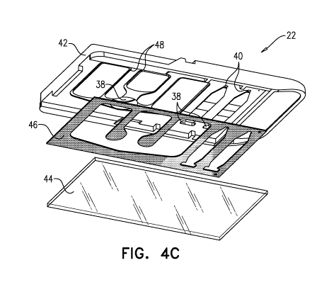
Reference is now made to Figs. 4A, 4B, 4C, and 4D, which are schematic
illustrations
of respective views of sample carrier 22, the sample carrier being configured
for facilitating
both microscopic measurements, and optical density measurements with respect
to the
sample, in accordance with some applications of the present invention. Figs.
4A shows a
top view of the sample carrier (the top cover of the sample carrier being
shown as being
opaque in Fig. 4A, for illustrative purposes), Fig. 4B shows a bottom view (in
which the
sample carrier has been rotated around its long edge with respect to the view
shown in Fig.
4A), and Fig. 4C shows an exploded side view.
For some applications, a sample carrier as shown in Figs. 4A-C is used when
performing a complete blood count on a blood sample. For some applications,
the sample
carrier includes a first set 52 of chambers, which are used for performing
microscopic
analysis upon the sample, and a second set 54 of chambers, which are used for
performing
optical density measurements upon the sample. As described hereinabove with
reference to
Figs. 2A-D, for some applications, the sample carrier is made of a molded
component 42, a
glass sheet 44 and an adhesive layer 46, as shown in Fig. 4C. For some
applications, the
adhesive layer is configured to fluoresce and/or to become photobleached, as
described
hereinabove. Typically, the molded component is configured to define inlet
holes 38, outlet
holes 40, and/or gutters 48, which are generally as described hereinabove.
As described in WO 17/195205 to Pollack, which is incorporated herein by
reference, for some applications, chambers belonging to set 54 (which is used
for optical
density measurements), typically define at least a first region 56 (which is
typically deeper)
and a second region 58 (which is typically shallower), the height of the
chambers varying
between the first and second regions in a predefined manner.
Typically, in order to perform optical analysis upon the sample, it is
desirable to
know the optical path length, the volume, and/or the thickness of the portion
of the sample
upon which the optical measurements were performed, as precisely as possible.
Further
typically, the optical measurements are performed upon a portion of the sample
disposed in
a sample carrier that is defined by two or more opposing surfaces. In order to
provide the
CA 03081669 2020-05-04
WO 2019/097387 PCT/IB2018/058861
17
desired level of precision, it is desirable for the two or more opposing
surfaces to be
separated by a distance that is correspondingly tightly set or tightly
controlled. However, in
some manufacture or assembly processes, the distance between the opposing
surfaces may
vary substantially. For example, the upper and lower surfaces of the chambers
as shown in
Figs. 4A-C are defined respectively by the molded component, and the glass
sheet, the
molded component and glass sheet being coupled to one another via the adhesive
layer.
Although the adhesive layer has a nominal thickness, it is typically the case
that, for example,
due to variation in the manufactured thickness of the pressure-sensitive
adhesive or in the
pressure applied during its application, the actual thickness of the layer is
different from the
nominal thickness. For example, molded component and the glass sheet may be
bonded
using a pressure-sensitive adhesive layer with a nominal thickness that is
configured to
separate the opposing surfaces by a separation of 100 micrometers. In such a
case, variation
in the manufactured thickness of the pressure-sensitive adhesive layer or in
the pressure
applied during its application may result in a final thickness that may lie,
for example, as far
as 20 micrometers greater or less than the nominal thickness.
Typically, an optical measurement is performed on the sample. For example, the
density of a component may be determined by performing a count of the
component within
a microscopic image. Similarly, the concentration and/or density of a
component may be
measured by performing optical absorption, transmittance, fluorescence, and/or
luminescence measurements upon the sample. Without being bound by theory, an
uncertainty of 20 percent in the distance separating the two opposing surfaces
(as described
in the above example), may, in turn, correspond to 20 percent uncertainty in
parameters of
the sample that are derived from the optical measurements that are performed
upon the
sample (such as, the derived concentration and/or density of a component
within the sample),
e.g., as described in WO 17/195205 to Pollack, which is incorporated herein by
reference.
In accordance with some applications of the present invention, the above-
described
problems associated with uncertainty relating to the height of a sample
chamber are at least
partially overcome. Referring again to Fig. 4A, sample chambers belonging to
set 54 define
first region 56 and second region 58. The heights of first region 56 and
second region 58 of
the sample chamber are defined by a lower surface that is defined by the glass
sheet and by
an upper surface that is defined by the molded component. The upper surface at
the second
region is stepped with respect to the upper surface at the first region. The
step between the
CA 03081669 2020-05-04
WO 2019/097387 PCT/IB2018/058861
18
upper surface at the first and second regions, provides a predefined height
difference Ah
between the regions, such that even if the absolute height of the regions is
not known to a
sufficient degree of accuracy, the height difference Ah is known to a
sufficient degree of
accuracy to determine a parameter of the sample, using the techniques
described herein, and
as described in WO 17/195205 to Pollack, which is incorporated herein by
reference.
As described hereinabove, the molded component is shaped to define a stepped
surface such as to define the manner in which the height of the chambers
belonging to set 54
varies between the first and second regions. Typically, relative manufacturing
tolerances
within a single substrate, and especially between nearby surfaces, are tighter
than
manufacturing tolerances on positioning between different substrates or even
between
opposing surfaces lying within the same substrate. Therefore, it is typically
the case that by
having a single substrate define the manner in which the height of the one or
more sample
chambers varies between the first and second regions, the height difference
between the first
and second regions is relatively precise. For example, the molded component
may be
manufactured with relatively tight tolerances, for example, using injection
molding,
embossing or machining.
As described with reference to WO 17/195205 to Pollack, which is incorporated
herein by reference, for some applications, chambers belonging to set 52
(which is used for
microscopy measurements) have different heights from each other, in order to
facilitate
different measurands being measured using microscope images of respective
chambers,
and/or different chambers being used for microscopic analysis of respective
sample types.
For example, if a blood sample, and/or a monolayer formed by the sample, has a
relatively
low density of red blood cells, then measurements may be performed within a
chamber of
the sample carrier having a relatively great height, such that there is a
sufficient density of
cells, and/or such that there is a sufficient density of cells within the
monolayer formed by
the sample, to provide statistically reliable data. Such measurements may
include, for
example red blood cell density measurements, measurements of other cellular
attributes,
(such as counts of abnormal red blood cells, red blood cells that include
intracellular bodies
(e.g., pathogens, Howell-Jolly bodies), etc.), and/or hemoglobin
concentration. Conversely,
if a blood sample, and/or a monolayer formed by the sample, has a relatively
high density of
red blood cells, then such measurements may be performed upon a chamber of the
sample
carrier having a relatively low height, for example, such that there is a
sufficient sparsity of
CA 03081669 2020-05-04
WO 2019/097387 PCT/IB2018/058861
19
cells, and/or such that there is a sufficient sparsity of cells within the
monolayer of cells
formed by the sample, that the cells can be identified within microscopic
images. For some
applications, such methods are performed even without the variation in height
between the
chambers belonging to set 52 being precisely known.
For some applications, based upon the measurand that is being measured, the
chamber within the sample carrier upon which to perform optical measurements
is selected.
For example, a chamber of the sample carrier having a relatively great height
may be used
to perform a white blood cell count (e.g., to reduce statistical errors which
may result from
a low count in a shallower region), white blood cell differentiation, and/or
to detect more
rare forms of white blood cells. Conversely, in order to determine mean
corpuscular
hemoglobin (MCH), mean corpuscular volume (MCV), red blood cell distribution
width
(RDW), red blood cell morphologic features, and/or red blood cell
abnormalities,
microscopic images may be obtained from a chamber of the sample chamber having
a
relatively low height, since in such chambers the cells are relatively
sparsely distributed
across the area of the region, and/or form a monolayer in which the cells are
relatively
sparsely distributed. Similarly, in order to count platelets, classify
platelets, and/or extract
any other attributes (such as volume) of platelets, microscopic images may be
obtained from
a chamber of the sample chamber having a relatively low height, since within
such chambers
there are fewer red blood cells which overlap (fully or partially) with the
platelets in
microscopic images, and/or in a monolayer.
In accordance with the above-described examples, it is preferable to use a
chamber
of the sample carrier having a lower height for performing optical
measurements for
measuring some measurands within a sample (such as a blood sample), whereas it
is
preferable to use a chamber of the sample carrier having a greater height for
performing
optical measurements for measuring other measurands within such a sample.
Therefore, for
some applications, a first measurand within a sample is measured, by
performing a first
optical measurement upon (e.g., by acquiring microscopic images of) a portion
of the sample
that is disposed within a first chamber belonging to set 52 of the sample
carrier, and a second
measurand of the same sample is measured, by performing a second optical
measurement
upon (e.g., by acquiring microscopic images of) a portion of the sample that
is disposed
within a second chamber of set 52 of the sample carrier. For some
applications, the first
CA 03081669 2020-05-04
WO 2019/097387 PCT/IB2018/058861
and second measurands are normalized with respect to each other, for example,
using
techniques as described in WO 17/195208 to Zait, which is incorporated herein
by reference.
Reference is now made to Figs. 5A, 5B, and 5C, which are schematic
illustrations of
respective views of sample carrier 22, the sample carrier being configured for
use in
5 performing both microscopic measurements, and optical density measurements,
in
accordance with some applications of the present invention. Fig. 5A shows a
bottom view
of the sample carrier, with the bottom surface being transparent, such that
features of the
chambers of the sample carrier may be observed. Figs. 5B and 5C show top views
of the
sample carrier in which the top layer of the sample carrier is opaque (and in
which the sample
10 carrier has been rotated around its long edge with respect to the view
shown in Fig. 5A).
Sample carrier as shown in Figs. 5A, 5B, and 5C is generally similar to that
shown
in Figs. 4A-C, and described with reference thereto, except for differences
described
hereinbelow. For some applications, the sample carrier includes first set 52
of chambers,
which are used for performing microscopic analysis upon the sample, and second
set 54 of
15 chambers, which are used for performing optical density measurements
upon the sample.
For some applications, the second set of chambers, which are used for
performing optical
density measurements upon the sample includes only a single chamber, as shown.
For some
applications, there is a plurality of chambers within the first set 52 of
chambers, which are
used for performing microscopic analysis upon the sample, and each of the
chambers defines
20 an outlet hole 40 (which is generally as described hereinabove). For
some such applications,
the outlet holes of each of the chambers belonging to the first set of
chambers are disposed
in close proximity to each other (as shown in Fig. 5B), e.g., such that the
holes are disposed
along a line measuring less than 1 cm long. For example, there may be
respective channels
51 leading from each of the chambers to its outlet hole, such that the outlet
holes are disposed
in close proximity to each other.
For some applications, a cover 60 (shown in Fig. 5C) is reversibly (or,
optionally,
irreversibly) coupled to the sample carrier, such as to cover the outlet
holes. For example,
the cover may include paper, sponge or filter material that has an adhesive
backing.
Typically, the cover is configured to prevent the sample from leaking out of
the sample
carrier, thereby reducing the likelihood of the optical measuring device
becoming
contaminated by leakage from the sample carrier. For some applications, the
cover is
configured to control the rate of filling of the first set 52 of chambers, by
limiting the rate of
CA 03081669 2020-05-04
WO 2019/097387 PCT/IB2018/058861
21
air flow out of the chambers. For some applications (not shown), a cover that
is generally
similar to cover 60 is placed over outlet holes associated with second set 54
of chambers.
For some applications, sample carrier 22 is shaped to define a reservoir 39
that is
adjacent to inlet hole 38. Typically, the reservoir is configured to allow the
user to fill the
chambers of the sample carrier with the bodily sample, such that, on the one
hand, the user
is not required to insert a precise volume of the bodily sample into the inlet
hole, and yet, on
the other hand, the inlet hole is left substantially free of liquids.
Reference is now made to Fig. 6 which is a schematic illustration showing a
bottom
view of sample carrier 22, a chamber of the sample carrier including a first
marking 62 on
its lower inner surface (i.e., the inner surface of the glass layer), and a
second marking 64 on
its upper inner surface (e.g., the inner surface of the substrate layer), in
accordance with
some applications of the present invention. In the view shown in Fig. 6, the
inner surface of
the substrate layer is visible through the transparent glass layer. In
accordance with
respective applications, the markings may constitute lines, or other shapes
(e.g.,
alphanumeric characters). The markings may be imprinted on the sample carrier,
drawn on
the sample carrier, etched on the sample carrier, engraved on the sample
carrier, glued on
the sample carrier, embedded within the sample carrier, may constitute
protrusions and/or
indentations within the sample carrier and/or other visible features of the
sample carrier,
and/or may be attached to the sample carrier.
Typically, a sample fills a volume having a height that is defined by the
upper and
lower surfaces. For example, the volume of a portion of the sample in one of
the chambers
is defined by the area of the chamber multiplied by the height of the chamber.
However, in
some cases, the exact height of the chamber is not known, for example, for the
reasons
provided hereinabove. For some applications, the computer processor determines
the height
of the chamber by focusing an imaging module of the optical measurement device
on first
marking 62 and registering an indication of the focusing distance Fl
associated with the first
marking. The computer processor also focuses the imaging module of the optical
measurement device on second marking 64 and registers an indication of the
focusing
distance F2 associated with the second marking. The computer processor then
determines
the height of the chamber, based upon the difference between Fl and F2. For
some
applications, the computer processor determines the volume of the chamber, or
a portion
thereof, based upon the determined height of the chamber. Typically, the
computer
CA 03081669 2020-05-04
WO 2019/097387 PCT/IB2018/058861
22
processor determines a property of the sample at least partially based upon
the determined
height of the chamber, for example, using techniques as described hereinabove.
There is typically a degree of variation in the positioning of the sample
carrier with
respect to an imaging module of optical measurement device 24. For example,
placement
of the sample carrier on a microscope stage can vary significantly in view of
the required
imaging resolution (due for example to limitations of the microscope,
variation in the sample
carrier, variations in placement by an operator of the device, etc.).
Therefore, in accordance
with some applications, the positioning of the sample carrier with respect to
an imaging
module of optical measurement device 24 is determined, in accordance with the
techniques
described herein.
For some applications, the imaging module of the optical measurement device
and a
stage upon which the sample carrier is placed are initially positioned such
that a visible mark
on the sample carrier appears within the observation field of the imaging
module. This is
followed by scanning a portion of the sample carrier surface until sufficient
information is
available to define the sample carrier's position and/or orientation at least
with respect to the
X-Y plane. (In the present application, the term Z-axis is used to refer to
the optical axis of
the optical system, and the X-Y plane is used to denote the plane that is
perpendicular to the
optical axis, as is common in the art)
Reference is now made to Figs. 7A and 7B, in which an example of an irregular
pattern 70 is shown, the pattern including a set of vertical lines 72 and
horizontal lines 74
confined within a square boundary 76, in accordance with some applications of
the present
invention. Fig. 7B shows the irregular pattern shown in Fig. 7A in an
orientation that is
tilted with respect to that shown in Fig. 7A. For some applications, an
irregular pattern, such
as that shown in Figs. 7A-B, is marked upon sample carrier 22. Optical
measurement device,
which typically includes a microscope system, images the sample carrier via an
observation
field. Typically, such observation fields image sub-portions within chambers
of the sample
carrier.
It may be observed that the spacing between the vertical lines 72 is
irregular, i.e. the
distance between each two neighboring vertical lines 72 is different than any
of two other
neighboring vertical lines 72. The same design is applied to the horizontal
lines. By way of
CA 03081669 2020-05-04
WO 2019/097387 PCT/IB2018/058861
23
example, the irregular pattern may measure about 2.7 X 2.7 mm2, while the
observation field
may measure about 0.6 X 0.8 mm2.
It is noted that while irregular pattern 70 and the observation field are
shown as being
essentially rectangular or square, any other shape may be used. For example, a
round or
other shape observation field may be selected, for example based on optical
limitations
which may provide a better image in a portion of a diagnostic field.
As described hereinabove, the optical measurement device is typically used to
capture images of the sample using an observation field O.F. (also referred
herein as an
orientation field), which has a predetermined size and shape, and through
which (when
properly place above the sample carrier) a portion of the sample carrier can
be viewed. The
irregular pattern is designed with a resolution that is complementary to the
observation field
size so that in any lateral X-Y position of the observation field over the
irregular pattern, the
portion of the irregular pattern observed through the observation field is
unique to that
specific position and detectable at the set resolution of the device.
Optionally, an observation
field may be a diagnostic field or a portion thereof. In some embodiments, an
observation
field is assembled using a plurality of adjacent diagnostic fields, such that
the combined
information from two or more diagnostic fields is used as an observation
field.
Reference is now made to Figs. 8A, 8B, 8C, and 8D, in which examples of the
pattern
corresponding to respective observation fields are shown, in accordance with
some
applications of the present invention. It may be observed that the image of
the portion of the
irregular pattern captured at different positions of the observation field is
different for each
such position. The irregular pattern is designed so that the images captured
at any two
different X-Y positions will yield different visible portions of the irregular
pattern.
It is also noted that, typically, the resolution of the irregular pattern is
designed to be
complementary to the size and shape of the observation field, such that it is
typically not the
case that the observation field is smaller than the distance between two
neighboring lines of
the pattern (either horizontal or vertical), so that an observation field
never includes a single
line, an empty space or the sole thickness of a single line. Typically, the
only exception to
this configuration is an irregular pattern designed specifically so that such
a single line,
empty space and/or sole thickness can occur in a single position of the
observation field
across the entire irregular pattern.
CA 03081669 2020-05-04
WO 2019/097387 PCT/IB2018/058861
24
Since each position of the observation field corresponds to its own unique
pattern,
the computer processor typically determines the position of the irregular
pattern with respect
to the observation field. Since the irregular pattern is fixedly associated
with the sample
carrier, the computer processor thereby determines the location, and
optionally orientation,
of the sample carrier that is imaged within the observation field.
Reference is now made to Figs. 9A, 9B, 9C, and 9D, in which some additional
examples of the pattern corresponding to respective observation fields are
shown, in
accordance with some applications of the present invention. It is noted, with
reference to
the examples shown in Figs. 9A-D, that not only the X-Y position of the
irregular pattern be
determined via the observation field, but also the orientation thereof. Thus,
for some
applications, the computer processor determines which portion of the sample
carrier is being
imaged in a given observation field, as well as the orientation of the sample
carrier within
the observation field, based upon the irregular pattern that is identified
within the observation
field.
In accordance with some applications, the irregular pattern is imprinted on
the sample
carrier, drawn on the sample carrier, etched on the sample carrier, engraved
on the sample
carrier, glued on the sample carrier, embedded within the sample carrier,
constitutes
protrusions and/or indentations within the sample carrier, and/or other
visible features of the
sample carrier, and/or is attached to the sample carrier. Typically, the
irregular pattern (e.g.,
a 2D pattern as described with reference to Figs. 7A-10C, and/or a 3D pattern
as described
with reference to Fig. 11A-11F) is formed upon the inner surface of the molded
layer of the
sample carrier. Alternatively or additionally, the irregular pattern is formed
on a surface of
the glass layer of the sample carrier. For some applications, an irregular
pattern as described
with reference to any one of Fig. 7A-12 is used on a sample carrier having
different
characteristics to the sample carriers described with reference to Figs. 2A-6.
Reference is now made to Figs. 10A, 10B and 10C, in which three additional
examples of irregular patterns are shown, in accordance with some applications
of the
present invention. The examples that are shown are as follows:
Fig. 10A - a set of concentric circles of uniquely different diameters, and
being
overlapped by a rectangular wave pattern;
CA 03081669 2020-05-04
WO 2019/097387 PCT/IB2018/058861
Fig. 10B - a set of circles of uniquely different diameters and varying line
thicknesses, and which are not concentric; and
Fig. 10C - a spiral configuration of varying line thickness.
Each of the patterns shown in Figs. 10A to 10C provides a unique image to
respective
5 observation fields that are disposed at different X-Y positions above the
irregular pattern. In
addition, each of the patterns shown in Figs. 10A to 10C provides a unique
image to
respective observation fields that are disposed at different angular
orientations above the
irregular pattern, such that it is possible to distinguish between angular
positions that are
separated by less than 5 degrees.
10 In principle, it should be appreciated that while a single irregular
pattern may be
sufficient for determining both location and orientation of the sample
carrier, the subject
matter of the present disclosure does not exclude the use of two or more such
patterns in a
single carrier/chamber, potentially allowing for more accurate results.
For some applications, the irregular pattern is a 3D pattern having elements
thereof
15 located at different heights along the Z-axis. Optionally, the maximum
height of the 3D
pattern relative to the minimum height measures about 10 iim. For some
applications, the
3D pattern is marked on a surface having the same position along the optical
axis of the
imaging module of the optical measurement device as the surface upon which the
sample is
to be imaged. For example, the 3D pattern may be located on the surface and/or
be
20 embedded within the material.
It should be noted that according to some applications, a 3D pattern is used
such that
even a single image, or no more than 10 images, are needed to provide
sufficient information
to determine the position, and optionally also orientation of the sample
carrier, with respect
to an imaging module of an optical measurement device, both with respect to an
XY plane
25 of the observation field and along the optical axis of the imaging
module.
For some applications, the 3D pattern is associated with a 2D pattern or mark
as
described above (either juxtaposed therewith or being a part thereof), so that
once
information is gathered from the 2D mark or pattern (regarding the position,
and optionally
orientation, of the sample carrier with respect to an X-Y plane of the visual
examination
zone), a single image of the 3D pattern is enough to determine the location of
the sample
carrier along the optical axis of an imaging module.
CA 03081669 2020-05-04
WO 2019/097387 PCT/IB2018/058861
26
Reference is now made to Fig. 11A in which a 3D pattern 80 is shown, in which
the
irregular pattern is reflected not only in the 2D grid design, but also in
varying depths of
different areas of the pattern, in accordance with some applications of the
present invention.
In particular, the 3D pattern is in the form of an irregular grid of
rectangular portions, each
rectangle having a top at a certain depth from the surface, such that at least
some different
rectangles have different depths.
Reference is also made to Fig. 11B, in which a portion of the 3D pattern is
shown
(e.g. a portion of the pattern observed by the observation field 0.F.),
comprising nine
rectangles sql to sq9, each rectangle being at one of four depths DO to D3, in
accordance
with some applications of the present invention. Specifically, the arrangement
shown in Fig.
11B is as follows:
Rectangle No. Depth
sql, sq3, sq8 DO
sq2, sq6 D1
sq4, sq9 D2
sq5, sq7 D3
Reference is also made to Figs. 11C to 11F, each showing an example of an
image
of the 3D portion taken by the imaging module of the optical measurement
device at depths
DO to D3 respectively, in accordance with some applications of the present
invention. It may
be observed that, at each focal length of the imaging module of the optical
measurement
device, corresponding to each of the depths DO to D3, the image received is
such that the
boundaries of the rectangles at that depth/focal length are clearly visible
(indicated by the
solid lines), while the remainder of the rectangles (which are not located at
that depth/focal
length) are not in focus (indicated by the dashed lines).
Thus, for some applications, the 3D feature of the irregular pattern is used
by
computer processor 28 to provide an additional degree of accuracy for
determining the
position of the sample carrier with respect to the imaging module of the
optical measurement
device. Alternatively or additionally, the 3D feature of the irregular pattern
is used by
computer processor 28 to provide an indication as to the focal length of the
imaging module
CA 03081669 2020-05-04
WO 2019/097387 PCT/IB2018/058861
27
of the optical measurement device. A single image taken of the 3D pattern may
provide
sufficient information regarding the position of the grid in the X-Y plane as
well as along
the optical axis of the imaging module of the optical measurement device.
Optionally, once
the X-Y position is known, an image (e.g., a single image) of the 3D pattern
is taken at the
known X-Y position, and the computer processor derives the location of the 3D
pattern along
the optical axis of the imaging module of the optical measurement device using
the image.
It should be appreciated that the depths DO to D3 are not necessarily equally
spaced,
and the height differences between respective pairs of consecutive height
levels can be
different from each other.
Reference is now made to Fig. 12, which is a schematic illustration of the
spatial
arrangement of an irregular pattern of a sample carrier with respect to an
observation field
O.F. of the imaging module of optical measurement device 24, in accordance
with some
applications of the present invention. As shown, a sample carrier may be
located in one of
a plurality of X-Y positions with respect to the observation field. In this
example, two
extreme positions, Position A and Position B, of the sample carrier with
respect to the
observation field are depicted, the positions differing in location by a
length Lx along the X-
axis, and by a length Ly along the Y-axis. The spatial arrangement of the
irregular pattern
along the carrier is typically such that at least a portion of the irregular
pattern falls within
the observation field, regardless of the relative position of the carrier with
respect to the
optical device. Thus, the position of the sample carrier with respect to the
imaging module
of the optical measurement device does not affect the optical measurement
device's ability
to operate properly.
For some applications, the sample as described herein is a sample that
includes blood
or components thereof (e.g., a diluted or non-diluted whole blood sample, a
sample including
predominantly red blood cells, or a diluted sample including predominantly red
blood cells),
and parameters are determined relating to components in the blood such as
platelets, white
blood cells, anomalous white blood cells, circulating tumor cells, red blood
cells,
reticulocytes, Howell-Jolly bodies, etc.
In general, it is noted that although some applications of the present
invention have
been described with respect to a blood sample, the scope of the present
invention includes
applying the apparatus and methods described herein to a variety of samples.
For some
CA 03081669 2020-05-04
WO 2019/097387 PCT/IB2018/058861
28
applications, the sample is a biological sample, such as, blood, saliva,
semen, sweat, sputum,
vaginal fluid, stool, breast milk, bronchoalveolar lavage, gastric lavage,
tears and/or nasal
discharge. The biological sample may be from any living creature, and is
typically from
warm blooded animals. For some applications, the biological sample is a sample
from a
mammal, e.g., from a human body. For some applications, the sample is taken
from any
domestic animal, zoo animals and farm animals, including but not limited to
dogs, cats,
horses, cows and sheep. Alternatively or additionally, the biological sample
is taken from
animals that act as disease vectors including deer or rats.
For some applications, similar techniques to those described hereinabove are
applied
to a non-bodily sample. For some applications, the sample is an environmental
sample, such
as, a water (e.g. groundwater) sample, surface swab, soil sample, air sample,
or any
combination thereof. In some embodiments, the sample is a food sample, such
as, a meat
sample, dairy sample, water sample, wash-liquid sample, beverage sample,
and/or any
combination thereof.
Applications of the invention described herein can take the form of a computer
program product accessible from a computer-usable or computer-readable medium
(e.g., a
non-transitory computer-readable medium) providing program code for use by or
in
connection with a computer or any instruction execution system, such as
computer processor
28. For the purposes of this description, a computer-usable or computer
readable medium
can be any apparatus that can comprise, store, communicate, propagate, or
transport the
program for use by or in connection with the instruction execution system,
apparatus, or
device. The medium can be an electronic, magnetic, optical, electromagnetic,
infrared, or
semiconductor system (or apparatus or device) or a propagation medium.
Typically, the
computer-usable or computer readable medium is a non-transitory computer-
usable or
computer readable medium.
Examples of a computer-readable medium include a semiconductor or solid state
memory, magnetic tape, a removable computer diskette, a random-access memory
(RAM),
a read-only memory (ROM), a rigid magnetic disk and an optical disk. Current
examples of
optical disks include compact disk-read only memory (CD-ROM), compact disk-
read/write
(CD-RAY) and DVD.
CA 03081669 2020-05-04
WO 2019/097387 PCT/IB2018/058861
29
A data processing system suitable for storing and/or executing program code
will
include at least one processor (e.g., computer processor 28) coupled directly
or indirectly to
memory elements (e.g., memory 30) through a system bus. The memory elements
can
include local memory employed during actual execution of the program code,
bulk storage,
and cache memories which provide temporary storage of at least some program
code in order
to reduce the number of times code must be retrieved from bulk storage during
execution.
The system can read the inventive instructions on the program storage devices
and follow
these instructions to execute the methodology of the embodiments of the
invention.
Network adapters may be coupled to the processor to enable the processor to
become
coupled to other processors or remote printers or storage devices through
intervening private
or public networks. Modems, cable modem and Ethernet cards are just a few of
the currently
available types of network adapters.
Computer program code for carrying out operations of the present invention may
be
written in any combination of one or more programming languages, including an
object-
oriented programming language such as Java, Smalltalk, C++ or the like and
conventional
procedural programming languages, such as the C programming language or
similar
programming languages.
It will be understood that algorithms described herein, can be implemented by
computer program instructions. These computer program instructions may be
provided to a
processor of a general-purpose computer, special purpose computer, or other
programmable
data processing apparatus to produce a machine, such that the instructions,
which execute
via the processor of the computer (e.g., computer processor 28) or other
programmable data
processing apparatus, create means for implementing the functions/acts
specified in the
algorithms described in the present application. These computer program
instructions may
also be stored in a computer-readable medium (e.g., a non-transitory computer-
readable
medium) that can direct a computer or other programmable data processing
apparatus to
function in a particular manner, such that the instructions stored in the
computer-readable
medium produce an article of manufacture including instruction means which
implement the
function/act specified in the flowchart blocks and algorithms. The computer
program
instructions may also be loaded onto a computer or other programmable data
processing
apparatus to cause a series of operational steps to be performed on the
computer or other
programmable apparatus to produce a computer implemented process such that the
CA 03081669 2020-05-04
WO 2019/097387 PCT/IB2018/058861
instructions which execute on the computer or other programmable apparatus
provide
processes for implementing the functions/acts specified in the algorithms
described in the
present application.
Computer processor 28 is typically a hardware device programmed with computer
5 program instructions to produce a special purpose computer. For example,
when
programmed to perform the algorithms described herein, computer processor 28
typically
acts as a special purpose sample-analysis computer processor. Typically, the
operations
described herein that are performed by computer processor 28 transform the
physical state
of memory 30, which is a real physical article, to have a different magnetic
polarity, electrical
10 charge, or the like depending on the technology of the memory that is
used.
There is provided, in accordance with some applications of the present
invention, the
following inventive concepts:
Inventive concept 1. Apparatus comprising:
a sample carrier configured to carry a sample; and
15 an optical measurement device configured to perform optical
measurements upon the
sample, the optical measurement device defining an observation field,
the sample carrier comprising a surface that comprises at least one irregular
pattern, such that any portion of the surface of the sample carrier having a
shape and
area that corresponds to the observation field of the optical measurement
device and
20 that contains at least a portion of the pattern has a geometric
pattern unique to that
portion.
Inventive concept 2. The apparatus according to inventive concept 1, wherein
the irregular
pattern is configured to facilitate determining a position of the sample
carrier with respect to
a plane of the observation field, based on a single image of any portion of
the surface of the
25 sample carrier that contains a portion of the pattern having a geometric
pattern unique to that
portion.
Inventive concept 3. The apparatus according to inventive concept 1, wherein
the irregular
pattern has a given orientation with respect to the surface of the sample
carrier, such that the
sample carrier facilitates determining orientation of the sample carrier with
respect to the
30 observation field of the optical measurement device
CA 03081669 2020-05-04
WO 2019/097387 PCT/IB2018/058861
31
Inventive concept 4. The apparatus according to inventive concept 1, wherein
the irregular
pattern is present on the surface of the carrier using one or more techniques
selected from
the group consisting of: drawing, embossing, etching, carving, and adhering.
Inventive concept 5. The apparatus according to inventive concept 1, wherein
the surface
of the sample carrier that comprise the irregular pattern comprises a surface
of a sample
chamber that is configured to carry the sample therein.
Inventive concept 6. The apparatus according to inventive concept 1, wherein
the carrier
comprises a cover, and wherein the surface of the sample carrier that comprise
the irregular
pattern comprises a surface of the cover.
Inventive concept 7. The apparatus according to inventive concept 1, wherein
the surface
of the sample carrier that comprise the irregular pattern comprises a surface
of the sample
carrier that is located on the sample carrier outside any chamber.
Inventive concept 8. The apparatus according to inventive concept 1, wherein
the optical
measurement device comprises a microscope.
Inventive concept 9. The apparatus according to inventive concept 1, wherein
the sample
carrier comprises two or more irregular patterns.
Inventive concept 10. The apparatus according to inventive concept 1, wherein
the said
sample carrier comprises two or more chambers, each configured to carry a
portion of the
sample therein.
Inventive concept 11. The sample carrier according to inventive concept 10,
wherein at least
one of said at least one irregular pattern is located on a surface of each of
said two or more
chambers.
Inventive concept 12. A sample carrier configured for containing a sample to
be analyzed
by an optical measurement device having a maximal visual examining zone of
area A at a
diagnostic imaging magnification, wherein the initial imaging position of the
carrier may
vary by a length L in at least one of the X and Y axis of a plane being
perpendicular to the
optic axis of the optic device and having a visual examining zone of area S,
said sample
carrier comprising at least one irregular pattern having an area A', where A'
= f (A,L); such
that any image having the same shape and area as that of the visual examining
zone taken at
CA 03081669 2020-05-04
WO 2019/097387 PCT/IB2018/058861
32
an expected initial location of the irregular pattern would comprise a portion
of the pattern
that has a geometric pattern unique to that portion.
Inventive concept 13. A sample carrier configured for containing a sample to
be analyzed
by an optical measurement device the carrier comprising at least one irregular
geometric
pattern having an area of at least 6mm2 such that any portion of the pattern
having the same
size and shape and having an area of 0.3 mm2 or more and comprising at least a
portion of
the pattern has a geometric pattern unique to that portion.
Inventive concept 14. The sample carrier of inventive concept 13, wherein an
inscribing
circle of said irregular geometric pattern measures at least 3mm in diameter,
and does not
measure less than 2mm in two perpendicular directions.
Inventive concept 15. The sample carrier of inventive concept 13, wherein the
inscribing
circle of said portion measures at least 0.5 mm in diameter, and does not
measure less than
0.4 mm in two perpendicular directions.
Inventive concept 16. An automated microscope configured to analyze a sample
within a
sample carrier comprising:
an optical module;
a support for holding a sample carrier; and
a controller configured to:
operate the optical module to capture ten orientation images or less of the
sample carrier at a predetermined location; and
analyze the images to deduce at least one of a position and orientation of the
carrier or a portion thereof with respect to at least one of an XY plane and a
z axis of
the microscope,
wherein the sample carrier comprises at least one irregular pattern and the
irregular
pattern is sized and positioned on a sample carrier surface such that at least
one of said ten
orientation images or less shows the irregular pattern or a part thereof
without searching.
Inventive concept 17. An automated microscope according to inventive concept
16, wherein
the irregular pattern is patterned such that any portion of an orientation
image that shows the
irregular pattern or a part thereof shows a geometric pattern unique to that
portion.
CA 03081669 2020-05-04
WO 2019/097387 PCT/IB2018/058861
33
Inventive concept 18. An automated microscope according to inventive concept
16, wherein
the irregular pattern is sized, shaped and positioned such that one image per
pattern is
sufficient for determining at least one of a position and orientation of the
sample carrier.
Inventive concept 19. A sample carrier for a microscope, comprising at least
one chamber
configured for containing therein a sample to be analyzed, said chamber
comprising:
a cavity with a platform disposed therein and having a platform surface
elevated
above a floor surface of the cavity; and
a cover covering said cavity spaced from said platform surface;
wherein said platform surface comprises a first mark and a said cover
comprises on
a surface thereof a second mark, wherein the focusing distance between the
first mark and
the second mark allows determining a vertical length of the space between said
platform
surface and a bottom surface of said cover.
Inventive concept 20. A sample carrier for a microscope according to inventive
concept 19,
wherein the second mark is on the bottom surface of said cover.
Inventive concept 21. A sample carrier for a microscope according to inventive
concept 19,
wherein the first mark and second mark overlap along the Z axis.
Inventive concept 22. A sample carrier for a microscope according to inventive
concept 19,
wherein at least one of the first mark and second mark comprises an irregular
pattern.
Inventive concept 23. A method for determining a volume of a portion of a
fluid sample in
a sample carrier of inventive concept 19, comprising:
introducing the fluid sample into said sample carrier such that the sample
fills a
volume having a height defined between said platform surface and a bottom
surface of said
cover;
determining an area A of a portion of said platform surface;
focusing an optical module of the microscope on said first mark and
registering an
indication of the focusing distance Fi for said first mark;
focusing an optical module of the microscope on said second mark and
registering
an indication of the focusing distance F2 for said second mark; and
determining based on Fl, F2 and A, a volume of the fluid sample located on
said
portion of the platform surface.
CA 03081669 2020-05-04
WO 2019/097387 PCT/IB2018/058861
34
The apparatus and methods described herein may be used in conjunction with
apparatus and methods described in any one of the following patent
applications, all of which
are incorporated herein by reference:
US 2012/0169863 to Bachelet;
US 2014/0347459 to Greenfield;
US 2015/0037806 to Pollak;
US 2015/0316477 to Pollak;
US 2016/0208306 to Pollak;
US 2016/0246046 to Yorav Raphael;
US 2016/0279633 to Bachelet;
US 2018/0246313 to Eshel;
WO 16/030897 to Yorav Raphael;
WO 17/046799 to Eshel;
WO 17/168411 to Eshel;
WO 17/195205 to Pollack; and
WO 17/195208 to Zait.
It will be appreciated by persons skilled in the art that the present
invention is not
limited to what has been particularly shown and described hereinabove. Rather,
the scope
of the present invention includes both combinations and subcombinations of the
various
features described hereinabove, as well as variations and modifications
thereof that are not
in the prior art, which would occur to persons skilled in the art upon reading
the foregoing
description.