Note: Descriptions are shown in the official language in which they were submitted.
NON-INVASIVE NERVE ACTIVATOR WITH ADAPTIVE CIRCUIT
CROSS REFERENCE TO RELATED APPLICATIONS
[0001]This application claims priority to U.S. Provisional Patent Application
Serial No. 62/582,634, filed on November 7, 2017, and to U.S. Provisional
Patent
Application Serial No. 62/661,256, filed on April 23, 2018.
TECHNICAL FIELD
[0002]This invention pertains to the activation of nerves by topical
stimulators to
control or influence muscles, tissues, organs, or sensation, including pain,
in mammals,
including humans.
BACKGROUND
[0003] Nerve disorders may result in loss of control of muscle and other body
functions, loss of sensation, or pain. Surgical procedures and medications
sometimes
treat these disorders but have limitations. This invention pertains to a
system for
offering other options for treatment and improvement of function.
SUMMARY
[0004] In accordance with the invention, there is provided a topical nerve
activation patch comprising: a flexible substrate; a dermis conforming bottom
surface of
the substrate comprising adhesive and adapted to contact a derm is of a user;
a flexible
top outer surface of the substrate; a plurality of electrodes positioned on
the patch and
located beneath the top outer surface and coupled to the flexible substrate; a
power
source; and electronic circuitry embedded in the patch and located beneath the
top
outer surface and coupled to the flexible substrate, the electronic circuitry
configured to
generate an output voltage applied to the electrodes for a nerve activation
treatment,
the electronic circuitry comprising: a controller; a voltage monitoring
circuit coupled to
the controller; a current monitoring circuit coupled to the controller; a
switch coupled to
the controller; a boosted voltage circuit coupled to the switch and the power
source; and
- 1 -
Date Recue/Date Received 2022-02-11
a charge measurement circuit coupled to the controller; the electronic
circuity configured
to measure a level of charge delivered to the user when the output voltage is
applied to
the electrodes, and adjust an amount of output voltage based on the measured
level of
charge.
BRIEF DESCRIPTION OF THE DRAWINGS
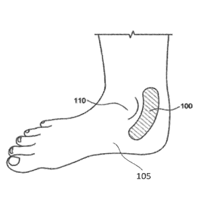
[0005] Fig. 1 illustrates an example patch that is affixed to a location
behind an
ankle bone of a user.
[0006] Fig. 2 is a block diagram illustrating hardware/software related
elements of
an example of the patch of Fig. 1.
[0007] Fig. 3A is a circuit diagram of an example of a boosted voltage circuit
that
provides feedback.
[0008] Fig. 3B is a circuit diagram of an example of a charge application
circuit
that uses an output of the boosted voltage circuit.
[0009] Fig. 4 is a flow diagram of the functionality of the controller of
monitoring
and controlling the output voltage, including its ramp rate.
[0010] Fig. 5 is a flow diagram in accordance with one example of an adaptive
protocol.
[0011] Fig. 6 is a Differential Integrator Circuit used in the adaptive
protocol in
accordance with one example.
[0012] Fig. 7 is a table relating charge duration vs. frequency to provide
feedback
to the adaptive protocol in accordance with one example.
DETAILED DESCRIPTION
[0013] A non-invasive nerve activator in accordance with various examples
disclosed herein includes novel circuitry to adequately boost voltage to a
required level
and to maintain a substantially constant level of charge for nerve activation.
Further, a
feedback loop provides for an automatic determination and adaptation of the
applied
charge level.
[0014] Fig. 1 illustrates an example patch 100, also referred to as a smart
band
aid or smartpad or Topical Nerve Activator ("TNA") or topical nerve activation
patch, that
- 2 -
Date Recue/Date Received 2022-02-11
is affixed to a location behind an ankle bone 110 of a user 105. In the
example of Fig.
1, patch 100 is adapted to activate/stimulate the tibial nerve of user 105. In
other
examples, patch 100 is worn at different locations of user 105 to activate the
tibial nerve
from a different location, or to activate a different nerve of user 105.
[0015] Patch 100 is used to stimulate these nerves and is convenient,
unobtrusive, self-powered, and may be controlled from a smartphone or other
control
device. This has the advantage of being non-invasive, controlled by consumers
themselves, and potentially distributed over the counter without a
prescription. Patch
100 provides a means of stimulating nerves without penetrating the dermis, and
can be
applied to the surface of the derm is at a location appropriate for the nerves
of interest.
In examples, patch 100 is applied by the user and is disposable.
[0016] Patch 100 in examples can be any type of device that can be fixedly
attached to a user, using adhesive in some examples, and includes a
processor/controller and instructions that are executed by the processor, or a
hardware
implementation without software instructions, as well as electrodes that apply
an
electrical stimulation to the surface of the user's skin, and associated
electrical circuitry.
Patch 100 in one example provides topical nerve activation/stimulation on the
user to
provide benefits to the user, including bladder management for an overactive
bladder
("OAB").
[0017] Patch 100 in one example can include a flexible substrate, a malleable
derm is conforming bottom surface of the substrate including adhesive and
adapted to
contact the derm is, a flexible top outer surface of the substrate
approximately parallel to
the bottom surface, one or more electrodes positioned on the patch proximal to
the
bottom surface and located beneath the top outer surface and directly
contacting the
flexible substrate, electronic circuitry (as disclosed herein) embedded in the
patch and
located beneath the top outer surface and integrated as a system on a chip
that is
directly contacting the flexible substrate, the electronic circuitry
integrated as a system
on a chip and including an electrical signal generator integral to the
malleable derm is
conforming bottom surface configured to electrically activate the one or more
electrodes, a signal activator coupled to the electrical signal generator, a
nerve
stimulation sensor that provides feedback in response to a stimulation of one
or more
- 3 -
Date Recue/Date Received 2022-02-11
nerves, an antenna configured to communicate with a remote activation device,
a power
source in electrical communication with the electrical signal generator, and
the signal
activator, where the signal activator is configured to activate in response to
receipt of a
communication with the activation device by the antenna and the electrical
signal
generator configured to generate one or more electrical stimuli in response to
activation
by the signal activator, and the electrical stimuli configured to stimulate
one or more
nerves of a user wearing patch 100 at least at one location proximate to patch
100.
Additional details of examples of patch 100 beyond the novel details disclosed
herein
are disclosed in U.S. Pat. No. 10,016,600, entitled "Topical Neurological
Stimulation".
[0018] Fig. 2 is a block diagram illustrating hardware/software related
elements of
an example of patch 100 of Fig. 1. Patch 100 includes electronic circuits or
chips 1000
that perform the functions of: communications with an external control device,
such as
a smartphone or fob, or external processing such as cloud based processing
devices,
nerve activation via electrodes 1008 that produce a wide range of electric
fields
according to a treatment regimen, and a wide range of sensors 1006 such as,
but not
limited to, mechanical motion and pressure, temperature, humidity, acoustic,
chemical
and positioning sensors. In another example, patch 100 includes transducers
1014 to
transmit signals to the tissue or to receive signals from the tissue.
[0019] One arrangement is to integrate a wide variety of these functions into
a
system on a chip 1000. Within this is shown a control unit 1002 for data
processing,
communications, transducer interface and storage, and one or more stimulators
1004
and sensors 1006 that are connected to electrodes 1008. Control unit 1002 can
be
implemented by a general purpose processor/controller, or a specific purpose
processor/controller, or a special purpose logical circuit. An antenna 1010 is
incorporated for external communications by control unit 1002. Also included
is an
internal power supply 1012, which may be, for example, a battery. Other
examples may
include an external power supply. It may be necessary to include more than one
chip to
accommodate a wide range of voltages for data processing and stimulation.
Electronic
circuits and chips will communicate with each other via conductive tracks
within the
device capable of transferring data and/or power.
[0020] Patch 100 interprets a data stream from control unit 1002 to separate
out
- 4 -
Date Recue/Date Received 2022-02-11
message headers and delimiters from control instructions. In one example,
control
instructions include information such as voltage level and pulse pattern.
Patch 100
activates stimulator 1004 to generate a stimulation signal to electrodes 1008
placed on
the tissue according to the control instructions. In another example, patch
100 activates
transducer 1014 to send a signal to the tissue. In another example, control
instructions
cause information such as voltage level and a pulse pattern to be retrieved
from a
library stored by patch 100, such as storage within control unit 1002.
[0021] Patch 100 receives sensory signals from the tissue and translates them
to
a data stream that is recognized by control unit 1002. Sensory signals can
include
electrical, mechanical, acoustic, optical and chemical signals. Sensory
signals are
received by patch 100 through electrodes 1008 or from other inputs originating
from
mechanical, acoustic, optical, or chemical transducers. For example, an
electrical
signal from the tissue is introduced to patch 100 through electrodes 1008, is
converted
from an analog signal to a digital signal and then inserted into a data stream
that is sent
through antenna 1010 to the external control device. In another example an
acoustic
signal is received by transducer 1014, converted from an analog signal to a
digital
signal and then inserted into a data stream that is sent through the antenna
1010 to the
external control device. In some examples, sensory signals from the tissue are
directly
interfaced to the external control device for processing.
[0022] In examples of patch 100 disclosed above, when being used for
therapeutic treatment such as bladder management for OAB, there is a need to
control
the voltage by boosting the voltage to a selected level and providing the same
level of
charge upon activation to a mammalian nerve. Further, there is a need to
conserve
battery life by selectively using battery power. Further, there is a need to
create a
compact electronics package to facilitate mounting the electronics package on
a
relatively small mammalian dermal patch in the range of the size of an
ordinary band
aid.
[0023] To meet the above needs, examples implement a novel boosted voltage
circuit that includes a feedback circuit and a charge application circuit.
Fig. 3A is a
circuit diagram of an example of the boosted voltage circuit 200 that provides
feedback.
Fig. 3B is a circuit diagram of an example of a charge application circuit 300
that uses
- 5 -
Date Recue/Date Received 2022-02-11
an output of boosted voltage circuit 200. Boosted voltage circuit 200 includes
both
electrical components and a controller/processor 270 that includes a sequence
of
instructions that together modify the voltage level of activation/stimulation
delivered to
the external dermis of user 105 by patch 100 through electrodes.
Controller/processor
270 in examples implements control unit 1002 of Fig. 2.
[0024] Boosted voltage circuit 200 can replace an independent analog-
controlled
boost regulator by using a digital control loop to create a regulated voltage,
output
voltage 250, from the battery source. Output voltage 250 is provided as an
input
voltage to charge application circuit 300. In examples, this voltage provides
nerve
stimulation currents through the dermis/skin to deliver therapy for an
overactive bladder.
Output voltage 250, or "VBoost", at voltage output node 250, uses two digital
feedback
paths 220, 230, through controller 270. In each of these paths, controller 270
uses
sequences of instructions to interpret the measured voltages at voltage
monitor 226, or
"VADc" and current monitor 234, or "IADc", and determines the proper output
control for
accurate and stable output voltage 250.
[0025] Boosted voltage circuit 200 includes an inductor 212, a diode 214, a
capacitor 216 that together implement a boosted converter circuit 210. A
voltage
monitoring circuit 220 includes a resistor divider formed by a top resistor
222, or "RT", a
bottom resistor 224, or "RB" and voltage monitor 226. A current monitoring
circuit 230
includes a current measuring resistor 232, or "Ri" and current monitor 234. A
pulse
width modulation ("PWM") circuit 240 includes a field-effect transistor
("FET") switch
242, and a PWM driver 244. Output voltage 250 functions as a sink for the
electrical
energy. An input voltage 260, or "VBAT", is the source for the electrical
energy, and can
be implemented by power 1012 of Fig. 2.
[0026] PWM circuit 240 alters the "on" time within a digital square wave,
fixed
frequency signal to change the ratio of time that a power switch is commanded
to be
"on" versus "off." In boosted voltage circuit 200, PWM driver 244 drives FET
switch 242
to "on" and "off" states.
[0027] In operation, when FET switch 242 is on, i.e., conducting, the drain of
FET
switch 242 is brought down to Ground/GND or ground node 270. FET switch 242
remains on until its current reaches a level selected by controller 270 acting
as a servo
- 6 -
Date Recue/Date Received 2022-02-11
controller. This current is measured as a representative voltage on current
measuring
resistor 232 detected by current monitor 234. Due to the inductance of
inductor 212,
energy is stored in the magnetic field within inductor 212. The current flows
through
current measuring resistor 232 to ground until FET switch 242 is opened by PWM
driver
244.
[0028] When the intended pulse width duration is achieved, controller 270
turns
off FET switch 242. The current in inductor 212 reroutes from FET switch 242
to diode
214, causing diode 214 to forward current. Diode 214 charges capacitor 216.
Therefore, the voltage level at capacitor 216 is controlled by controller 270.
[0029] Output voltage 250 is controlled using an outer servo loop of voltage
monitor 226 and controller 270. Output voltage 250 is measured by the resistor
divider
using top resistor 222, bottom resistor 224, and voltage monitor 226. The
values of top
resistor 222 and bottom resistor 224 are selected to keep the voltage across
bottom
resistor 224 within the monitoring range of voltage monitor 226. Controller
270 monitors
the output value from voltage monitor 226.
[0030] Charge application circuit 300 includes a pulse application circuit 310
that
includes an enable switch 314. Controller 270 does not allow enable switch 314
to turn
on unless output voltage 250 is within a desired upper and lower range of the
desired
value of output voltage 250. Pulse application circuit 310 is operated by
controller 270
by asserting an enable signal 312, or "VSW", which turns on enable switch 314
to pass
the electrical energy represented by output voltage 250 through electrodes
320. At the
same time, controller 270 continues to monitor output voltage 250 and controls
PWM
driver 244 to switch FET switch 242 on and off and to maintain capacitor 216
to the
desired value of output voltage 250.
[0031] The stability of output voltage 250 can be increased by an optional
inner
feedback loop through FET Switch 242, current measuring resistor 232, and
current
monitor 234. Controller 270 monitors the output value from current monitor 234
at a
faster rate than the monitoring on voltage monitor 226 so that the variations
in the
voltages achieved at the cathode of diode 214 are minimized, thereby improving
control
of the voltage swing and load sensitivity of output voltage 250.
[0032] In one example, a voltage doubler circuit is added to boosted voltage
- 7 -
Date Recue/Date Received 2022-02-11
circuit 200 to double the high voltage output or to reduce voltage stress on
FET 242.
The voltage doubler circuit builds charge in a transfer capacitor when FET 242
is turned
on and adds voltage to the output of boosted voltage circuit 200 when FET 242
is
turned off.
[0033] As described, in examples, controller 270 uses multiple feedback loops
to
adjust the duty cycle of PWM driver 244 to create a stable output voltage 250
across a
range of values. Controller 270 uses multiple feedback loops and monitoring
circuit
parameters to control output voltage 250 and to evaluate a proper function of
the
hardware. Controller 270 acts on the feedback and monitoring values in order
to
provide improved patient safety and reduced electrical hazard by disabling
incorrect
electrical functions.
[0034] In some examples, controller 270 implements the monitoring instructions
in firmware or software code. In some examples, controller 270 implements the
monitoring instructions in a hardware state machine.
[0035] In some examples, voltage monitor 226 is an internal feature of
controller
270. In some examples, voltage monitor 226 is an external component, which
delivers
its digital output value to a digital input port of controller 270.
[0036] In some examples, current monitor 234 is an internal feature of
controller
270. In some examples, current monitor 234 is an external component, which
delivers
its digital output value to a digital input port of controller 270.
[0037] An advantage of boosted voltage circuit 200 over known circuits is
decreased component count which may result in reduced costs, reduced circuit
board
size and higher reliability. Further, booted voltage circuit 200 provides for
centralized
processing of all feedback data which leads to faster response to
malfunctions. Further,
boosted voltage circuit 200 controls outflow current from VBAT 260, which
increases the
battery's lifetime and reliability.
[0038] Fig. 4 is a flow diagram of the functionality of controller 270 of
monitoring
and controlling output voltage 250, including its ramp rate. In one example,
the
functionality of the flow diagram of Fig. 4, and Fig. 5 below, is implemented
by software
stored in memory or other computer readable or tangible medium, and executed
by a
processor. In other examples, the functionality may be performed by hardware
(e.g.,
- 8 -
Date Recue/Date Received 2022-02-11
through the use of an application-specific integrated circuit ("ASIC"), a
programmable
gate array ("PGA"), a field programmable gate array ("FPGA"), etc.), or any
combination
of hardware and software.
[0039]The pulse width modulation of FET switch 242 is controlled by one or
more pulses for which the setting of each pulse width allows more or less
charge to
accumulate as a voltage at capacitor 216 through diode 214. This pulse width
setting is
referred to as the ramp strength and it is initialized at 410. Controller 270
enables each
pulse group in sequence with a pre-determined pulse width, one stage at a
time, using a
stage index that is initialized at 412. The desired ramp strength is converted
to a pulse
width at 424, which enables and disables FET switch 242 according to the pulse
width.
During the intervals when FET switch 242 is "on", the current is measured by
current
monitor 234 at 430 and checked against the expected value at 436. When the
current
reaches the expected value, the stage is complete and the stage index is
incremented
at 440. If the desired number of stages have been applied 442, then the
functionality is
complete. Otherwise, the functionality continues to the next stage at 420.
[0040]As a result of the functionality of Fig. 4, VBAT 260 used in patch 100
operates for longer periods as the current drawn from the battery ramps at a
low rate of
increase to reduce the peak current needed to achieve the final voltage level
250 for
each activation/stimulation treatment. PWM 244 duty cycle is adjusted by
controller 270
to change the ramp strength at 410 to improve the useful life of the battery.
[0041]An open loop protocol to control current to electrodes in known neural
stimulation devices does not have feedback controls. It commands a voltage to
be set,
but does not check the actual current delivered. A stimulation pulse is sent
based on
preset parameters and cannot be modified based on feedback from the patient's
anatomy. When the device is removed and repositioned, the electrode placement
varies. Also the humidity and temperature of the anatomy changes throughout
the day.
All these factors affect the actual charge delivery if the voltage is preset.
Charge
control is a patient safety feature and facilitates an improvement in patient
comfort,
treatment consistency and efficacy of treatment.
[0042] In contrast, examples of patch 100 includes features that address these
shortcomings using controller 270 to regulate the charge applied by electrodes
320.
- 9 -
Date Recue/Date Received 2022-02-11
Controller 270 samples the voltage of the stimulation waveform, providing
feedback
and impedance calculations for an adaptive protocol to modify the stimulation
waveform in real time. The current delivered to the anatomy by the stimulation
waveform is integrated using a differential integrator and sampled and then
summed to
determine the actual charge delivered to the user for a treatment, such as OAB
treatment. After every pulse in a stimulation event, this data is analyzed and
used to
modify, in real time, subsequent pulses.
[0043] This hardware adaptation allows a firmware protocol to implement the
adaptive protocol. This protocol regulates the charge applied to the body by
changing
output voltage ("VBoosT") 250. A treatment is performed by a sequence of
periodic
pulses, which deliver charge into the body through electrodes 320. Some of the
parameters of the treatment are fixed and some are user adjustable. The
strength,
duration and frequency may be user adjustable. The user may adjust these
parameters as necessary for comfort and efficacy. The strength may be lowered
if
there is discomfort and raised if nothing is felt. The duration can be
increased if the
maximum acceptable strength results in an ineffective treatment.
[0044] A flow diagram in accordance with one example of the adaptive protocol
disclosed above is shown in Fig. 5. The adaptive protocol strives to
repeatedly and
reliably deliver a target charge ("Qtarget") during a treatment and to account
for any
environmental changes. Therefore, the functionality of Fig. 5 is to adjust the
charge
level applied to a user based on feedback, rather than use a constant level.
[0045] The mathematical expression of this protocol is as follows:
Qtarget = Qtarget (A * dS + B * dT), where A is the Strength Coefficient ¨
determined
empirically, dS is the user change in Strength, B is the Duration Coefficient
¨
determined empirically, and dT is the user change in Duration.
[0046] The adaptive protocol includes two phases in one example: Acquisition
phase 500 and Reproduction phase 520. Any change in user parameters places the
adaptive protocol in the Acquisition phase. When the first treatment is
started, a new
baseline charge is computed based on the new parameters. At a new acquisition
phase at 502, all data from the previous charge application is discarded. In
one
example, 502 indicates the first time for the current usage where the user
places patch
- 10 -
Date Recue/Date Received 2022-02-11
100 on a portion of the body and manually adjusts the charge level, which is a
series of
charge pulses, until it feels suitable, or any time the charge level is
changed, either
manually or automatically. The treatment then starts. The mathematical
expression of
this function of the application of a charge is as follows:
T* f
The charge delivered in a treatment is n
-.target = Qpulse (i)
i=1
Where T is the duration; f is the frequency of "Rep Rate"; Qpuise (i) is the
measured
charge delivered by Pulse (i) in the treatment pulse train provided as a
voltage
MON CURRENT that is the result of a Differential Integrator circuit shown in
Fig. 6
(i.e., the average amount of charge per pulse). Differential Integrator
circuit 700 of Fig.
6 is an example of a circuit used to integrate current measured over time and
quantify
the delivered charge and therefore determine the charge output over a
treatment pulse.
The number of pulses in the treatment is T *f.
[0047]As shown in of Fig. 6, MON_CURRENT 760 is the result of the
Differential Integrator Circuit 700. The Analog to Digital Conversion ("ADC")
710
feature is used to quantify voltage into a number representing the delivered
charge.
The voltage is measured between Electrode A 720 and Electrode B 730, using a
Kelvin
Connection 740. Electrode A 720 and Electrode B 730 are connected to a header
750.
A reference voltage, VREF 770, is included to keep the measurement in range.
[0048]In some examples, Analog to Digital Conversion 710 is an internal
feature
of controller 270. In some examples, Analog to Digital Conversion 710 is an
external
component, which delivers its digital output value to a digital input port on
Controller
270.
[0049]At 504 and 506, every pulse is sampled. In one example, the
functionality
of 504 and 506 lasts for 10 seconds with a pulse rate of 20 Hz, which can be
considered a full treatment cycle. The result of Acquisition phase 500 is the
target
pulse charge of n ¨target.
[0050] Fig. 7 is a table in accordance with one example showing the number of
pulses per treatment measured against two parameters, frequency and duration.
-11 -
Date Recue/Date Received 2022-02-11
Frequency is shown on the Y-axis and duration on the X-axis. The adaptive
protocol in
general performs better when using more pulses. One example uses a minimum of
100 pulses to provide for solid convergence of charge data feedback, although
a less
number of pulses can be used in other examples. Referring to the Fig. 7, a
frequency
setting of 20Hz and duration of 10 seconds produces 200 pulses.
[0051]The reproduction phase 520 begins in one example when the user
initiates another subsequent treatment after acquisition phase 500 and the
resulting
acquisition of the baseline charge, Qtarget.
For example, a full treatment cycle, as
discussed above, may take 10 seconds. After, for example, a two-hour pause as
shown at wait period 522, the user may then initiate another treatment. During
this
phase, the adaptive protocol attempts to deliver Qtarget for each subsequent
treatment.
The functionality of reproduction phase 520 is needed because, during the wait
period
522, conditions such as the impedance of the user's body due to sweat or air
humidity
may have changed. The differential integrator is sampled at the end of each
Pulse in
the Treatment. At that point, the next treatment is started and the
differential integrator
is sampled for each pulse at 524 for purposes of comparison to the acquisition
phase
Qtarget. Sampling the pulse includes measuring the output of the pulse in
terms of total
electric charge. The output of the integrator of Fig. 6 in voltage, referred
to as
Mon_Current 760, is a direct linear relationship to the delivered charge and
provides a
reading of how much charge is leaving the device and entering the user. At
526, each
single pulse is compared to the charge value determined in Acquisition phase
500 (i.e.,
the target charge) and the next pulse will be adjusted in the direction of the
difference.
NUM PULSES = (T1)
After each pulse, the observed charge, Qpulse(i), is compared to the expected
charge
per pulse.
Qpulse(i) > Qtarget/ NUM_PULSES ?
The output charge or "VBoosT" is then modified at either 528 (decreasing) or
530
(increasing) for the subsequent pulse by:
dV(i) = Gro L ¨target INUM_PULSES- Qpulse(i)]
where G is the Voltage adjustment Coefficient ¨ determined empirically. The
process
continues until the last pulse at 532.
- 12 -
Date Recue/Date Received 2022-02-11
[0052] A safety feature assures that the VBOOST will never be adjusted higher
by more than 10%. If more charge is necessary, then the repetition rate or
duration
can be increased.
[0053] In one example a boosted voltage circuit uses dedicated circuits to
servo
the boosted voltage. These circuits process voltage and/or current
measurements to
control the PWM duty cycle of the boosted voltage circuit's switch. The system
controller can set the voltage by adjusting the gain of the feedback loop in
the boosted
voltage circuit. This is done with a digital potentiometer or other digital to
analog circuit.
[0054] In one example, in general, the current is sampled for every pulse
during
acquisition phase 500 to establish target charge for reproduction. The voltage
is then
adjusted via a digital potentiometer, herein referred to as "Pot", during
reproduction
phase 520 to achieve the established target_charge.
[0055] The digital Pot is calibrated with the actual voltage at startup. A
table is
generated with sampled voltage for each wiper value. Tables are also
precomputed
storing the Pot wiper increment needed for 1v and 5v output delta at each pot
level.
This enables quick reference for voltage adjustments during the reproduction
phase.
The tables may need periodic recalibration due to battery level.
[0056] In one example, during acquisition phase 500, the data set = 100 pulses
and every pulse is sampled and the average is used as the target_charge for
reproduction phase 520. In general, fewer pulses provide a weaker data sample
to use
as a basis for reproduction phase 520.
[0057] In one example, during acquisition phase 500, the maximum data set =
1000 pulses. The maximum is used to avoid overflow of 32bit integers in
accumulating
the sum of samples. Further, 1000 pulses in one example is a sufficiently
large data
set and collecting more is likely unnecessary.
[0058] After 1000 pulses for the above example, the target_charge is computed.
Additional pulses beyond 1000 in the acquisition phase do not contribute to
the
computation of the target charge. In other examples, the maximum data set is
greater
than 1000 pulses when longer treatment cycle times are desired.
[0059] In one example, the first 3-4 pulses are generally higher than the rest
so
these are not used in acquisition phase 500. This is also accounted for in
reproduction
- 13 -
Date Recue/Date Received 2022-02-11
phase 520. Using these too high values can result in target charge being set
too high
and over stimulating on the subsequent treatments in reproduction phase 520.
In other
examples, more advanced averaging algorithms could be applied to eliminate
high and
low values.
[0060] In an example, there may be a safety concern about automatically
increasing the voltage. For example, if there is poor connection between the
device
and the user's skin, the voltage may auto-adjust at 530 up to the max. The
impedance
may then be reduced, for example by the user pressing the device firmly, which
may
result in a sudden high current. Therefore, in one example, if the sample is
500mv or
more higher than the target, it immediately adjusts to the minimum voltage.
This
example then remains in reproduction phase 520 and should adjust back to the
target
current/charge level. In another example, the maximum voltage increase is set
for a
single treatment (e.g., 10y). More than that is not needed to achieve the
established
target_charge. In another example, a max is set for VBOOST (e.g., 80V).
[0061] In various examples, it is desired to have stability during
reproduction
phase 520. In one example, this is accomplished by adjusting the voltage by
steps.
However, a relatively large step adjustment can result in oscillation or over
stimulation.
Therefore, voltage adjustments may be made in smaller steps. The step size may
be
based on both the delta between the target and sample current as well as on
the actual
VBOOST voltage level. This facilitates a quick and stable/smooth convergence
to the
target charge and uses a more gradual adjustments at lower voltages for more
sensitive users.
[0062] The following are the conditions that may be evaluated to determine the
adjustment step.
delta-mon_current = abs(sample_mon_current - target_charge)
If delta_mon_current > 500mv and VBOOST > 20V then step = 5V for increase
adjustments
(For decrease adjustments a 500mv delta triggers emergency decrease to
minimum Voltage)
If delta_mon_current > 200mv then step=1V
- 14 -
Date Recue/Date Received 2022-02-11
If delta_mon_current > 100mv and delta_mon_current > 5% *
sample_mon_current then step = 1V
[0063] In other examples, new treatments are started with voltage lower than
target voltage with a voltage buffer of approximately 10%. The impedance is
unknown
at the treatment start. These examples save the target_voltage in use at the
end of a
treatment. If the user has not adjusted the strength parameter manually, it
starts a new
treatment with saved target_voltage with the 10% buffer. This achieves target
current
quickly with the 10% buffer to avoid possible over stimulation in case
impedance has
been reduced. This also compensates for the first 3-4 pulses that are
generally higher.
[0064] As disclosed, examples apply an initial charge level, and then
automatically adjust based on feedback of the amount of current being applied.
The
charge amount can be varied up or down while being applied. Therefore, rather
than
setting and then applying a fixed voltage level throughout a treatment cycle,
implementations of the invention measure the amount of charge that is being
input to
the user, and adjust accordingly throughout the treatment to maintain a target
charge
level that is suitable for the current environment.
[0065] The Adaptive Circuit described above provides the means to monitor the
charge sent through the electrodes to the user's tissue and to adjust the
strength and
duration of sending charge so as to adapt to changes in the impedance through
the
electrode-to-skin interface and through the user's tissue such that the field
strength at
the target nerve is within the bounds needed to overcome the action potential
of that
nerve at that location and activate a nerve impulse. These changes in
impedance may
be caused by environmental changes, such as wetness or dryness of the skin or
underlying tissue, or by applied lotion or the like; or by tissue changes,
such as skin
dryness; or by changes in the device's placement on the user's skin, such as
by
removing the patch and re-applying it in a different location or orientation
relative to the
target nerve; or by combinations of the above and other factors.
[0066] The combined circuits and circuit controls disclose herein generate a
charge that is repeated on subsequent uses. The voltage boost conserves
battery
power by generating voltage on demand. The result is an effective and compact
electronics package suitable for mounting on or in a fabric or similar
material for
- 15 -
Date Recue/Date Received 2022-02-11
adherence to a dermis that allows electrodes to be placed near selected nerves
to be
activated.
[0067] Several examples are specifically illustrated and/or described herein.
However, it will be appreciated that modifications and variations of the
disclosed
examples are covered by the above teachings and within the purview of the
appended
claims without departing from the spirit and intended scope of the invention.
- 16 -
Date Recue/Date Received 2022-02-11