Note: Descriptions are shown in the official language in which they were submitted.
CA 03082624 2020-05-13
WO 2019/136024 PCT/US2018/068184
1
IMPEDANCE MATCHING CONDUCTIVE STRUCTURE FOR HIGH EFFICIENCY
RF CIRCUITS
TECHNICAL FIELD OF THE INVENTION
The present invention relates to creating impedance matching between RF
devices on the
same substrate.
BACKGROUND OF THE INVENTION
Without limiting the scope of the invention, its background is described in
connection with
impedance matching.
One such example is taught in U.S. Patent No. 9,819,991, issued to
Rajagopalan, et al.,
entitled "Adaptive impedance matching interface". These inventors are said to
teach a
device that includes a data interface connector, an application processor, and
interface
circuitry. Interface circuitry is said to be coupled between the application
processor and the
data interface connector, in which the data interface circuitry determines a
change in a signal
property of one of the signals, the change being caused by an impedance
mismatch between
the data interface connector and a media consumption device. The application
processor is
said to adjust the signal property of a subsequent one of the signals, in
response to the signal
property setting from the interface circuitry, to obtain an adjusted signal,
or can send the
adjusted signal to the media consumption device.
Another such example is taught in U.S. Patent No. 9,755,305, issued to
Desclos, et al., and
entitled "Active antenna adapted for impedance matching and band switching
using a shared
component". Briefly, these inventors are said to teach an active antenna and
associated
circuit topology that is adapted to provide active impedance matching and band
switching of
the antenna using a shared tunable component, e.g., using a shared tunable
component, such
as a tunable capacitor or other tunable component. The antenna is said to
provide a low cost
and effective active antenna solution, e.g., one or more passive components
can be further
utilized to design band switching of the antenna from a first frequency to a
second desired
frequency.
However, despite these advances, a need remains for impedance matching between
RF
devices on the same substrate.
2
SUMMARY OF THE INVENTION
In accordance with an aspect of at least one embodiment, there is provided a
method of
making an RF impedance matching device between two RF devices on a single
substrate comprising: providing a single photosensitive glass substrate
comprising
silica, lithium oxide, aluminum oxide, and cerium oxide, wherein a first RF
device and
a second RF device are formed on or in the photosensitive glass substrate;
masking a
design layout comprising one or more structures to form one or more triangular
or
trapezoidal vias on the photosensitive glass substrate; exposing at least one
portion of
the photosensitive glass substrate to an activating energy source; heating the
photosensitive glass substrate above its glass transition temperature for at
least ten
minutes; cooling the photosensitive glass substrate to transform at least part
of the
exposed glass to a crystalline material to form a glass-crystalline substrate;
etching the
glass-crystalline substrate with an etchant solution to form the one or more
triangular
or trapezoidal vias; filling the one or more triangular or trapezoidal vias
with a non-
conductive medium having a dielectric constant that is different from a
dielectric
constant from the photosensitive glass substrate; forming one or more
conductive
structures to traverse the one or more triangular or trapezoidal vias, wherein
the one or
more conductive structure are configured to be connected to the first RF
device and to
the second RF device.
In accordance with an aspect of at least one embodiment, there is provided an
RF
impedance matching device between two RF devices on a single substrate, the RF
impedance matching device comprising: a single photosensitive glass substrate
comprising silica, lithium oxide, aluminum oxide, and cerium oxide, wherein a
first
RF device and a second RF device are formed on or in the photosensitive glass
substrate; one or more triangular or trapezoidal vias in the photosensitive
glass
substrate, wherein the one or more triangular or trapezoidal vias are formed
by:
masking a design layout comprising one or more structures to form the one or
more
triangular or trapezoidal vias in the photosensitive glass substrate; exposing
at least
one portion of the photosensitive glass substrate to an activating energy
source;
heating the photosensitive glass substrate above its glass transition
temperature for at
least ten minutes; cooling the photosensitive glass substrate to transform at
least part
of the exposed glass to a crystalline material to form a glass-crystalline
substrate;
Date recue/date received 2021-10-27
2a
etching the glass-crystalline substrate with an etchant solution to form the
one or more
triangular or trapezoidal vias; wherein each of the one or more triangular or
trapezoidal vias is filled with a non-conductive medium having a dielectric
constant
that is different from a dielectric constant from the photosensitive glass
substrate; and
one or more conductive structures on the photosensitive glass substrate,
wherein the
one or more conductive structure traverse the one or more triangular or
trapezoidal
vias and wherein the one or more conductive structure are configured to be
connected
to the first RF device and to the second RF device.
In one embodiment, the present invention includes a method of making an RF
impedance
matching device comprising: masking a design layout comprising one or more
structures
to form one or more angled electrical conduction channels on a photosensitive
glass
substrate; exposing at least one portion of the photosensitive glass substrate
to an
activating energy source; heating the photosensitive glass substrate for at
least ten minutes
above its glass transition temperature; cooling the photosensitive glass
substrate to
transform at least part of the exposed glass to a crystalline material to form
a glass-
crystalline substrate; etching the glass-crystalline substrate with an etchant
solution to
form the angled electrical conduction channels of the device; coating the one
or more
angled electrical conduction channels with one or more metals; and coating all
or part of
the electrical isolation structure with a metallic media, wherein the metal is
connected to a
circuitry. In one aspect, the RF impedance matching device has mechanical
support under
less than 50% of the length or width of the RF impedance matching device. In
another
aspect, the height of the mechanical support is greater than 10 inn reducing
the RF loses.
In another aspect, the lateral distance between RF impedance matching device
and the
substrate is greater than 10 jun reducing the RF loses. In another aspect, the
step of
etching forms an air gap between the substrate and the RF impedance matching
device,
wherein the RF impedance matching device is connected to other RF electronic
elements.
In another aspect, the glass-crystalline substrate adjacent to the trenches
may also be
converted to a ceramic phase. In another aspect, a conductive structure other
than a
ground plane of the RF impedance matching device that can be at least one of a
microstrip,
a stripline, a coplanar wave guide, a grounded coplanar wave guide, or a
coaxial
waveguide. In another aspect, the one or more metals are selected from Fe, Cu,
Au, Ni, In,
Ag, Pt, or Pd. In another aspect, the metal is connected to the circuitry
through a surface a
Date recue/date received 2021-10-27
2b
buried contact, a blind via, a glass via, a straight line contact, a
rectangular contact, a
polygonal contact, or a circular contact. In another aspect, the
photosensitive glass
substrate is a glass substrate comprising a composition of: 60 - 76 weight %
silica; at least
3 weight % 1(20 with 6 weight % - 16 weight % of a combination of I(20 and
Na20;
0.003-1 weight % of at least one oxide selected from the group consisting of
Ag20 and
Au20; 0.003-2 weight % Cu2O; 0.75 weight % - 7 weight % B203, and 6 - 7 weight
%
A1203; with the combination of B203; and A1203 not exceeding 13 weight %; 8-15
weight
% Li2O; and
Date recue/date received 2021-10-27
CA 03082624 2020-05-13
WO 2019/136024 PCMJS2018/068184
3
0.001 ¨ 0.1 weight % Ce02. In another aspect, the photosensitive glass
substrate is at least
one of: a photo-definable glass substrate comprises at least 0.3 weight %
Sb203 or As203; a
photo-definable glass substrate comprises 0.003-1 weight % Au20; a photo-
definable glass
substrate comprises 1-18 weight % of an oxide selected from the group
consisting of CaO,
ZnO, Pb0, MgO and BaO; and optionally has an anisotropic-etch ratio of exposed
portion to
said unexposed portion is at least one of 10-20:1; 21-29:1; 30-45:1; 20-40:1;
41-45:1;
and 30-50:1. In another aspect, the photosensitive glass substrate is a
photosensitive glass
ceramic composite substrate comprising at least silica, lithium oxide,
aluminum oxide, and
cerium oxide. In another aspect, the RF impedance matching device has a loss
of less than
50, 40, 30, 25, 20, 15, or 10% of the signal input versus an signal output. In
another aspect,
the method further comprises forming the RF impedance matching device into a
feature of at
least one of a Time Delay Network, a Directional Couplers Biased Tee, a Fixed
Coupler, a
Phase Array Antenna, a Filters and Duplexer, a Balun, a Power
Combiners/Dividers, or a
Power Amplifiers, at frequencies from MHz to THz.
In another embodiment, the present invention includes a method of making a
conductive
structure for an RF impedance matching device comprising: masking a design
layout
comprising one or more conductive structures to form one or more angled
electrical
conduction channels on the photosensitive glass substrate; exposing at least
one portion of
the photosensitive glass substrate to an activating energy source; processing
the
photosensitive glass substrate to a heating phase of at least ten minutes
above its glass
transition temperature; cooling the photosensitive glass substrate to
transform at least part
of the exposed glass to a crystalline material to form a glass-crystalline
substrate; etching
the glass-crystalline substrate with an etchant solution to form the one or
more angled
electrical conduction channels in the device, wherein the glass-crystalline
substrate adjacent
to the trenches may also be converted to a ceramic phase. and wherein the RF
impedance
matching device that has mechanical support by less than 50% of the length or
width of the
RF impedance matching device by the photosensitive glass substrate; coating
the one or
more angled electrical conduction channels with one or more metals; and
coating all or part
of the electrical isolation structure with a metallic media, wherein the metal
is connected to a
circuitry through a surface or buried contact. In one aspect, the one or more
conductive
structures that include at least one of: a microstrip, a stripline, a coplanar
wave guide, a
grounded coplanar wave guide, or a coaxial waveguide. In another aspect, the
height of the
mechanical support is greater than 10 jim reducing the RF loses. In another
aspect, the
CA 03082624 2020-05-13
WO 2019/136024 PCMJS2018/068184
4
lateral distance between the transmission line and the substrate is greater
than 10 lam
reducing the RF loses. In another aspect, the step of etching forms an air gap
between the
substrate and the RF impedance matching device, wherein the transmission line
is connected
to other RF electronic elements. In another aspect, the one or more metals are
selected from
Fe, Cu, Au, Ni, In, Ag, Pt, or Pd. In another aspect, the photosensitive glass
substrate is a
glass substrate comprising a composition of: 60 - 76 weight % silica; at least
3 weight 1)/0
K20 with 6 weight % - 16 weight % of a combination of K20 and Na2O; 0.003-1
weight %
of at least one oxide selected from the group consisting of Ag2O and Au20;
0.003-2 weight
% Cu20; 0.75 weight % - 7 weight % B203, and 6 - 7 weight % A1203; with the
combination
of B203; and A1203 not exceeding 13 weight %; 8-15 weight % Li2O; and 0.001
¨0.1 weight
% Ce02. In another aspect, the photosensitive glass substrate is a glass
substrate
comprising a composition of: 35 - 76 weight % silica, 3- 16 weight % 1(20,
0.003-1 weight
% Ag20, 0.75-13 weight % B203, 8-15 weight % Li2O, and 0.001 ¨ 0.1 weight %
Ce02. In
another aspect, the photosensitive glass substrate is at least one of: a photo-
definable glass
substrate comprises at least 0.3 weight % Sb703 or As203; a photo-definable
glass substrate
comprises 0.003-1 weight % Au20; a photo-definable glass substrate comprises 1-
18 weight
% of an oxide selected from the group consisting of CaO, ZnO, Pb0, MgO and
BaO; and
optionally has an anisotropic-etch ratio of exposed portion to said unexposed
portion is at
least one of 10-20:1; 21-29:1; 30-45:1; 20-40:1; 41-45:1; and 30-50:1. In
another aspect, the
photosensitive glass substrate is a photosensitive glass ceramic composite
substrate
comprising at least silica, lithium oxide, aluminum oxide, and cerium oxide.
In another
aspect, the RF impedance matching device has a loss of less than 50, 40, 30,
25, 20, 15, or
10% of the signal input versus an signal output. In another aspect, the method
further
comprises forming the RF impedance matching device into a feature of at least
one of a
Time Delay Network, a Directional Couplers Biased Tee, a Fixed Coupler, a
Phase Array
Antenna, a Filters and Duplexer, a Balun, a Power Combiners/Dividers, or a
Power
Amplifiers, at frequencies from MHz to THz.
In another embodiment, the present invention includes an RF impedance matching
device is
mechanically support by less than 50% of the length or width of the RF
impedance matching
device formed on a photo-definable glass the substrate. In one aspect, the RF
impedance
matching device comprises one or more angled electrical conduction channels on
the
photosensitive glass substrate. In another aspect, the RF impedance matching
device has
mechanical support under less than 50% of the length or width of the RF RF
impedance
CA 03082624 2020-05-13
WO 2019/136024 PCMJS2018/068184
matching device. In another aspect, the height of the mechanical support is
greater than 10
itm reducing the RF loses. In another aspect, the lateral distance between the
transmission
line and the substrate is greater than 10 gm reducing the RF loses. In another
aspect, the air
gap transmission is connected to other RF electronic elements. In another
aspect, the glass-
5 crystalline substrate adjacent to the trenches may also be converted to a
ceramic phase. In
another aspect, the one or more metals are selected from Fe, Cu, Au, Ni, In,
Ag, Pt, or Pd. In
another aspect, the metal is connected to the circuitry through a surface a
buried contact, a
blind via, a glass via, a straight line contact, a rectangular contact, a
polygonal contact, or a
circular contact. In another aspect, the RF impedance matching device
comprises a feature
of at least one of a Time Delay Network, a Directional Couplers Biased Tee, a
Fixed
Coupler, a Phase Array Antenna, a Filters and Duplexer, a Balun, a Power
Combiners/Dividers, or a Power Amplifiers, at frequencies from MHz to THz. In
another
aspect, the RF impedance matching device comprises one or more conductive
structures that
include at least one of: a microstrip, a stripline, a coplanar wave guide, a
grounded coplanar
wave guide, or a coaxial waveguide.
BRIEF DESCRIPTION OF THE DRAWINGS
For a more complete understanding of the features and advantages of the
present invention,
reference is now made to the detailed description of the invention along with
the
accompanying figures and in which:
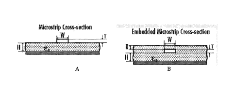
FIGS. lA and 1B show two variants of microstrip which includes embedded
microstrip and
coated microstrip, both of which add some dielectric above the microstrip
conductor.
FIG. 2A shows a side view of the start of the method in which a lap and
polished
photodefinable glass substrate that is used, e.g., a 300gm thick lap and
polished
photodefinable glass.
FIG. 2B shows a side view DC Sputter a uniform coating of titanium between 200
A and
10,000 A thick on the back of the substrate.
FIG. 2C shows a side view of the electroplate a copper ground plane on the
back of the
substrate. The copper ground plane should be between 0.5 gm and 10 gm thick on
the back
of the substrate.
FIG. 2D shows a top view of the device formed using a chrome mask with a
triangular or
trapezoidal clear region to exposed the photodefinable glass substrate. The
substrate is 6" in
diameter. The exposure is with approximately 20J/cm2 of 310nm light. The
length L is 100
CA 03082624 2020-05-13
WO 2019/136024 PCMJS2018/068184
6
[tm to 200 gm; Width W2 is 10 gm; Width W1 is 50 gm. Next, heat the exposed
photodefinable glass to 450 C for 60 min.
FIG. 2E-1 shows atop view of the etch the exposed photodefinable glass in 10%
HF solution
down copper/metal ground plane, and FIG. 2E-2 shows a side view of the same
device
shown in FIG. 2E-1.
FIG. 2F-I shows a top view of the fill the etched region with a low loss
tangent material that
is a different dielectric constant than the APEX Glass, and FIG. 2F-2 shows a
side view of
the same device shown in FIG. 2F-1.
FIG. 2G shows a top view of the device after applying a photoresist and expose
a pattern
develop and removed the exposed pattern for the microwave stripline.
FIG 2H shows a top view after DC Sputter a coating of titanium between 200 A
and 10,000
A thick on the front of the substrate/photoresist.
FIG. 21 is a top view after removing the photoresist using a solvent to expose
a titanium
pattern on the photodefinable glass substrate.
FIG. 2J is a top view after electroplating a copper in the patterned titanium.
The copper
should be between 0.5 gm and 10 gm thick on the back of the substrate.
FIG. 2K is a top view after the impedance matching micro strip line is used to
connect a
variety of devices depicted here as Device 1 and Device 2.
FIG. 3A shows a cross-sectional view of the transmission lines of the present
invention.
.. FIG. 3B is a graph that shows a comparison of the losses of the low loss
micro-transmission
line of the present invention, when compared to standard glass.
DETAILED DESCRIPTION OF THE INVENTION
While the making and using of various embodiments of the present invention are
discussed
in detail below, it should be appreciated that the present invention provides
many applicable
inventive concepts that can be embodied in a wide variety of specific
contexts. The specific
embodiments discussed herein are merely illustrative of specific ways to make
and use the
invention and do not delimit the scope of the invention.
To facilitate the understanding of this invention, a number of terms are
defined below.
Terms defined herein have meanings as commonly understood by a person of
ordinary skill
in the areas relevant to the present invention. Terms such as "a", "an" and
"the" are not
CA 03082624 2020-05-13
WO 2019/136024 PCMJS2018/068184
7
intended to refer to only a singular entity, but include the general class of
which a specific
example may be used for illustration. The terminology herein is used to
describe specific
embodiments of the invention, but their usage does not limit the invention,
except as
outlined in the claims.
The present invention relates to creating an impedance matching between RF
device on the
same substrate. Devices such as Filters, Inductors, Capacitors Resistors, Time
Delay
Networks, Directional Couplers Biased Tees, Fixed Couplers, Phase Array
Antenna, Filters
& Diplexers, Baluns, Power Combiners/Dividers and Power Amplifiers have
different
impedance. These devices are often connected by a conductive structure. The
conductive
structure can be comprised of a microstrip, stripline, coplanar wave guide,
grounded
coplanar wave guide, and coaxial waveguide. We convenience and brevity will
refer to all
of these potential conductive structures as a microstrip line. When an RF
signal is
transmitted between different devices on a microstrip line the impedance
difference can
create losses or reflected signals. Creating an impedance matching structure
reduces losses,
improves signal quality (increasing data rates and transmission distance),
reduces losses and
improves battery life.
Photosensitive glass structures have been suggested for a number of
micromachining and
microfabrication processes such as integrated electronic elements in
conjunction with other
elements systems or subsystems. Semiconductor microfabrication using thin film
additive
processes on semiconductor, insulating or conductive substrates is expensive
with low yield
and a high variability in performance. An example of additive micro-
transmission can be
seen in articles Semiconductor microfabrication processes by Tian et al. rely
on expensive
capital equipment; photolithography and reactive ion etching or ion beam
milling tools that
generally cost in excess of one million dollars each and require an ultra-
clean, high-
production silicon fabrication facility costing millions to billions more.
This invention
provides creates a cost effective glass ceramic electronic individual device
or as an array of
devices with a uniform response across a large broadband low loss transmission
structure.
Microstrip transmission lines consist of a conductive strip of width "W" and
thickness "t"
and a wider ground plane, separated by a dielectric layer (a.k.a. the
"substrate") of thickness
"H" as shown in the figure below. Microstrip is by far the most popular
microwave
transmission line, especially for microwave integrated circuits and MMICs. The
major
advantage of microstrip over stripline is that all active components can be
mounted on top of
the board. The disadvantages are that when high isolation is required such as
in a filter or
CA 03082624 2020-05-13
WO 2019/136024 PCMJS2018/068184
8
switch, some external shielding may have to be considered. Given the chance,
microstrip
circuits can radiate, causing unintended circuit response. A minor issue with
microstrip is
that it is dispersive, meaning that signals of different frequencies travel at
slightly different
speeds. Microstrip does not support a TEM mode, because of its filling factor.
For coupled
lines, the even and odd modes will not have the same phase velocity. This
property is what
causes the asymmetric frequency of microstrip bandpass filters, for example.
Microstrip. FIGS. lA and 1B shows two variants of microstrip include embedded
microstrip
and coated microstrip, both of which add some dielectric above the microstrip
conductor.
Effective dielectric constant. Because part of the fields from the microstrip
conductor exist
in air, the effective dielectric constant "Keff' is somewhat less than the
substrate's dielectric
constant (also known as the relative permittivity). The effective dielectric
constant Ear of
microstrip is calculated by:
w
AM I-4 <4
kslf
"
" _____________________ ' ___ 4- i., esAAi
9 v.km &
(
Olen 1
õt} H
____________________ + ____ 1.
W =
The effective dielectric constant is a seen to be a function of the ratio of
the width to the
microstrip line to the height of substrate (W/H), as well as the dielectric
constant of the
substrate material.
Characteristic impedance. Characteristic impedance Zo of microstrip is also a
function of the
ratio of the height to the width W/H (and ratio of width to height H/W) of the
transmission
line, and also has separate solutions depending on the value of W/H. The
characteristic
impedance Zo of microstrip is calculated by:
CA 03082624 2020-05-13
WO 2019/136024 PCMJS2018/068184
9
= =
k: )
, -= = __ !Id .8-======.4. id#4.491
" =
\ = =
=
wifrso 1
H)
420
õ
= r W ' :W =
M`'= .1c =f. .393 +
H 3 = s.11
-
Impedance matched RF circuit requires optimizing the:
a. Thickness of the substrate H bellow the mircrostrip line;
b. Dielectric constant of the substrate bellow the mircrostrip line; and
c. Width of the mircrostrip line.
The present invention includes a method to fabricate a substrate with RF
impedance
matching device structures RF devices on a photodefinable glass ceramic
substrate. In
general the impedance matching device is formed by etching a triangular via
through the
photodefinable glass ceramic, then filling the with a non conductive media
with a different
dielectric constant that is different from the photodefinable glass ceramic
substrate. The
metal line that connects the RF devices transverses the length of the filled
triangular shaped
region from the narrow to wide end.
To address these needs, the present inventors developed a glass ceramic (APEX
Glass
ceramic) as a novel packaging and substrate material for semiconductors, RF
electronics,
microwave electronics, and optical imaging. APEX Glass ceramic is processed
using first
generation semiconductor equipment in a simple three step process and the
final material
can be fashioned into either glass, ceramic, or contain regions of both glass
and ceramic.
Photo-etchable glasses have several advantages for the fabrication of a wide
variety of
microsystems components.
Microstructures have been produced relatively inexpensively with these glasses
using
conventional semiconductor processing equipment. In
general, glasses have high
temperature stability, good mechanical and electrically properties, and have
better
chemical resistance than plastics and many metals. Photoetchable glass is
comprised of
lithium-aluminum-silicate glass containing traces of silver ions. When exposed
to UV-light
10
within the absorption band of cerium oxide, the cerium oxide acts as
sensitizers,
absorbing a photon and losing an electron that reduces neighboring silver
oxide to
form silver atoms, e.g.,
Ce3+ + Ag+ = Ce' + Ag
The silver atoms coalesce into silver nanoclusters during the baking process
and
induce nucleation sites for crystallization of the surrounding glass. If
exposed to UV
light through a mask, only the exposed regions of the glass will crystallize
during
subsequent heat treatment.
This heat treatment must be performed at a temperature near the glass
transformation temperature (e.g., greater than 465 C. in air). The crystalline
phase is
more soluble in etchants, such as hydrofluoric acid (HF), than the unexposed
vitreous,
amorphous regions. The crystalline regions etched greater than 20 times faster
than the
amorphous regions in 10% HF, enabling microstructures with wall slopes ratios
of
about 20:1 when the exposed regions are removed. See T.R. Dietrich et al.,
"Fabrication technologies for microsystems utilizing photoetchable glass,"
Microelectronic Engineering 30, 497 (1996).
In general photoetchable glass and is composed of silicon oxide (SiO2) of 75-
85% by
weight, lithium oxide (Li2O) of 7-11% by weight, aluminum oxide (A1203) of 3-
6% by
weight, sodium oxide (Na2O) of 1-2% by weight, 0.2-0.5% by weight antimonium
trioxide
(Sb203) or arsenic oxide (As203), silver oxide (Ag2O) of 0.05-0.15% by weight,
and
cerium oxide (Ce02) of 0.01- 0.04% by weight. As used herein the terms "APEX
Glass ceramic", "APEX glass" or simply "APEX" is used to denote one embodiment
of the glass ceramic composition of the present invention.
APEX composition provides three main mechanisms for its enhanced performance:
(1)
The higher amount of silver leads to the formation of smaller ceramic crystals
which
are etched faster at the grain boundaries, (2) the decrease in silica content
(the main
constituent etched by the HF acid) decreases the undesired etching of
unexposed
material, and (3) the higher total weight percent of the alkali metals and
boron oxide
produces a much more homogeneous glass during manufacturing.
The present invention includes a method for fabricating a low loss RF
impedance
matching structure in APEX Glass structure for use in forming angled
structures,
mirrors and glass ceramic materials used in electromagnetic transmission and
filtering
Date recue/date received 2021-10-27
CA 03082624 2020-05-13
WO 2019/136024 PCMJS2018/068184
11
applications. The present invention includes an angled structure created in
the multiple
planes of a glass-ceramic substrate, such process employing the (a) exposure
to excitation
energy such that the exposure occurs at various angles by either altering the
orientation
of the substrate or of the energy source, (b) a bake step and (c) an etch
step. Angle sizes
can be either acute or obtuse. The curved and digital structures are
difficult, if not
infeasible to create in most glass, ceramic or silicon substrates. The present
invention has
created the capability to create such structures in both the vertical as well
as horizontal
plane for glass-ceramic substrates.
Ceramicization of the glass is accomplished by exposing a region of the APEX
Glass
substrate to approximately 20J/cm2 of 310nm light. In one embodiment, the
present
invention provides a quartz/chrome mask containing a variety of concentric
circles with
different diameters.
The present invention includes a method for fabricating a RF impedance
matching
microstrip line used to connect different electronic devices fabricated in or
attached to the
photosensitive glass. The RF impedance matching microstrip line can connect
devices
including but not limited to: Filters, Inductors, Capacitors Resistors, Time
Delay Networks,
Directional Couplers Biased Tees, Fixed Couplers, Phase Array Antenna, Filters
&
Diplexers, Baluns, Power Combiners/Dividers and Power Amplifiers. The
photosensitive
glass substrate can having a wide number of compositional variations including
but not
limited to: 60 - 76 weight % silica; at least 3 weight % K20 with 6 weight % -
16 weight %
of a combination of K20 and Na2O; 0.003-1 weight % of at least one oxide
selected from the
group consisting of Ag2O and Au,O; 0.003-2 weight % Cu2O; 0.75 weight % - 7
weight ()/0
B203, and 6 - 7 weight % A1203; with the combination of B203; and A1203 not
exceeding 13
weight %; 8-15 weight % Li2O; and 0.001 ¨ 0.1 weight % Ce02. This and other
varied
.. compositions are generally referred to as the APEX glass.
The exposed portion may be transformed into a crystalline material by heating
the glass
substrate to a temperature near the glass transformation temperature. When
etching the glass
substrate in an etchant such as hydrofluoric acid, the anisotropic-etch ratio
of the
exposed portion to the unexposed portion is at least 30:1 when the glass is
exposed to a
broad spectrum mid-ultraviolet (about 308-312 nm) flood lamp to provide a
shaped glass
structure that have an aspect ratio of at least 30:1, and to provide a lens
shaped glass
structure. The mask for the exposure can be of a halftone mask that provides a
continuous
grey scale to the exposure to form a curved structure for the micro lens. A
digital mask used
CA 03082624 2020-05-13
WO 2019/136024 PCMJS2018/068184
12
with the flood exposure can be used to produce a diffractive optical element
or Fresnel lens.
The exposed glass is then baked typically in a two-step process. Temperature
range heated
between of 420 C-520 C for between 10 minutes to 2 hours, for the coalescing
of silver
ions into silver nanoparticles and temperature range heated between 520 C-620
C for
between 10 minutes and 2 hours allowing the lithium oxide to form around the
silver
nanoparticles. The glass plate is then etched. The glass substrate is etched
in an etchant, of
HF solution, typically 5% to 10% by volume, wherein the etch ratio of exposed
portion to
that of the unexposed portion is at least 30:1. Create the impedance matching
strip line
structure requires this general processing approach.
FIG. 2A shows a side view of the start of the method in which a lap and
polished
photodefinable glass substrate 10 that is used, e.g., a 300gm thick lap and
polished
photodefinable glass.
FIG. 2B shows a side view DC Sputter a uniform coating of titanium 12 between
200 A and
10,000 A thick on the back of the photodefinable glass substrate 10.
FIG. 2C shows a side view of the electroplate a copper ground plane on the
back of the
substrate. The copper ground plane 14 should be between 0.5 gm and 10 p.m
thick on the
back of the photodefinable glass substrate 10.
FIG. 2D shows a top view of the device formed using a chrome mask 16 with a
triangular or
trapezoidal clear region to exposed the photodefinable glass substrate 10. The
substrate is 6-
in diameter. The exposure is with approximately 20J/cm2 of 310nm light. The
length L is
100 gm to 200 gm; Width W2 is 10 gm; Width W1 is 50 gm. Next, heat the exposed
photodefinable glass to 450 C for 60 min.
FIG. 2E-1 shows a top view of the etch the exposed photodefinable glass
substrate 10 in
10% HF solution down copper/metal ground plane 18, and FIG. 2E-2 shows a side
view of
the same device shown in FIG. 2E-1.
FIG. 2G-1 shows a top view of the fill the etched region with a lovv loss
tangent material that
is a different dielectric constant than the APEX Glass, and FIG. 2G-2 shows a
side view of
the same device shown in FIG. 2G-1. For a low dielectric constant requirement
the
patterned structure can be filled with a spin on glass from Allied Signal
(methyl siloxane
spin-on-glass). For high dielectric requirements the patterned structure can
be filled with,
e.g., a BaTiO3 paste from Advance Materials. Next, the feature is heat treated
on the
photodefinable glass substrate 10 to 600 C for 1 hour.
CA 03082624 2020-05-13
WO 2019/136024 PCMJS2018/068184
13
FIG. 2H shows a top view of the device after applying a photoresist 20 and
expose a pattern
develop and removed the exposed pattern for the microwave stripline.
FIG 21 shows a top view after DC Sputter a coating of titanium 22 between 200
A and
10,000 A thick on the front of the substrate/photoresist 10.
FIG. 2J is a top view after removing the photoresist using a solvent to expose
a titanium
pattern 24 on the photodefinable glass substrate.
FIG. 2K is a top view after electroplating a copper in the patterned titanium.
The copper
should be between 0.5 gm and 10 gm thick on the back of the substrate. If the
application
requires an air gap then the wafer is exposed to a 0.5% HF etch removing the
spin on glass.
FIG. 2L is a top view after the impedance matching micro strip line is used to
connect a
variety of devices depicted here as Device 1 and Device 2 at contacts 26.
FIG. 3A top shows a cross-sectional view of the transmission line of the
present invention
that includes: grounds 30, conductor 32, photodefinable glass substrate 34 and
ground 36.
FIG. 3B (bottom) shows another example of the transmission line of the present
invention
that includes an air-gap, and the figures shows the grounds 30, the conductor
32, the
photodefinable glass substrate 34, the ground 36, and air gaps (dielectric)
38.
FIG. 3B is a graph that shows a comparison of the losses of the low loss micro-
transmission
line of the present invention, when compared to standard glass.
Thus, the present invention has built and simulated a micro strip line using
air as the
dielectric material, the width of the dielectric trapezoid W1 is at 100 um and
is reduced to
W2 to 50 urn. Again, the loss tangent for APEX glass is defined to be .02 at
60 GHz. All
metals are 10 gm thick Cu with a 500A Ti adhesion layer, however, the skilled
artisan will
recognize that the requirements of a device (overall power, current,
resistance, etc.) will
dictate the materials used, the thickness and length of the device, and the
tolerance to signal-
to-noise ratio, etc., to accommodate the specific requirements of the device,
as will be
known to the skilled artisan in light of the specification and the formulas
hereinabove. The
photodefinable glass substrate used in this example has a 6- diameter and 300
gm thickness,
however, both of those can easily be varied as will be known to the skilled
artisan. The
insertion loss for this 1 cm long line is 0.495 dB at 60 GHz. This level of
insertion loss is
unprecedented in RF devices particularly compared to PCB based RF products.
14
The present inventors used a photo-definable glass ceramic (APEX ) Glass
Ceramic or
other photo definable glass as a novel substrate material for semiconductors,
RF
electronics, microwave electronics, electronic components and/or optical
elements. In
general, a photo definable glass is processed using first generation
semiconductor
equipment in a simple three step process and the final material can be
fashioned into either
glass, ceramic, or contain regions of both glass and ceramic. Low loss micro-
transmission
transmission lines are the base line structure that enable, e.g.: Time Delay
Networks,
Directional Couplers Biased Tees, Fixed Couplers, Phase Array Antenna, Filters
and
Diplexers, Baluns, Power Combiners/Dividers and Power Amplifiers, at
frequencies from
MHz to THz devices thereby dramatically improving the efficiency and
performance. The
low loss micro-transmission transmission lines are the base line structure
that enable, e.g.:
Time Delay Networks, Directional Couplers Biased Tees, Fixed Couplers, Phase
Array
Antenna, Filters and Diplexers, Baluns, Power Combiners/Dividers and Power
Amplifiers,
at frequencies from MHz to THz devices while reducing the size. Alternatively,
the low
loss micro-transmission transmission lines at frequencies from MHz to THz
devices can
thereby dramatically improving the efficiency and performance and reducing the
size.
It is contemplated that any embodiment discussed in this specification can be
implemented
with respect to any method, kit, reagent, or composition of the invention, and
vice versa.
Furthermore, compositions of the invention can be used to achieve methods of
the
invention.
It will be understood that particular embodiments described herein are shown
by way of
illustration and not as limitations of the invention. The principal features
of this invention
can be employed in various embodiments without departing from the scope of the
invention. Those skilled in the art will recognize, or be able to ascertain
using no more
than routine experimentation, numerous equivalents to the specific procedures
described
herein. Such equivalents are considered to be within the scope of this
invention and are
covered by the claims.
All publications and patent applications mentioned in the specification are
indicative of
the level of skill of those skilled in the art to which this invention
pertains.
The use of the word "a" or "an" when used in conjunction with the term
"comprising" in
the claims and/or the specification may mean "one," but it is also consistent
with the
Date recue/date received 2021-10-27
15
meaning of "one or more," "at least one," and "one or more than one." The use
of the term
"or" in the claims is used to mean "and/or" unless explicitly indicated to
refer to
alternatives only or the alternatives are mutually exclusive, although the
disclosure
supports a definition that refers to only alternatives and "and/or."
Throughout this
application, the term "about" is used to indicate that a value includes the
inherent variation
of error for the device, the method being employed to determine the value, or
the variation
that exists among the study subjects.
As used in this specification and claim(s), the words "comprising" (and any
form of
comprising, such as "comprise" and "comprises"), "having" (and any form of
having, such
as "have" and "has"), "including" (and any form of including, such as
"includes" and
"include") or "containing" (and any form of containing, such as "contains" and
"contain")
are inclusive or open-ended and do not exclude additional, unrecited elements
or method
steps. In embodiments of any of the compositions and methods provided herein,
"comprising" may be replaced with "consisting essentially of' or "consisting
of'. As used
herein, the phrase "consisting essentially of' requires the specified
integer(s) or steps as
well as those that do not materially affect the character or function of the
claimed
invention. As used herein, the term "consisting" is used to indicate the
presence of the
recited integer (e.g., a feature, an element, a characteristic, a property, a
method/process
step or a limitation) or group of integers (e.g., feature(s), element(s),
characteristic(s),
property(ies), method/process steps or limitation(s)) only.
The term "or combinations thereof" as used herein refers to all permutations
and
combinations of the listed items preceding the term. For example, "A, B, C, or
combinations thereof' is intended to include at least one of: A, B, C, AB, AC,
BC, or
ABC, and if order is important in a particular context, also BA, CA, CB, CBA,
BCA,
.. ACB, BAC, or CAB. Continuing with this example, expressly included are
combinations
that contain repeats of one or more item or term, such as BB, AAA, AB, BBC,
AAABCCCC, CBBAAA, CABABB, and so forth. The skilled artisan will understand
that
typically there is no limit on the number of items or terms in any
combination, unless
otherwise apparent from the context.
As used herein, words of approximation such as, without limitation, "about",
"substantial"
or "substantially" refers to a condition that when so modified is understood
to not
necessarily be absolute or perfect but would be considered close enough to
those of
Date recue/date received 2021-10-27
16
ordinary skill in the art to warrant designating the condition as being
present. The extent to
which the description may vary will depend on how great a change can be
instituted and
still have one of ordinary skill in the art recognize the modified feature as
still having the
required characteristics and capabilities of the unmodified feature. In
general, but subject
to the preceding discussion, a numerical value herein that is modified by a
word of
approximation such as "about" may vary from the stated value by at least 1,
2, 3, 4, 5, 6,
7, 10, 12 or 15%.
All of the compositions and/or methods disclosed and claimed herein can be
made and
executed without undue experimentation in light of the present disclosure.
While the
compositions and methods of this invention have been described in terms of
preferred
embodiments, it will be apparent to those of skill in the art that variations
may be applied
to the compositions and/or methods and in the steps or in the sequence of
steps of the
method described herein without departing from the scope of the invention. All
such
similar substitutes and modifications apparent to those skilled in the art are
deemed to be
within the scope of the invention as defined by the appended claims.
Date recue/date received 2021-10-27