Note: Descriptions are shown in the official language in which they were submitted.
DESCRIPTION
LED LIGHT SOURCE MECHANISM, TELEPHONE SET, AND
METHOD FOR FORMING LED LIGHT SOURCE
Technical Field
[0001]
The present disclosure relates to an LED (Light Emitting Diode)
light source mechanism, a telephone set, and a method for forming an
LED light source. In particular, the present disclosure relates to an
LED light source mechanism, a telephone set, and a method for
forming an LED light source, capable of illuminating a wide range
without causing unevenness in the illumination even when only one
LED is used as a light source.
Background Art
[0002]
Operation buttons (i.e., operation keys) and indicator lamps for
user interfaces as well as a handset are disposed on the surface of the
housing of a telephone set. As an example of a telephone set, a key
telephone like one disclosed in Japanese Unexamined Patent
Application Publication No. 2004-235736 "Key Telephone Set and Key
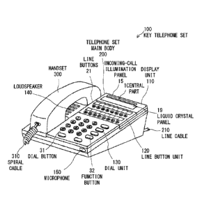
Telephone System" is described. Fig. 6 is a perspective view showing
its external appearance. Fig. 6 is a perspective view showing an
example of an external appearance of a key telephone set in the present
state.
[0003]
As shown in Fig. 6, in a key telephone set 100B, a telephone set
main body 200B is connected to a handset 300 through a spiral cable
310. Further, a main unit that performs the overall control of the key
telephone system (not shown) is connected to the telephone set main
body 200B through a line cable 210.
[0004]
A display unit 110B, a line button unit 120, a dial unit 130, a
Date Recue/Date Received 2020-06-08
2
loudspeaker 140, and a microphone 150 are arranged on the upper
surface and the side surfaces of the telephone set main body 200B.
The display unit 110B includes an incoming-call lamp 14 for visually
displaying an incoming-call state, and a liquid-crystal panel 19 for
displaying a communication state of the key telephone set 100B and
various button operation states. Further, the line button unit 120
includes a plurality of line buttons 21 for selecting an extension line
and an outside line. Further, the dial unit 130 includes a plurality of
dial buttons 31 and a plurality of function buttons 32.
Summary of Invention
[0005]
However, in the present-state art related to the present
disclosure, the incoming-call lamp 14 provided in the display unit
110B is usually disposed at the right shoulder of the telephone set
main body 200B as shown in Fig. 6. As a result, in the above-
described position of the incoming-call lamp 14, its visibility is
insufficient. Therefore, a user may not be able to see the incoming-
call lamp 14 because he/she is distracted therefrom by a button
operation task or what is displayed on the screen of the liquid-crystal
panel 19, or because the incoming-call lamp 14 is hidden behind
documents placed on a desk. Therefore, even if an incoming call
occurs and the incoming-call lamp 14 is lighted, the user may not be
able to recognize the incoming call.
[0006]
Therefore, in order to improve the visibility by a user, it is
desirable that a laterally-long and wide area in the upper area of the
display unit 110B of the telephone set main body 200B be illuminated
in a diffused manner, instead of illuminating only the right shoulder
part as in the case of the incoming-call lamp 14 shown in Fig. 6.
However, regarding the cost, it is desirable that the number of LEDs
(Laser Emitting Diodes) that serve as the light source for the laterally-
long diffused illumination not be increased, i.e., be only one. Further,
it is desirable to provide a light source mechanism that can uniformly
Date Recue/Date Received 2020-06-08
3
illuminate an illumination surface in both the left and right directions
by moving the position of the one LED and thereby disposing it at the
center of the upper area of the display unit 110B, instead of disposing
it in the right shoulder thereof, and diffusing light emitted from the
LED in both the left and right directions (the lateral direction) of the
upper area in a light guide part (a lens part) that guides the light from
the LED to the illumination surface.
[0007]
However, in the present-state art related to the present
disclosure, even if the light emitted from the one LED, which serves as
the light source, is diffused in both the left and right directions of the
upper area of the display unit 110B of the telephone set body 200B in
the state where the LED is disposed at or near the center of the upper
area thereof, the light lays are concentrated at the center where the
LED is located and hence the light cannot be sufficiently diffused to
both the left and right ends, thus causing unevenness in the
illumination on the illumination surface. This situation cannot be
improved even when a material containing a diffusing agent for
diffusing light is used as the material for the light guide part and the
illumination surface.
[0008]
Figs. 7A and 7B are schematic drawings showing an internal
structure of an LED light source mechanism when an LED serving as a
light source is disposed at the central position of the upper area of the
display unit 110B of the key telephone set 100B shown in Fig. 6, and
show a case where an illumination surface is formed in the lateral
direction of the upper area of the display unit 110B of the key
telephone set 100B, i.e., in both the left and right directions of the
upper area from the central position thereof. Note that Fig. 7A is a
perspective view showing a structure of an LED light source
mechanism 50B located in the upper area of the telephone set main
body 200B as viewed obliquely from the front in the perspective view
shown in Fig. 6, in which the inside of the telephone set main body
200B is shown in a perspective manner. Further, Fig. 7B is a
Date Recue/Date Received 2020-06-08
4
perspective view showing an internal structure forming the LED light
source mechanism 50B shown in Fig. 7A as viewed from the top.
[0009]
As shown in the LED light source mechanism 50B shown in Fig.
7B, directly below an illumination surface 11B formed in the upper
area of the display unit 110B of the telephone set main body 200B,
i.e., at the central position in the left/right direction of the
illumination surface 11B (the position directly below the central part
1), an LED 10, which serves as the light source is disposed with a light
guide part (a lens part that leads light to the illumination surface 11B)
interposed therebetween so that the LED 10 is opposed to the
illumination surface 11B. Further, a reflection surface 12B for
reflecting light from the LED 10 and thereby guiding the light in the
direction toward the illumination surface 11B is formed so as to
surround the illumination surface 11B, the LED 10, and the light
guiding part. Further, the illumination surface 11B has a planar shape
that is laterally long in both the right and left directions, and the
reflection surface 12B has a planar shape that is inclined in a stepwise
manner according to the distance from the end of the illumination
surface 11B so that light emitted from the LED 10 is refracted and
reflected in the direction toward the illumination surface 11B. Note
that as shown in Fig. 7B, it is assumed that both ends, i.e., the left end
la and the right end lb of the illumination surface 11B are located on
an extension line that is inclined from the central axis (the central
line) of the LED 10 by an angle of 40 in the left/right direction.
[0010]
Note that in the present-state art, in order to form the
illumination surface 11B and the light guide part in an integrated
manner, while applying two-color molding, a transparent material
containing a diffusing agent for diffusing light is usually used for the
light guide part (the lens part), and a diffusing-agent material made of
a resin containing a diffusing agent, such as PMMA (Poly Methyl
Methacrylate) containing a diffusing agent is used for the illumination
surface 11B (the lighting part). Further, the reflection surface 12B is
Date Recue/Date Received 2020-06-08
5
formed by using a PC (Poly Carbonate) having a light shielding
property and high reflection efficiency on the side surfaces of the
illumination surface 11B and the light guide part (the lens part).
[0011]
A result of quantitative evaluations for light lays in the LED
light source mechanism 50B having the above-described structure will
be described with reference to Fig. 8. Fig. 8 is a schematic drawing
showing a result of ray tracing of the LED light source mechanism 50B
in the present-state art shown in Figs. 7A and 7B, and shows a result
of a ray tracing method based on Snell's law. Note that in Fig. 8, the
light-lay emitting state of the illumination surface 11B and the light
guiding part is left-right symmetrical, so that only the left half of the
light-ray emitting state is schematically shown while omitting the right
half thereof.
[0012]
As shown in the result of the ray tracing shown in Fig. 8, even
when a diffusing agent is used for the illumination surface 11B and the
light guide part, the amount of light rays that are emitted from the
LED 10 and reach the illumination surface 11B in the left end la of the
illumination surface 11B is about half (the number of light rays in the
left half in the result of the evaluation experiment shown in Fig. 8 is
three) of the amount of light rays in the central part 1 thereof which is
located in the place opposed to the LED 10 (the number of light rays in
the left half in the result of the evaluation experiment shown in Fig. 8
is six). That is, while the central part 1 of the illumination surface
11B is strongly illuminated, both ends, i.e., the left and right ends la
and lb thereof are weakly illuminated, thus causing unevenness in the
illumination. Note that as described above, the case where both ends,
i.e., the left and right ends la and lb of the illumination surface 11B
are positioned in the directions of the angles of 40 from the central
axis (the central line) of the LED 10 in the left/right direction as
viewed from the LED 10 is shown.
[0013]
That is, in the present-state LED light source mechanism 50B, as
Date Recue/Date Received 2020-06-08
86665218
6
shown in Figs. 7A and 7B, the reflection surface 12B has the
planar shape and the light incident on the reflection surface 12B is
reflected onto the two-dimensional plane. As a result, there is the
following problem to be solved. That is, although the reflected
light easily reaches the central part 1 of the illumination surface
11B, the light lays that reach both ends, i.e., the left and right
ends la and lb of the illumination surface 11B are reduced.
Further, there is also the following problem to be solved. That is,
since the illumination surface 11B and the light guide part are
formed by using a material containing an expanding agent, the
cost is increased. In addition, when the illumination surface 11B
is illuminated, it is illuminated in a whitish somber color. That
is, it is impossible to illuminate the illumination surface 11B in a
clear and bright illuminated state.
[0014]
(Object of the Present Disclosure)
In view of the above-described problems, an object of the
present disclosure is to provide an LED light source mechanism, a
telephone set, and a method for forming an LED light source,
capable of illuminating a wide range without causing unevenness
in the illumination even when only one LED is used as a light
source.
[0015]
According to an aspect of the present invention, there is
provided an LED light source mechanism configured to use one
LED (Light Emitting Diode) as a light source and illuminate an
illumination surface, the illumination surface being laterally long
and wide in a left/right direction, wherein, a central axis of the
LED is disposed at a position on a center line vertically extending
from a central part in the left-right direction of the illumination
surface in such a manner that the LED faces the illumination
Date recue / Date received 2021 -1 1-22
86665218
6a
surface, the LED light source mechanism has two reflection
surfaces that are formed in a conical shape, the two reflection
surfaces being configured to reflect light that is emitted from the
LED toward an outside of the illumination surface, a center line of
the conical shape is disposed on the central axis of the LED, the
two reflection surfaces are: a first reflection surface having a
conical shape and configured to reflect light from the LED on an
outer-surface side thereof; and a second reflection surface having
a truncated-conical shape, the second reflection surface including
openings for light on both upper and lower surfaces thereof and
configured to reflect light from the LED on an inner-surface side
thereof, and an inner-surface side of the first reflection surface
and the inner-surface side of the second reflection surface are
disposed to be opposed to each other around the central axis of the
LED, wherein the light of the LED enters in a light guide part at
the second reflection surface, the light guide part being
configured to guide light emitted from the LED to the illumination
surface, wherein conical form of the second reflection surface
reduces away from the LED towards the first reflection surface,
which conical form is in-line with the second reflection surface
and increases away from the LED, and the light is reflected on the
second reflection surface at a concave inner side and on the first
reflection surface at a convex outer side.
[0015a]
According to another aspect of the present invention, there
is provided a telephone set comprising a laterally long and wide
horizontal incoming-call illumination panel configured to be
illuminated when a telephone call is received, wherein the
incoming-call illumination panel is formed by the LED light
source mechanism described above.
Date recue / Date received 2021 -1 1-22
86665218
6b
[0015b]
According to another aspect of the present invention, there
is provided a method for forming an LED light source, the LED
light source being configured to use one LED (Light Emitting
Diode) as a light source and illuminate an illumination surface,
the illumination surface being laterally long and wide in a
left/right direction, wherein, a central axis of the LED is disposed
at a position on a center line vertically extending from a central
part in the left-right direction of the illumination surface in such
a manner that the LED faces the illumination surface, the LED
light source mechanism has two reflection surfaces that are formed
in a conical shape, the two reflection surfaces being configured to
reflect light that is emitted from the LED toward an outside of the
illumination surface, a center line of the conical shape is disposed
on the central axis of the LED, the two reflection surfaces are: a
first reflection surface having a conical shape and configured to
reflect light from the LED on an outer-surface side thereof; and a
second reflection surface having a truncated-conical shape, the
second reflection surface including openings for light on both
upper and lower surfaces thereof and configured to reflect light
from the LED on an inner-surface side thereof, and an inner-
surface side of the first reflection surface and the inner-surface
side of the second reflection surface are disposed to be opposed to
each other around the central axis of the LED, wherein the light of
the LED enters in a light guide part at the second reflection
surface, the light guide part being configured to guide light
emitted from the LED to the illumination surface, wherein conical
form of the second reflection surface reduces away from the LED
towards the first reflection surface, which conical form is in-line
with the second reflection surface and increases away from the
LED, and the light is reflected on the second reflection surface at
a concave inner side and on the first reflection surface at a convex
Date recue / Date received 2021 -1 1-22
86665218
6c
outer side.
[0016]
In order to solve the above-described problems, an LED
light source mechanism, a telephone set, and a method for forming
an LED light source according to the present disclosure mainly
adopt characteristic configurations described below.
[0016a]
(1) An LED light source mechanism according to the present
disclosure is
an LED light source mechanism configured to use one LED
(Light Emitting Diode) as a light source and illuminate an
illumination surface, the illumination surface being laterally long
and wide in a left/right direction, in which,
a central axis of the LED is disposed at a position on a
center line vertically extending from a central part in the left-
right direction
Date recue / Date received 2021 -1 1-22
7
of the illumination surface in such a manner that the LED faces the
illumination surface,
the LED light source mechanism has two reflection surfaces that
are formed in a conical shape, the two reflection surfaces being
configured to reflect light that is emitted from the LED toward an
outside of the illumination surface,
a center line of the conical shape is disposed on the central axis
of the LED,
the two reflection surfaces are:
a first reflection surface having a conical shape and configured
to reflect light from the LED on an outer-surface side thereof; and
a second reflection surface having a truncated-conical shape, the
second reflection surface including openings for light on both upper
and lower surfaces thereof and configured to reflect light from the
LED on an inner-surface side thereof, and
an inner-surface side of the first reflection surface and the
inner-surface side of the second reflection surface are disposed to be
opposed to each other around the central axis of the LED.
[0017]
(2) A telephone set according to the present disclosure is
a telephone set including laterally long incoming-call
illumination panel configured to be illuminated when a telephone call
is received, in which
the incoming-call illumination panel is formed by the LED light
source mechanism described in the above-described item (1).
[0018]
(3) A method for forming an LED light source according to the
present disclosure is
a method for forming an LED light source, the LED light source
being configured to use one LED (Light Emitting Diode) as a light
source and illuminate an illumination surface, the illumination surface
being laterally long and wide in a left/right direction, in which,
a central axis of the LED is disposed at a position on a center
line vertically extending from a central part in the left-right direction
Date Recue/Date Received 2020-06-08
8
of the illumination surface in such a manner that the LED faces the
illumination surface,
the LED light source mechanism has two reflection surfaces that
are formed in a conical shape, the two reflection surfaces being
configured to reflect light that is emitted from the LED toward an
outside of the illumination surface,
a center line of the conical shape is disposed on the central axis
of the LED,
the two reflection surfaces are:
a first reflection surface having a conical shape and configured
to reflect light from the LED on an outer-surface side thereof; and
a second reflection surface having a truncated-conical shape, the
second reflection surface including openings for light on both upper
and lower surfaces thereof and configured to reflect light from the
LED on an inner-surface side thereof, and
an inner-surface side of the first reflection surface and the
inner-surface side of the second reflection surface are disposed to be
opposed to each other around the central axis of the LED.
[0019]
According to the LED light source mechanism, the telephone set,
and the method for forming an LED light source in accordance with the
present disclosure, the following effects can be mainly achieved.
[0020]
That is, by forming the reflection surfaces in a conical shape,
even if the laterally long and wide illumination surface is illuminated
by one LED, light emitted from the LED can be diffused in the three-
dimensional directions. Therefore, it is possible to uniformly
illuminate the laterally long and wide illumination surface with a
sufficient amount of light from the central part of the illumination
surface to both the left and right ends thereof without causing
unevenness in the illumination. Therefore, since there is no need to
use a diffusing agent for the illumination surface and the light guide
part, it is also possible to reduce the cost.
Date Recue/Date Received 2020-06-08
9
Brief Description of Drawings
[0021]
Fig. 1 is a perspective view showing an example of an external
appearance of a key telephone set which is an example of a telephone
set according to this example embodiment;
Fig. 2A is a drawing schematically showing an example of an
internal structure of a LED light source mechanism according to this
example embodiment, and is a perspective view showing an external
appearance of an LED light source mechanism 50 located in the upper
area of a telephone set main body 200 as viewed obliquely from the
front in the perspective view shown in Fig. 1, in which the inside of
the telephone set main body 200 is shown in a perspective manner;
Fig. 2B is a perspective view showing an example of an internal
structure of the LED light source mechanism 50 as viewed obliquely
from the rear (from the rear side of the paper) in Fig. 2A in a
perspective manner for explaining a conical shape of a reflection plate;
Fig. 2C is a perspective view of the internal structure of the
LED light source mechanism 50 shown in Fig. 2A as viewed from the
top in a perspective manner for explaining light rays emitted from the
LED;
Fig. 3A is diagram for explaining an example of a method for
achieving an inclination angle of each of a truncated-conical shape and
a conical shape of a first reflection surface and a second reflection
surface shown in Fig. 2B;
Fig. 3B is diagram for explaining the example of the method for
achieving the inclination angle of each of the truncated-conical shape
and the conical shape of the first reflection surface and the second
reflection surface shown in Fig. 2B;
Fig. 4 is a schematic drawing showing an example of a result of
ray tracing of the LED light source mechanism shown in Figs. 2A to
2C;
Fig. 5A is a schematic drawing showing a different example of
the LED light source mechanism shown in Figs. 2A to 2C;
Fig. 5B is a schematic drawing showing the different example of
Date Recue/Date Received 2020-06-08
10
the LED light source mechanism shown in Figs. 2A to 2C;
Fig. 5C is a schematic drawing showing the different example of
the LED light source mechanism shown in Figs. 2A to 2C;
Fig. 6 is a perspective view showing an example of an external
appearance of a key telephone set in present-state art;
Fig. 7A is a schematic drawing showing an internal structure of
an LED light source mechanism in a case where an LED serving as a
light source is disposed at a central position in an upper area of a
display unit of the key telephone set shown in Fig. 6;
Fig. 7B is a schematic drawing showing the internal structure of
the LED light source mechanism in the case where the LED serving as
the light source is disposed at the central position in the upper area of
the display unit of the key telephone set shown in Fig. 6; and
Fig. 8 is a schematic drawing showing a result of ray tracing of
the LED light source mechanism in the present-state art shown in Figs.
7A and 7B.
Description of Embodiments
[0022]
Preferred example embodiments of a LED light source
mechanism, a telephone set, and a method for forming an LED light
source according to the present disclosure will be described hereinafter
with reference to the attached drawings. Further, reference symbols
added in each of the drawings are added for respective components for
the sake of convenience as examples for assisting the understanding
thereof. That is, needless to say, they are not added with the intention
of limiting the present disclosure to the example embodiments shown
in the drawings.
[0023]
(Features of the Present Disclosure)
Prior to explaining an example embodiment according to the
present disclosure, an overview of features of the present disclosure is
described hereinafter. A main feature of the present disclosure is to
make it possible, by using one LED as a LED light source mechanism
Date Recue/Date Received 2020-06-08
11
that illuminates a wide illumination surface having a laterally long
shape (e.g., in the case of a telephone set, an incoming-call
illumination panel having a laterally long shape for informing a user of
an incoming call) and forming reflection surfaces in a conical shape, to
diffuse and guide light emitted from the LED for illuminating the
illumination surface in the three-dimensional directions through a light
guide part. In this way, it is possible to prevent or reduce unevenness
in the illumination on the illumination surface and thereby uniformly
illuminate the illumination surface with sufficient brightness.
[0024]
That is, in the present-state art, as described above, when a wide
illumination surface having a laterally long shape is illuminated by one
LED, although the central part of the illumination surface located on
the central axis of the LED is strongly illuminated, both the left and
right ends of the illumination surface are weakly illuminated, thus
causing unevenness in the illumination. In contrast to this, the main
feature of the present disclosure is to make it possible to strongly
illuminate not only the central part of the illumination surface located
on the central axis of the LED but also both the left and right ends of
the illumination surface even when the illumination surface is a wide
illumination surface having a laterally long shape (i.e., is an
illumination panel) and thereby to uniformly illuminate the entire
illumination surface. Further, in the present disclosure, since there is
no need to use a material containing a diffusing agent for diffusing
light over the illumination surface and the light guide part, the cost
can be reduced.
[0025]
(Example of Configuration of Example Embodiment)
Next, as a specific example of a configuration of a LED light
source mechanism according to this example embodiment, firstly, an
example of a configuration of a key telephone set that illuminates a
wide area having a laterally long shape, instead of illuminating the
incoming-call lamp 14 in the key telephone set described above as the
present-state art with reference to Fig. 6. Fig. 1 is a perspective view
Date Recue/Date Received 2020-06-08
12
showing an example of an external appearance of a key telephone set
which is an example of the telephone set according to this example
embodiment.
[0026]
A key telephone set 100 shown in Fig. 1, which is shown as an
example of the telephone set according to this example embodiment, is
one in which an incoming illumination panel 15 having a laterally long
shape in the left/right direction is disposed in an upper surface area of
a display unit 110 of a telephone set main body 200 instead of
disposing the incoming-call lamp 14 on the right shoulder of the
display unit 110B of the telephone set main body 200B of the key
telephone set 100B shown in Fig. 6. Further, components other than
the incoming illumination panel 15 of the key telephone 100 shown in
Fig. 1 are exactly the same as those of the key telephone 100B shown
in Fig. 6. Therefore, an example of the LED light source mechanism
constituting the incoming-call illumination panel 15 will be described
hereinafter while omitting the descriptions of the components other
than the incoming-call illumination panel 15.
[0027]
As shown in Fig. 1, the incoming-call illumination panel 15 is
formed in a laterally long shape that is wide in the left/right direction
so as to cover substantially the entire upper area of the display unit
110 of the telephone set main body 200. Only one LED that serves as a
light source for lighting, i.e., illuminating the incoming-call
illumination panel 15 is disposed inside the telephone set main body
200. Further, this LED is disposed so that its central axis coincides
with a center line vertically extending from the central part 1 in the
left/right direction of the incoming-call illumination panel 15.
Further, the left and right ends of the incoming-call illumination panel
15 are each positioned in a direction of an angle of 40 from the
central axis of the LED in the left and right sides, respectively.
[0028]
Figs. 2A to 2C are drawings schematically showing an example
of the internal structure of an LED light source mechanism according
Date Recue/Date Received 2020-06-08
13
to this example embodiment. That is, an LED light source mechanism
50 shown in Figs. 2A to 2C is an example of an LED light source
function for constructing an incoming-call illumination panel 15
having a laterally long shape in the upper area of the display unit 110
of the key telephone 100 shown in Fig. 1, and shows an example of a
configuration in which the central axis of an LED that serves as a light
source is disposed directly below the central part in the left/right
lateral direction of the illumination surface forming the incoming-call
illumination panel 15.
[0029]
More specifically, Fig. 2A is a perspective view showing an
external appearance of an LED light source mechanism 50 located in
the upper area of a telephone set main body 200 as viewed obliquely
from the front in the perspective view shown in Fig. 1, in which the
inside of the telephone set main body 200 is shown in a perspective
manner. Further, Fig. 2B is a perspective view showing an example of
an internal structure of the LED light source mechanism 50 as viewed
obliquely from the rear (from the rear side of the paper) in Fig. 2A in
a perspective manner for explaining a conical shape of a reflection
plate. Further, Fig. 2C is a perspective view of the internal structure
of the LED light source mechanism 50 shown in Fig. 2A as viewed
from the top in a perspective manner for explaining light rays emitted
from the LED.
[0030]
As shown in the perspective view showing the external
appearance of the LED light source mechanism 50 shown in Fig. 2A,
the central axis of one LED 10 serving as the light source is disposed
at a position on a center line vertically extending from the position
where the central part in the lateral direction (i.e., the left/right
direction) of the illumination surface 11 forming the incoming
illumination panel 15 is located (i.e., from the center of the
semicircular arc). Further, a reflection surface forming plate 12A is
disposed so as to surround the illumination surface 11, the light guide
part, and the LED 10. Note that as shown in Fig. 2B, reflection
Date Recue/Date Received 2020-06-08
14
surfaces having a conical shape are formed in the reflection surface
forming plate 12A.
[0031]
Further, as shown as a center light ray 2 and a left-end light ray
2a from the LED 10 in Fig. 2C, the central axis of the LED 10 is
disposed at a position on a center line vertically extending from the
central part 1 in the left-right direction of the illumination surface 11
in such a manner that the LED 10 faces the illumination surface 11.
Further, both ends, i.e., the left end la and the right end lb of the
illumination surface 11 are positioned at places in directions of angles
of 40 from the central axis (the center line) of the LED 10 on the left
and right sides on the illumination surface 11.
[0032]
Further, as shown in the perspective view of the internal
structure shown in Fig. 2B, in the LED light source mechanism 50 that
illuminates the illumination surface 11, the reflection surfaces having
the conical shape for reflecting light that is emitted from the LED 10
toward the outside of the incoming-call illumination panel 15, i.e., the
outside of the illumination surface 11 and thereby guiding the light to
the illumination surface 11 are formed in a state where the center line
of the conical shape coincides with the central axis of the LED 10.
Further, as the reflection surfaces having the conical shape, two
reflection surfaces, i.e., a first reflection surface 12a having a conical
shape and a second reflection surface having a truncated-conical shape
are disposed on the reflection surface forming plate 12A, so that light
emitted from the LED 10 is uniformly diffused in the three-
dimensional directions more reliably.
[0033]
The first reflection surface 12a is disposed so that the apex of
the conical shape is oriented from the illumination surface 11 toward
the LED 10, and forms a reflection surface that reflects light emitted
from the LED 10 on the outer-surface side thereof. Meanwhile, the
second reflection surface 12b is disposed in the opposite direction to
that of the first reflection surface 12a so that the second reflection
Date Recue/Date Received 2020-06-08
15
surface 12b is oriented from the LED 10 toward the illumination
surface 11. Further, the second reflection surface 12b includes
openings for light on both the upper and lower surfaces thereof and
forms a reflection surface that reflects light emitted from the LED 10
on the inner-surface side thereof.
[0034]
Note that in order to form the illumination surface 11, the light
guide part (the lens part) and/or the illumination part (the illumination
surface 11) may be formed by using an acrylic resin such as PMMA
(Poly Methyl Methacrylate), which is often used in the present-state
art, or by using any material having excellent illumination efficiency.
However, unlike the present-state art, both the light guide part and the
illumination surface 11 are made of a material(s) containing no
diffusing agent. Further, in order to form the first and second
reflection surfaces 12a and 12b on the side surfaces of the light guide
part (the lens part), they may be formed by using PC (Poly Carbonate)
as in the case of the present-state art, or by using any material as long
as the material has a light shielding property and high reflection
efficiency.
[0035]
Note that in order to facilitate wide diffusion of light emitted
from the LED 10 in the lateral direction (the left/right direction) of
the laterally long illumination surface 11, the first reflection surface
12a is formed by stacking a plurality of layers having truncated-
conical shapes having different inclination angles and one layer having
a conical shape. Meanwhile, the second reflection surface 12b is
formed by stacking a plurality of layers having truncated-conical
shapes and having different inclination angles. Note that regarding the
angle of the inclined surface having the truncated-conical shape or the
conical shape in each of the layers forming the reflection surface of
each of the first and second reflection surfaces 12a and 12b, it is
desirable to select an optimum inclination angle at which the laterally
long illumination surface 11 is uniformly illuminated without causing
unevenness in the illumination state based on results of evaluations
Date Recue/Date Received 2020-06-08
16
carried out by a ray tracing method based on Snell's law.
[0036]
Figs. 3A and 3B are diagrams for explaining an example of a
method for determining an inclination angle of each of the truncated-
conical shape and the conical shape of the first and second reflection
surfaces 12a and 12b shown in Fig. 2B. Fig. 3A is a diagram showing
an arrangement showing a positional relation between the reflection
surface forming plate 12A and the LED 10 shown in Figs. 2A to 2C,
and Fig. 3B is a cross-sectional view showing an example of an
inclination angle between the first and second reflection surfaces 12a
and 12b disposed on the reflection surface forming plate 12A as
viewed in a direction indicted by arrows IIIB-IIIB in Fig. 3A.
[0037]
In the cross-sectional view shown in Fig. 3B, as indicated by a
broken-line arrow, the reflected light, i.e., the light that is emitted
from the LED 10 and reflected by the first reflection surface 12a
having the conical shape is reflected at a small angle with respect to
the lateral direction (the horizontal direction) and is reflected toward
the left and right ends la and lb of the illumination surface 11.
Meanwhile, as indicated by a solid-line arrow, the reflected light
reflected by the second reflection surface 12b having the truncated-
conical shape is reflected at an angle larger than that of the broken-
line arrow with respect to the lateral direction (the horizontal
direction) and is reflected toward the inner sides of the left and right
ends la and lb of the illumination surface 11, i.e., toward places that
are closer to the central part 1 than the left and right ends la and lb
are. Further, in the reflection surface formed of the conical shape and
the truncated-conical shapes having mutually different inclination
angles, since the light is diffused and reflected over a wide range in
the three-dimensional directions (in multiple directions), the reflected
light is repeatedly reflected and eventually reaches various places of
the illumination surface 11.
[0038]
A procedure for determining the inclined surfaces of the first
Date Recue/Date Received 2020-06-08
17
and second reflection surfaces 12a and 12b will be briefly described
hereinafter. Firstly, by applying a ray tracing method based on Snell's
law to the inclination angle between the first and second reflection
surfaces 12a and 12b in the cross section IIIB-IIIB shown in Fig. 3B, a
distribution state of light rays over an angle range from the central
axis of the LED shown in Fig. 3B to 400 in the left and right directions
as viewed from the LED 10, i.e., a distribution state of light rays that
reach the illumination surface 11 is evaluated. Then, the inclination
angle of each of the first and second reflection surfaces 12a and 12b in
the state where a uniform distribution state is obtained as the
distribution state of light rays reaching the illumination surface 11
based on the result of the evaluation may be determined as an optimum
inclination angle. After that, a locus that is obtained by rotating the
central axis of the LED 10 by 360 by using the obtained optimum
inclination angle may be applied as a three-dimensional shape (a
conical shape or a truncated-conical shape) of the first and second
reflection surfaces 12a and 12b. As a result, it is possible to make the
reflected light from the first and second reflection surfaces 12a and
12b reach various places over a wide range on the illumination surface
11, and thereby to uniformly illuminate the laterally long and wide
illumination surface 11 even by the light from the one LED 10.
[0039]
Fig. 4 shows results of evaluations of the amount of light lays in
the LED light source mechanism 50 shown in Figs. 2A to 2C in the
case where the inclination angle between the first and second
reflection surfaces 12a and 12b is set to an optimum angle through the
procedure described above with reference to Figs. 3A and 3B. Fig. 4 is
a schematic drawing showing an example of a result of ray tracing of
the LED light source mechanism 50 shown in Figs. 2A to 2C, and
shows a result of a ray tracing method based on Snell's law. Note that
in Fig. 4, the light-lay emitting state of the illumination surface 11
and the light guiding part is left-right symmetrical, so that only the
left half of the light-lay emitting state is shown while omitting the
right half thereof.
Date Recue/Date Received 2020-06-08
18
[0040]
As shown in the schematic drawing shown in Fig. 4, the amount
of light rays that are emitted from the LED 10 and reach the
illumination surface 11 in both ends, i.e., the left and right ends la
and lb of the illumination surface 11, which is opposed to the LED 10,
is roughly equal (the number of light rays in the left half in the result
of the evaluation experiment shown in Fig. 4 is six) to the amount of
light rays in the central part 1 (the number of light rays in the left half
in the result of the evaluation experiment shown in Fig. 4 is six).
[0041]
That is, even in the LED light source mechanism 50 in which the
wide illumination surface 11 having the laterally long shape is
disposed in the left/right direction and only one LED 10 is disposed at
a position on the center line vertically extending from the central part
1 in the left/right direction of the illumination surface 11, since the
reflected light is diffused in the three-dimensional directions by the
first reflection surface 12a having the conical shape and the second
reflection surface 12b having the truncated-conical shape, the
illumination surface 11 can be uniformly illuminated over its entire
area in a strongly-illuminated state. That is, as described above with
reference to the cross-sectional view shown in Fig. 3B, the reflected
light, i.e., the light that is emitted from the LED 10 and reflected by
the first reflection surface 12a having the conical shape and the second
reflection surface 12b having the truncated-conical shape is diffused
and reflected in the three-dimensional directions (in multiple
directions) on these reflection surfaces and eventually reaches various
places of the illumination surface 11.
[0042]
In this way, even in a state where the illumination surface 11,
including the light guide part, does not contain a diffusing agent, the
light emitted from the LED 10 can be diffused uniformly and widely
over the entire illumination surface 11. Therefore, the central part 1
of the illumination surface 11 having the laterally long shape in the
left/right direction is strongly illuminated, and the entire illumination
Date Recue/Date Received 2020-06-08
19
surface 11 including both ends, i.e., the left and right ends la and lb
is strongly illuminated. As a result, it is possible to uniformly
illuminate the illumination surface 11 without causing unevenness in
the illumination and thereby to improve the visibility by a user.
Further, since there is no need to use a diffusing agent, it is expected
that the cost may be reduced.
[0043]
(Description of Effect of Example Embodiment)
As described above in detail, the following effects are obtained
in this example embodiment.
[0044]
That is, even when one LED 10 is used as the light source as the
LED light source mechanism 50, it is possible, by forming the
reflection surfaces by the first reflection surface 12a having the
conical shape and the second reflection surface 12b having the
truncated-conical shape, to diffuse and reflect light emitted from the
LED 10 in the three-dimensional directions. Therefore, it is possible
to uniformly illuminate the laterally long and wide illumination
surface 11 over a wide range from the central part of the illumination
surface 11 to both the left and right ends thereof with a sufficient
amount of light without causing unevenness in the illumination.
Therefore, there is no need to use a diffusing agent for diffusing light
over the illumination surface 11 and the light guide part, and the
illumination surface 11 is not illuminated with the whitish somber
color. Further, the cost can be reduced.
[0045]
(Other Example Embodiments)
In the above-described example embodiment, as shown in Figs.
2A to 2C, the illumination surface 11 has a flat planar shape.
However, in this example embodiment, slits are formed in the
illumination surface in order to enable the illumination surface to be
clearly and brightly illuminated. Note that in order to make it possible
to form an enormous lens part having a lateral length longer than that
shown in Figs. 2A to 2C (a light guide part that guides light to an
Date Recue/Date Received 2020-06-08
20
illumination surface having a longer shape), a case where the central
part and its nearby area of the illumination surface disposed so as to
be opposed to the LED has a curved shape is shown.
[0046]
That is, Figs. 5A to 5C are schematic drawings showing an
example different from the LED light source mechanism 50 shown in
Figs. 2A to 2C, in which unlike the case shown in Figs. 2A to 2C, the
central part of the illumination surface disposed to be opposed to the
LED has a curved shape and slits are formed between the central part
of the illumination surface and both the left and right ends thereof.
Note that Fig. 5A is a perspective view showing an example of the
external appearance of the LED light source mechanism 50 A different
from that shown in Fig. 2A, and Fig. 5B is a perspective view showing
an example of the internal structure of the LED light source mechanism
50A different from that shown in Fig. 2B as viewed obliquely from the
rear (from the rear side of the paper) in Fig. 5A in a perspective
manner. Further, Fig. 5C is an enlarged perspective view of a part of
an illumination surface 11A shown in Fig. 5B.
[0047]
As shown in the drawing showing the external appearance of the
LED light source mechanism 50A in Fig. 5A and the internal structure
of the LED light source mechanism 50A shown in Fig. 5B, the shape of
the area at and near the central part 1, which is opposed to the LED 10,
of the illumination surface 11A is different from the planer shape
shown in Figs. 2A to 2C. That is, the area at and near the central part
1 has a curved shape in which it is curved in the same direction (from
the front of Fig. 5A to the rear thereof) from both the left and right
sides. Further, on a reflection surface forming plate (not shown)
which is formed in side surface parts on the apex side of the curved
shape, a second reflection surface 12b and a first reflection surface
12a are arranged so that they face the LED 10. Further, on a curved
surface (side surface parts of the curved shape) on the side of the
curved shape opposite to the side thereof on which the second
reflection surface 12b and the first reflection surface 12a are disposed,
Date Recue/Date Received 2020-06-08
21
a third reflection surface 12c is formed in a curved shape as an
additional reflection surface forming part.
[0048]
That is, the area at and near the central part 1 of the
illumination surface 11A is formed in a curved shape in which
reflection surfaces having conical shapes (the second reflection surface
12b and the first reflection surface 12a) are disposed at the position of
the apex of the curved shape in which it is curved in the same direction
from both the left and right sides in such a manner that the reflection
surfaces having the conical shapes face the LED 10. Further, a third
reflection surface 12c having a curved shape is further formed on the
curved surface on the side opposite to the position of the apex where
the reflection surfaces having the conical shapes are disposed.
[0049]
By further forming the third reflection surface 12c as described
above, it is possible to make light emitted from the LED 10 further
reflected in the left/right direction (the lateral direction) by the third
reflection surface 12c and thereby to guide the light over a length
longer than in the case shown in Figs. 2A to 2C in both the left and
right directions (the lateral direction) shown in Figs. 5A to 5C through
the light guide part (the lens). Therefore, even when the illumination
surface 11A has a laterally long shape longer than in the case shown in
Figs. 2A to 2C, it is possible to make light reach both ends, i.e., the
left and right ends la and lb which is located deeper than in the case
shown in Figs. 2A to 2C and thereby to uniformly illuminate the entire
area of the illumination surface 11A. In this way, it is possible, by
forming an enormous lens as the light guiding part, to form a LED
light source mechanism 50A including a wide illumination part 11A
laterally linger than that shown in Figs. 2A to 2C.
[0050]
Further, as shown in the internal structure shown in Fig. 5B and
the enlarged view shown in Fig. 5C, a plurality of slits 13 are formed
between the central part 1 of the illumination surface 11A and the left
and right ends la and lb thereof at appropriate intervals according to
Date Recue/Date Received 2020-06-08
22
the wavelength of light emitted from the LED 10 and at substantially
equal intervals. As a result, it is possible to make, by light that
reaches the slits 13 formed in the illumination surface 11A, light
interfere with each other on the illumination surface 11A, and thereby
to make the illumination surface 11A clearly and brightly illuminated.
Therefore, when the LED 10 emits light, a large area on the
illumination surface 11A is brightly illuminated, thus making it
possible to improve the visibility by a user. Further, in this example
embodiment, similarly to the previously-described example
embodiment, there is no need to use a diffusing agent for the material
for the illumination surface 11A and the light guiding part. Therefore,
when the illumination surface 11A is illuminated, it is not illuminated
with the whitish somber color. That is, it is possible to illuminate the
illumination surface 11A in a brightly and clearly illuminated state.
[0051]
Note that the formation of the slits 13 in the illumination
surface 11A is not limited to the case where a laterally long enormous
illumination surface 11A (an enormous lens) is formed as in the case
shown in Figs. 5A to 5C. That is, needless to say, they may be formed
in the incoming-call illumination panel 15 of the key telephone 100
shown in Fig. 1, or in the illumination surface 11 of the LED light
source mechanism 50 shown in Figs. 2A to 2C. Further, as long as the
visibility by a user can be ensured, an appropriate number of slits 13
may be formed between the central part of the illumination surface and
both the right and left ends thereof, instead of forming the slits 13
over substantially the entire area from the central part 1 of the
illumination surface 11A to the left and right ends la and lb thereof.
[0052]
Configurations of preferable example embodiments according to
the present invention have been explained above. However, it should
be noted that the above-shown example embodiments are merely
examples of the present invention and thus do not limit the present
invention. It will be understood by those of ordinary skill in the art
that various changes in form and details may be made to the example
Date Recue/Date Received 2020-06-08
86665218
23
embodiments without departing from the spirit and scope of the
present invention.
[0053]
That is, although the present invention is explained above
with reference to example embodiments, the present invention is
not limited to the above-described example embodiments. Various
modifications that can be understood by those skilled in the art
can be made to the configuration and details of the present
invention within the scope of the invention.
[0054]
Reference Signs List
[0 05 5]
1 CENTRAL PART
la LEFT END
lb RIGHT END
2 CENTER LIGHT RAY
2a LEFT-END LIGHT RAY
10 LED
11 ILLUMINATION SURFACE
11A ILLUMINATION SURFACE
11B ILLUMINATION SURFACE
12A REFLECTION SURFACE FORMING PLATE
12B REFLECTION SURFACE
12a FIRST REFLECTION SURFACE
12b SECOND REFLECTION SURFACE
12c THIRD REFLECTION SURFACE
13 SLIT
14 INCOMING-CALL LAMP
15 INCOMING-CALL ILLUMINATION PANEL
Date recue / Date received 2021 -1 1-22
24
19 LIQUID CRYSTAL PANEL
21 LINE BUTTONS
31 DIAL BUTTON
32 FUNCTION BUTTON
50 LED LIGHT SOURCE MECHANISM
50A LED LIGHT SOURCE MECHANISM
50B LED LIGHT SOURCE MECHANISM
100 KEY TELEPHONE SET
100B KEY TELEPHONE SET
110 DISPLAY UNIT
110B DISPLAY UNIT
120 LINE BUTTON UNIT
130 DIAL UNIT
140 LOUDSPEAKER
150 MICROPHONE
200 TELEPHONE SET MAIN BODY
200B TELEPHONE SET MAIN BODY
210 LINE CABLE
300 HANDSET
310 SPIRAL CABLE
Date Recue/Date Received 2020-06-08