Note: Descriptions are shown in the official language in which they were submitted.
CA 03085336 2020-06-10
WO 2019/118505
PCT/US2018/065015
IMPROVED ILLUMINABLE CARD
This application claims the priority benefit of U.S. Provisional Patent
Application No.
62/597,762 filed December 12, 2017, entitled "ILLUMINABLE CARDS", which
application is
incorporated herein by reference in its entirety.
BACKGROUND
Single panel cards, and in particular cards sized for ready stowage in and
retrieval from a
wallet or purse, are employed for a wide variety of purposes. For example,
such cards may take
the form of collector cards, access cards, identity cards, loyalty cards,
membership cards, transit
cards and transaction cards (e.g. credit, debit and gift cards). Such cards
are often associated with
a given financial institution and/or merchant of goods and/or services who
issues or otherwise
promotes the distribution/use of such cards. In turn, such cards often
comprise visual and/or
functional features unique to or otherwise associable with a corresponding
merchant and/or
financial institution, thereby enhancing consumer brand recognition and
goodwill in relation to the
merchant and/or financial institution.
In an effort to distinguish one card from another, cards of the described
nature have
incorporated increasingly creative features. However, such features often
entail significant
additional card production expense, thereby curtailing widespread
implementation. For example,
implementation of such features may entail a degree of customization that is
simply too expensive
for limited or even widespread card distributions by smaller or otherwise cost-
conscience financial
institutions and merchants. And, incorporation of such creative features often
accomplishes only
a single one of two competing objectives, i.e. visible card differentiation or
functional card
differentiation.
SUMMARY
The present disclosure encompasses embodiments of improved cards and
production
methodologies that facilitate the implementation of creative visual/functional
illumination features
by providing both card customization and card production efficiencies.
In one embodiment, an illuminable card may include a card body comprising an
electrically
non-conductive carrier layer, and an at least partially light transmissive
(e.g. transparent or
1
CA 03085336 2020-06-10
WO 2019/118505
PCT/US2018/065015
translucent) first core layer overlying and interconnected to the carrier
layer. Further, the
illuminable card may include electrically-conductive first and second contact
pads, supportably
interconnected to the carrier layer in opposing, spaced relation to one
another, for receiving a
power signal from one of an external power supply (i.e. a contactless and/or
contact power supply
not included in the illuminable card) and an on-board power supply (e.g. a
battery or the like), and
an illuminable patch supportably interconnected to the carrier layer for
electrical coupling (e.g.
direct or capacitive coupling) with the first and second contact pads, e.g.
between the first and
second contact pads, for illumination through the first core layer on a first
side of the illuminable
card upon receipt of a power signal at the first and second contact pads.
Such illumination may be provided for aesthetic and/or for functional
purposes. For
example, the illumination may provide a visual indication associated with an
intended functional
use of the illuminable card and/or may provide or otherwise highlight a
desired visual image.
For such purposes, the illuminable card may further include a mask overlying a
portion
of the illuminable patch and defining a predetermined image visible on a first
side of the
illuminable card upon illumination of the illuminable patch. The mask may be
patterned to block
and permit passage of predetermined portions of light emitted by the
illuminable patch to define
the predetermined image.
As may be appreciated, the provision of an illuminable patch and overlying
mask to define
a predetermined image provides numerous advantages relative to design
approaches that rely
strictly upon customized configuration of illumination sources to obtain the
desired image. For
example, in disclosed illuminable card embodiments, a base card design may be
established so that
customization may be readily and inexpensively realized via the utilization of
a mask that provides
the desired visible image upon illumination of the illuminable patch. By way
of example, the
predetermined visible image may correspond with a name, logo, character,
graphics or other visual
representation associated with or otherwise selected by a given entity.
Further, in contemplated embodiments, the first and second contact pads may be
defined
by elongated, first and second contact rails, respectively. In turn, the
utilization of first and second
contact rails facilitates ready positioning of the illuminable patch at a
plurality of different
positions relative thereto during card production, thereby further
facilitating card customization
while advantageously accommodating use of a base card design to yield
production efficiencies.
In that regard, opposing edge portions of said first and second contact rails
may have corresponding
2
CA 03085336 2020-06-10
WO 2019/118505
PCT/US2018/065015
lengths in a first dimension that are each greater than a maximum cross-
dimension of the
illuminable patch in said first dimension. Additionally or alternatively,
opposing edge portions of
the first and second contact rails may have corresponding lengths in a first
dimension that are each
greater than lengths of adjacent, corresponding edge portions of the
illuminable patch in the first
dimension, thereby facilitating positioning of the illuminable patch at a
plurality of different
positions relative thereto.
Further, opposing edge portions of the first and second contact rails may
extend
coincidentally and/or in equispaced relation along the corresponding lengths
thereof. For example,
opposing edge portions of the first and second contact rails may extend in
substantially parallel
relation along the corresponding lengths thereof.
In one approach, a rectangular card body may be provided, wherein the opposing
edge
portions of the first and second contact rails extend in parallel relation to
a peripheral edge of the
card body. For example, the opposing edge portions of the first and second
contact rails may
extend parallel to a length edge or a width edge of the illuminable card,
thereby accommodating
illuminable patch positioning at a plurality of different locations along the
length or the width of
the illuminable card.
In some implementations, the first and second contact rails may each have a
corresponding
substantially constant width along the corresponding lengths thereof In one
approach, the first
and second contact rails may have the same width along the corresponding
lengths thereof.
Further, the first and second contact rails may have substantially equal
corresponding lengths.
In some embodiments, a first part of the edge portion of the first contact
rail may be
overlapped by a corresponding edge portion of the illuminable patch (i.e. in
direct, overlapping
contact therewith), and a second part of the first contact rail may extend
beyond the corresponding
edge portion of the illuminable patch in a first dimension (e.g. extending
beyond either or both
ends of the corresponding edge portion of the illuminable patch). In such
implementations, the
non-overlapped, second part of the edge portion of the first contact rail may
have a corresponding
length in a first dimension that is at least 50%, or even at least 200%, of a
length of the overlapped,
first part of the edge portion of the first contact rail in the first
dimension.
In some embodiments, the mask may comprise a printed mask, e.g. printed on an
inward-
facing side and/or outward facing side of the first core layer. The printed
mask may comprise at
least one or a plurality of printed ink layers, wherein the printed ink is at
least partially opaque or
3
CA 03085336 2020-06-10
WO 2019/118505
PCT/US2018/065015
substantially opaque so as to block passage of predetermined portions of light
emitted by the
illuminable patch to yield the predetermined image.
In one approach, the printed mask may define at least a first portion of a
first print layer
printed on the first core layer. In turn, a second portion of the first print
layer may comprise one
or more of:
printed visible human-readable characters;
printed visible graphics;
a printed visible machine-readable marking; and,
a printed flood layer extending across substantially all of an inward-facing
side or
outward-facing side of the first core layer.
In another approach, the mask may be defined by removing portions a layer that
is at least
partially opaque or substantially opaque so as to permit passage of
predetermined portions of light
emitted by the illuminable patch to yield the predetermined image. For
example, a metal foil layer
with removed portions may be provided between the illuminable patch and the
first core layer.
In some implementations, the first portion and the second portion of the first
print layer may
be printed as part of a continuous printing operation to further facilitate
production efficiencies.
Optionally, a second print layer may be printed on a side of the first core
layer that opposes the
side on which the first print layer is printed, wherein the second print layer
comprises one or more
of:
printed visible human-readable characters;
printed visible graphics;
a printed visible machine-readable marking; and,
a printed flood layer extending across substantially all of an inward-facing
side or
outward-facing side of the first core layer.
In some arrangements, the illuminable patch may comprise an electrically
conductive
matrix (e.g. defined by a plurality of electrically conductive particles) and
a plurality of illuminable
diodes disposed between the first and second contact pads, or rails, wherein
the illuminable diodes
illuminate when a power signal is received at the first and second contact
pads. In one approach,
the diodes may be disposed on the downward-facing side of the carrier layer
with at least a portion
of the electrically conductive matrix disposed over the diodes, wherein a
portion of the electrically
conductive matrix may overlap and thereby directly contact a portion of the
first contact pad, or
4
CA 03085336 2020-06-10
WO 2019/118505
PCT/US2018/065015
rail, and wherein the electrically conductive matrix may be slightly spaced
from or in direct contact
with the second contact pad, or rail. In such arrangements, the carrier layer
may be transparent to
allow light emitted by illuminable patch to pass therethrough.
Optionally, a phosphorescent patch may be provided in overlapping relation to
the
illuminable patch so as to fluoresce upon illumination of the illuminable
patch, e.g. between the
illuminable patch and the mask. The phosphorescent patch may have
substantially the same
configuration as the configuration of the illuminable patch. In one approach,
the phosphorescent
patch may be supportably interconnected to the upward-facing side of the
carrier layer in opposing
relation to the illuminable patch. In another approach, the phosphorescent
patch may be
supportably interconnected to the downward-facing side of the carrier layer,
with the illuminable
patch supportably disposed thereupon (e.g. a plurality of diodes may be
supportably disposed over
the phosphorescent patch with an electrically conductive matrix supportably
disposed over the
diodes).
In some embodiments, the illuminable card may comprise an optional translucent
layer that
is located in overlapping relation to the illuminable patch, between the
illuminable patch and the
overlying mask, and that includes at least a portion that extends to a
peripheral edge of the
illuminable card. In turn, a portion of light emitted by the illuminable patch
may be internally
reflected within the translucent layer and directed to the peripheral edge of
the illuminable card to
illuminate such peripheral edge, thereby providing a distinctive feature to
the illuminable card. In
one approach, the translucent layer may comprise a sheet-like layer that
extends to and about the
entirety of the peripheral edge of the illuminable card. For example, when a
rectangular
illuminable card is provided, each of the length edges and width edges may be
illuminated by the
translucent layer upon illumination of the illuminable patch. Optionally, the
translucent layer may
comprise a fluorescent pigment, or dye.
In contemplated embodiments, the card body may further include a second core
layer
interconnected to the carrier layer on a side opposite to the first core
layer, and/or a metal layer
(e.g. a metal foil layer) interconnected to the carrier layer on a side
opposite to the first core layer.
In conjunction with such embodiments, the first core layer, and the second
core layer and/or metal
layer may be of a common peripheral configuration so that each layer extends
continuously around
a peripheral edge of the illuminable card.
5
CA 03085336 2020-06-10
WO 2019/118505
PCT/US2018/065015
Various approaches may be implemented to provide for the receipt of a power
signal from
an external power supply. In one approach, the illuminable card may comprise a
first antenna,
electrically coupled or couplable at offset locations thereof (e.g. at or near
opposite ends thereof)
to different ones of the first and second contact pads, or rails, for
receiving a contactless signal
from an external source of radio-frequency electromagnetic radiation to
thereby provide a power
signal at the first and second contact pads. In some embodiments, the first
antenna may be
supportably interconnected to the carrier layer. In some implementations, the
first antenna may be
supportably interconnected to the downward-facing side of the carrier layer,
wherein the first
antenna may extend about the first and second contact pads, or rails, and the
illuminable patch. In
other implementations, the first antenna may be supportably interconnected to
the upward-facing
side of the carrier layer, opposite to the downward-facing side of the carrier
layer, wherein the
first antenna may extend in non-overlapping relation to and about the first
and second contact pads,
or rails, and the illuminable patch, and wherein the first antenna is
electrically coupled or couplable
to the first and second contact pads via an electrically conductive bridge
that extends through the
carrier layer.
In some arrangements, a film layer(s) may be interconnected to either or both
sides of the
carrier layer in overlapping relation the components supportably
interconnected to the carrier layer
(e.g. first and second contact pads, illuminable patch, optional first
antenna, optional
phosphorescent patch, optional second antenna referenced below, etc.) to
define a pre-laminated
.. inlay. For example, transparent film layers may be adhesively attached to
and cover the entirety of
each side of the carrier layer and supported components, thereby providing a
pre-laminated inlay
to facilitate assembly and interconnection (e.g. via lamination) with
additional layers of the
illuminable card (e.g. second core layer, metal layer, outer protective
layers, adhesive and/or
thermoset interconnecting layers, etc.).
In some implementations, the illuminable card may include an integrated
circuit (IC) chip
disposed in a pocket that extends into the illuminable card on the first side
thereof, and a second
antenna electrically coupled or couplable to the IC chip for receiving a
contactless signal from an
external contactless chip card reader that includes a source of radio-
frequency electromagnetic
radiation, wherein the contactless signal is received by the first antenna and
the second antenna to
provide a power signal at the first and second contact pads and a combined
power/data signal to
the IC chip, respectively. In the later regard, IC chip and contactless chip
card reader may be
6
CA 03085336 2020-06-10
WO 2019/118505
PCT/US2018/065015
provided for contactless data transmissions therebetween. In contemplated
arrangements, the
second antenna may be supportably interconnected to the carrier member (e.g.
supportably
interconnected to the same side or the opposite side to which the first
antenna and/or first and
second contact pads, or rails, are supportably interconnected).
In some embodiments, the first antenna may comprise a first plurality of
metallic loops
and the second antenna may comprise a second plurality of metallic loops,
wherein the second
plurality of metallic loops extend about the first plurality of metallic
loops, e.g. on the same side
or an opposite side of the carrier layer. Further, the first plurality of
metallic loops and second
plurality of metallic loops may be provided to extend about the first and
second contact pads and
the illuminable patch on the same side or an opposite side of the carrier
layer.
Alternatively, in some embodiments, the illuminable card may include an
integrated circuit
(IC) chip disposed in a pocket that extends into the illuminable card on the
first side thereof,
wherein the first antenna is electrically coupled or couplable to the IC chip
for receiving a
contactless signal from an external contactless chip card reader that includes
a source of radio-
frequency electromagnetic radiation. In turn, the contactless signal is
received by the first antenna
to provide a power signal at the first and second contact pads and a combined
power/data signal to
the IC chip. In the later regard, IC chip and contactless chip card reader may
be provided for
contactless data transmissions therebetween.
In another approach for utilizing an external power supply, the illuminable
card may
comprise an IC chip electrically interconnected to a plurality of contact pads
disposed for receiving
a contact electrical power/data signal from an external contact chip card
reader, wherein the IC
chip and contact chip card reader may be provided for contact data
transmissions therebetween.
In conjunction with such approach, the first and second contact pads, or
rails, may be electrically
interconnected to different ones of the plurality of contact pads and/or
corresponding contact
terminals of the integrated circuit chip for receiving a power signal to
illuminate the illuminable
patch. In one approach, the IC chip and plurality of contact pads may be
disposed in a pocket that
extends in to the illuminable card from the first side thereof. In turn,
metallic, first and second
connection lines may be supportably disposed on the carrier layer and
interconnected to and
between the first and second contact pads, or rails, and different ones of the
plurality of contact
pads and/or corresponding contact terminals of the integrated circuit chip,
respectively.
7
CA 03085336 2020-06-10
WO 2019/118505
PCT/US2018/065015
The first core layer, second core layer, and protective, outer film layers may
comprise a
polymer-based material (e.g. polyvinyl chloride, polyethylene terephthalate,
polyethylene
terephthalate glycol-modified, polyester, and/or polycarbonate). Further, the
carrier layer may
comprise a polymer-based material (e.g. polyethylene terephthalate and/or
polycarbonate).
Additionally, the various layers described herein may be interconnected via
lamination, with
thermo-adhesive polymer-based layers and/or thermosetting, polymer-based
layers disposed
between adjacent one of the layers.
In modified embodiments incorporating one or more of the foregoing features,
an
illuminable card may include a card body comprising interconnected,
electrically non-conductive
first and second carrier layers, and a first core layer overlying and
interconnected to the second
carrier layer. Electrically-conductive first and second contact pads may be
supportably
interconnected to an upward-facing side of the first carrier layer for
receiving a power signal from
one of an external power supply (i.e. a contactless and/or contact power
supply not included in the
illuminable card) and an on-board power supply (e.g. a battery or the like).
Further, an illuminable
patch may be supportably interconnected to a downward-facing side of the
second carrier layer,
facing the first carrier layer, for electrical coupling with the first contact
pad and second contact
pad, wherein the illuminable patch illuminates upon receipt of a power signal
at the first and second
contact pads. Such illumination may be provided through the first core layer
on a first side of the
illuminable card and/or at a peripheral edge of the illuminable card.
In contemplated implementations, the second carrier layer may be transparent
or
translucent. In the later regard, at least a portion of light emitted by the
illuminable patch may be
internally reflected in a translucent second carrier layer and directed to a
peripheral edge of the
illuminable card to illuminate the peripheral edge.
In some embodiments, the illuminable patch may be of an elongate configuration
and
located to extend along at least a portion or an entirety of a peripheral edge
of the illuminable card.
For example, the illuminable patch may extend along and in parallel relation
to one peripheral side
edge, a plurality of peripheral side edges (e.g. opposing and/or contiguous
side edges), or the entire
peripheral edge of a rectangular illuminable card. In one approach, the
illuminable patch may
extend along an entirety of a peripheral edge of the illuminable card to
define a frame-like
configuration (e.g. a rectangular frame). In such embodiments, the illuminable
patch may define
an open field on the second carrier for overlapped positioning relative to one
or more antennas
8
CA 03085336 2020-06-10
WO 2019/118505
PCT/US2018/065015
provided on the first carrier layer, as otherwise described herein. Further, a
phosphorescent patch
may be provided in overlapping relation to the illuminable patch, and may have
a configuration
that is substantially the same as the configuration of the illuminable patch
(e.g. a frame-like
configuration).
In some implementations, the first and second contact pads may be defined by
elongated,
first and second contact rails, respectively. In turn, the illuminable patch
may be configured for
positioning between and electrical coupling with the first and second contact
rails at a plurality of
different positions relative thereto (e.g. the illuminable patch may be a
polygonal, ellipsoid or other
closed configuration and located within a central field of the second carrier
in spaced relation to a
peripheral edge thereof). Such positioning may be defined during card
production, thereby
facilitating card customization while advantageously accommodating use of a
base card design to
yield production efficiencies. Additionally or alternatively, opposing edge
portions of the first and
second contact rails may have corresponding lengths in a first dimension that
are each greater than
a maximum cross-dimension of the illuminable patch in the first dimension.
Further, the opposing
edge portions may have lengths great than adjacent, corresponding edge
portions of the illuminable
patch in the first dimension, thereby facilitating positioning of the
illuminable patch at a plurality
of different positions relative thereto.
Additionally, opposing edge portions of the first and second contact rails may
extend
coincidentally and/or in equispaced relation along the corresponding lengths
thereof. For example,
opposing edge portions of the first and second contact rails may extend in
substantially parallel
relation along the corresponding lengths thereof.
In one approach, a rectangular card body may be provided, wherein the opposing
edge
portions of the first and second contact rails extend in parallel relation to
a peripheral edge of the
card body. For example, the opposing edge portions of the first and second
contact rails may
extend parallel to a length edge or a width edge of the illuminable card,
thereby accommodating
illuminable patch positioning at a plurality of different locations along the
length or the width of
the illuminable card.
In some implementations, the first and second contact rails may each have a
corresponding
substantially constant width along the corresponding lengths thereof In one
approach, the first
and second contact rails may have the same width along the corresponding
lengths thereof.
Further, the first and second contact rails may have substantially equal
corresponding lengths.
9
CA 03085336 2020-06-10
WO 2019/118505
PCT/US2018/065015
In some embodiments, a first part of the edge portion of the first contact
rail may be
overlapped by a corresponding edge portion of the illuminable patch (i.e. in
direct, overlapping
contact therewith), and a second part of the first contact rail may extend
beyond the corresponding
edge portion of the illuminable patch in a first dimension (e.g. extending
beyond either or both
ends of the corresponding edge portion of the illuminable patch). In such
implementations, the
non-overlapped, second part of the edge portion of the first contact rail may
have a corresponding
length in a first dimension that is at least 50%, or even at least 200%, of a
length of the overlapped,
first part of the edge portion of the first contact rail in the first
dimension.
In contemplated embodiments, the illuminable card may comprise a first antenna
for
electrical coupling at offset locations thereof (e.g. at or near opposite ends
thereof) to different
ones of the first and second contact pads, or rails, for receiving a
contactless signal from an external
source of radio-frequency electromagnetic radiation to thereby provide a power
signal at the first
and second contact pads. In some implementations, the first antenna may be
supportably
interconnected to the upward-facing side of the first carrier layer, wherein
the first antenna may
be located to extend about the first and second contact pads, or rails. The
first antenna may be also
located to extend about an illuminable patch that is positioned between the
first and second contact
pads, or rails, for electrical coupling therewith.
Alternatively, or additionally, the first antenna may be located to extend
within and in non-
overlapping relation to an elongated illuminable patch that extends along one
or a plurality of side
edges of a rectangular illuminable card. For example, the first antenna may be
located within an
open field defined by a frame-like illuminable patch, as otherwise described
herein. In such
arrangements, first and second electrical contacts may be supportably disposed
on the downward-
facing side of the second carrier layer in electrical contact with and between
different, offset
portions of the elongated illuminable patch and different ones of the first
and second contact pads,
wherein electrically non-conductive material may be provided between the first
and second
electrical contacts and the first antenna in over-lapped regions thereof
In some embodiments, the illuminable card may include a mask overlying a
portion of an
illuminable patch positioned and defining a predetermined image visible on a
first side of the
illuminable card upon illumination of the illuminable patch. The mask may be
patterned to block
and permit passage of predetermined portions of light emitted by the
illuminable patch to define
the predetermined image.
CA 03085336 2020-06-10
WO 2019/118505
PCT/US2018/065015
In some embodiments, the mask may comprise a printed mask, e.g. printed on an
inward-
facing side and/or outward facing side of the first core layer. The printed
mask may comprise at
least one or a plurality of printed ink layers, wherein the printed ink is at
least partially opaque or
substantially opaque so as to block passage of predetermined portions of light
emitted by the
illuminable patch to yield the predetermined image.
In one approach, the printed mask may define at least a first portion of a
first print layer
printed on the first core layer. In turn, a second portion of the first print
layer may comprise one
or more of:
printed visible human-readable characters;
printed visible graphics;
a printed visible machine-readable marking; and,
a printed flood layer extending across substantially all of an inward-facing
side or
outward-facing side of the first core layer.
In some implementations, the first portion and the second portion of the first
print layer may
.. be printed as part of a continuous printing operation to further facilitate
production efficiencies.
Optionally, a second print layer may be printed on a side of the first core
layer that opposes the
side on which the first print layer is printed, wherein the second print layer
comprises one or more
of:
printed visible human-readable characters;
printed visible graphics;
a printed visible machine-readable marking; and,
a printed flood layer extending across substantially all of an inward-facing
side or outward-
facing side of the first core layer.
In another approach, the mask may be defined by removing portions a layer that
is at least
partially opaque or substantially opaque so as to permit passage of
predetermined portions of light
emitted by the illuminable patch to yield the predetermined image. For
example, a metal foil layer
with removed portions may be provided between the illuminable patch and the
first core layer.
As noted, a phosphorescent patch may be provided in overlapping relation to
the
illuminable patch so as to fluoresce upon illumination of the illuminable
patch, e.g. between the
illuminable patch and the mask. The phosphorescent patch may have
substantially the same
configuration as the configuration of the illuminable patch. In one approach,
the phosphorescent
11
CA 03085336 2020-06-10
WO 2019/118505
PCT/US2018/065015
patch may be supportably interconnected to an upward-facing side of the second
carrier layer in
opposing relation to the illuminable patch. In another approach, the
phosphorescent patch may be
supportably interconnected to the downward facing t side of the second carrier
layer, with the
illuminable patch supportably disposed thereupon.
In contemplated embodiments, the card body may further include a second core
layer
interconnected to the downward-facing side of the first carrier layer, i.e. on
a side opposite to the
second carrier layer, and/or a metal layer (e.g. a metal foil layer)
interconnected to the first carrier
layer on the downward-facing side, i.e. opposite to the second carrier layer.
In conjunction with
such embodiments, the first core layer and the second core layer and/or metal
layer may be of a
common peripheral configuration so that each layer extends continuously around
a peripheral edge
of the illuminable card.
In some arrangements, a film layer(s) may be interconnected to either or both
of the
downward-facing side of the first carrier layer and/or the upward-facing side
of the second carrier
layer in overlapping relation the components supportably interconnected to the
first carrier layer
and second carrier layer (e.g. first and second contact pads, illuminable
patch, optional first
antenna, optional phosphorescent patch, optional second antenna referenced
below, etc.) to define
a pre-laminated inlay. For example, transparent film layers may be adhesively
attached to and
cover the entirety of the downward-facing side of the first carrier layer and
upward-facing side of
the second carrier layer and supported components, thereby providing a pre-
laminated inlay to
facilitate assembly and interconnection (e.g. via lamination) with additional
layers of the
illuminable card (e.g. second core layer, metal layer, outer protective
layers, adhesive and/or
thermoset interconnecting layers, etc.).
The first core layer, second core layer, and protective, outer film layers may
comprise a
polymer-based material (e.g. polyvinyl chloride, polyethylene terephthalate,
polyethylene
terephthalate glycol-modified, polyester, and/or polycarbonate). Further, the
first and second
carrier layers may comprise a polymer-based material (e.g. polyethylene
terephthalate and/or
polycarbonate). Additionally, the various layers described herein may be
interconnected via
lamination, with thermo-adhesive polymer-based layers and/or thermosetting,
polymer-based
layers disposed between adjacent one of the layers.
In some arrangements, the illuminable patch may comprise a substantially
clear,
electrically-conductive layer supportably disposed on a carrier layer for
electrical coupling with a
12
CA 03085336 2020-06-10
WO 2019/118505
PCT/US2018/065015
first contact pad (e.g. direct or capacitive coupling), or rail, provided on
the same or another carrier
layer, an intermediate layer comprising a plurality of illuminable diodes
supportably disposed on
the electrically-conductive layer, and an electrically-conductive pad
supportably disposed on the
intermediate layer for electrical coupling with a second contact pad (e.g.
direct or capacitive
coupling), or rail, provided on the same or another carrier layer. In the
later regard, the electrically-
pad may be electrically isolated from the electrically-conductive layer by a
layer of electrically
non-conductive material disposed therebetween.
The present disclosure further encompasses method embodiments and multiple
card
embodiments in which a plurality of illuminable cards are provided, wherein
each of the cards may
include:
a commonly-configured card body including:
an electrically non-conductive carrier layer; and,
a first core layer overlying and interconnected to the carrier layer,
wherein the first core layer is at least partially light transmissive; and,
commonly-configured, electrically-conductive first and second contact pads, or
rails,
supportably interconnected to said carrier layer in opposing, spaced relation
to one another,
for receiving a power signal from one of an external power supply and an on-
board power
supply.
Further, for a first portion of said plurality of illuminable cards each
corresponding
illuminable card may include:
a commonly-configured first illuminable patch, supportably disposed for
electrical
coupling with the corresponding first and second contact pads, or rails, for
illumination
upon receipt of a power signal at the corresponding first and second contact
pads, or rails;
and,
a commonly-configured first mask overlying at least a portion of the
corresponding first
illuminable patch and defining a first predetermined image visible on a first
side of the
illuminable card upon illumination of the corresponding first illuminable
patch.
Additionally, for a second portion of the plurality of illuminable cards, each
corresponding
illuminable card further may include:
13
CA 03085336 2020-06-10
WO 2019/118505
PCT/US2018/065015
a commonly-configured second illuminable patch, supportably disposed for
electrical
coupling with the corresponding first and second contact rails for
illumination upon receipt
of a power signal at the corresponding first and second contact pads, or
rails; and,
a commonly-configured second mask overlying at least a portion of the
corresponding
second illuminable patch and defining a second predetermined image visible on
a first side
of the illuminable card upon illumination of the corresponding second
illuminable patch,
wherein said commonly-configured first mask and first predetermined image are
different
from said commonly-configured second mask and said second predetermined image,
respectively.
In some embodiments, for each illuminable card of the first portion of the
plurality of
illuminable cards the corresponding commonly-configured first illuminable
patch may be disposed
in a common first location relative to the corresponding first and second
contact pads, or rails.
Further, for each illuminable card of the second portion of the plurality of
illuminable cards the
corresponding commonly-configured second illuminable patch may be disposed in
a common
second location relative to the corresponding first and second contact pads,
or rails, wherein said
first relative location said second relative location are different.
In some implementations, the commonly-configured first illuminable patch and
the
commonly configured second illuminable patch may be different configurations.
In turn, the
commonly-configured first illuminable patch and the commonly configured second
illuminable
patch may be provided to define substantially common electrical loads (e.g. by
comprising
common areas and common materials).
In some embodiments, for each illuminable card of the first portion of the
plurality of
illuminable cards common first printing (e.g. the same graphics and/or human-
readable printing)
may be provided on the corresponding first core layer, and for each
illuminable card of the second
portion of the plurality of illuminable cards common second printing (e.g. the
same graphics and/or
human-readable printing) may be provided on the corresponding first core
layer, wherein said first
common printing and second common printing are different.
In such method and multiple card embodiments, the illuminable cards comprising
the first
portion of the plurality of card may have additional first common card
features as described in
relation to any of the illuminable card embodiments described herein, with the
exception of visible
account indicia and other personalization data, and the illuminable cards
comprising the second
14
CA 03085336 2020-06-10
WO 2019/118505
PCT/US2018/065015
portion of the plurality of cards may have additional second common card
features as described in
relation to any of the illuminable card embodiments described herein, with the
exception of visible
account indicia and other personalization data. As may be appreciated, one or
more of such
additional first common card features and additional second common card
features may be
different.
Numerous additional features and advantages of the present invention will
become
apparent to those skilled in the art upon consideration of the embodiment
descriptions provided
hereinbelow.
BRIEF DESCRIPTION OF THE DRAWINGS
Fig. 1 is an exploded assembly view of one embodiment of an illuminable card.
Fig. 2A is a front perspective view of the illuminable card embodiment of Fig.
1.
Fig. 2B is aback perspective view of the illuminable card embodiment of Fig.
1.
Fig. 3 is a bottom plan view of a carrier layer and supported components of
the illuminable
card embodiment of Fig. 1.
Fig. 4A is a schematic side cross-sectional view of the carrier layer and
supported
components of the illuminable card embodiment of Fig. 1.
Fig. 4B is a schematic side cross-sectional view of a carrier layer and
supported
components of another illuminable card embodiment.
Fig. 5 is a bottom plan view of a carrier layer and supported components of
another
illuminable card embodiment.
Fig. 6 is a bottom plan view of a carrier layer and supported components of
another
illuminable card embodiment.
Fig. 7 is an exploded assembly view of another embodiment of an illuminable
card.
Fig. 8 is an exploded assembly view of another embodiment of an illuminable
card.
Fig. 9 is an exploded assembly view of another embodiment of an illuminable
card.
DETAILED DESCRIPTION
The following description is not intended to limit the invention to the forms
disclosed
herein. Consequently, variations and modifications commensurate with the
following teachings,
CA 03085336 2020-06-10
WO 2019/118505
PCT/US2018/065015
skill and knowledge of the relevant art, are within the scope of the present
invention. The
embodiments described herein are further intended to explain modes known of
practicing the
invention and to enable others skilled in the art to utilize the invention in
such, or other
embodiments and with various modifications required by the particular
application(s) or use(s) of
the present invention.
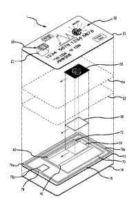
Fig. 1 is an exploded assembly view of one embodiment of an illuminable card 1
that
includes a card body comprising an electrically non-conductive carrier layer
10, and a first core
layer 20 overlying and interconnected to an upward-facing side of the carrier
layer 10. In some
implementations, the first core layer 20 may be at least partially light
transmissive (e.g. transparent
or translucent) or opaque. The illuminable card 1 further includes
electrically-conductive first and
second contact pads 40, 42, defined by corresponding rails in the illustrated
embodiment,
supportably interconnected to the carrier layer 10 in opposing, spaced
relation to one another for
receiving a power signal. Additionally, the illuminable card 1 includes an
illuminable patch 50
supportably interconnected to the carrier layer 10 to provide an electrical
current pathway between
the first and second contact rails 40, 42, wherein the illuminable patch
illuminates upon receipt of
a power signal at the first and second contact rails 40, 42. Such illumination
may be provided
through the first core layer 20 on a first side of the illuminable card 1
and/or through a peripheral
edge of the illuminable card 1. The illumination may be provided for aesthetic
and/or for functional
purposes. For example, the illumination may provide a visual indication
associated with an
intended functional use of the illuminable card and/or may provide or
otherwise highlight a desired
visual image.
As shown, the illuminable card 1 may also include a mask 60 overlying at least
a portion
of the illuminable patch 50 and defining a predetermined image 62 on the first
side of the
illuminable card 1 upon illumination of the illuminable patch 50. As will be
further described, the
mask 60 permits passage of and blocks passage of different portions of the
illumination to provide
the predetermined image 62.
In the embodiment shown in Fig. 1, a first antenna 70 may also be included in
illuminable
card 1 to receive a contactless signal from an external source of radio-
frequency radiation, and to
provide the power signal at the first and second contact rails 40, 42. In that
regard, first antenna 70
may comprise a continuous length of metal defining one or more loops and
having offset locations
(e.g. opposing ends) interconnected to different ones of the first and second
contact rails 40, 42.
16
CA 03085336 2020-06-10
WO 2019/118505
PCT/US2018/065015
As shown, first antenna 70 may also be supportably interconnected to the
carrier layer 10, and may
be disposed to extend about the first and second contact rails 40, 42 and
illuminable patch 50.
In that regard, the first and second contact rails 40, 42, the illuminable
patch 50, and the first
antenna 70 may be disposed on and supportably interconnected to a common side
of carrier layer
10. For example, and as shown in Fig. 1, the first and second contact rails
40, 42, the illuminable
patch 50, and the first antenna 70 may be disposed on and supportably
interconnected to a
downward-facing, first side of carrier layer 10, with metallic cross-
connection bridges between
first antenna 70 and first and second rails 40, 42 being provided on and
through the carrier layer
10.. In other embodiments, the first antenna 70 may be disposed on an upward-
facing, second side
of carrier layer 10, opposite to the first side thereof, with metallic cross-
connection bridges
between first antenna 70 and first and second rails 40, 42 being provided on
and through the carrier
layer 10. By way of example, and as shown in Fig. 1, a metallic bridge 72
(shown in phantom)
may be disposed on and supportably interconnected to carrier layer 10, wherein
metallic cross-
connections may be provided through carrier layer 10 between an end of first
antenna 70 and first
contact rail 40.
In some arrangements, the first and second contact rails 40, 42, first antenna
70, and bridge
72 may be defined by metallic layer(s) supportably disposed on carrier layer
10 (e.g. via plating
and etching operations). In other arrangements, the first and second contact
rails 40, 42, antenna
70, and bridge 72 may be defined by metallic wire supportably disposed on and
partially embedded
in the carrier layer 10.
In some embodiments, the first and second contact rails 40, 42 and the
illuminable patch 50
may be provided to facilitate positioning of the illuminable patch 50 at any
one of a plurality of
different positions relative to the first and second contact rails 40, 42
during manufacture, wherein
the illuminable patch is functional for illumination at any one of the
positions. In that regard,
opposing edge portions of the first and second contact rails 40, 42 may have
corresponding lengths
in a first dimension that are greater than a maximum cross-dimension of the
illuminable patch 50
in the first dimension. Additionally or alternatively, the opposing edge
portions of the first and
second contact rails 40, 42 may have corresponding lengths in a first
dimension that are greater
than the lengths of adjacent, corresponding edge portions of the illuminable
patch 50 in the first
dimension, as shown in Fig. 1.
17
CA 03085336 2020-06-10
WO 2019/118505
PCT/US2018/065015
Further, the opposing edge portions of the first and second contact rails 40,
42 may extend
coincidentally and/or in equispaced spaced relation along the corresponding
lengths thereof. For
example, in the embodiment shown in Fig. 1, the first and second contact rails
40, 42 may extend
in substantially parallel relation to each other and in relation to a
peripheral edge of the illuminable
card 1. Additionally, the first and second contact rails 40, 42 may each have
a corresponding
substantially constant width along the corresponding lengths thereof.
As shown in Fig. 1, a first part of the edge portion of the first contact rail
40 may be
overlapped by the corresponding edge portion of the illuminable patch 50,
wherein a second part
of the first contact rail 40 extends beyond the corresponding edge portion of
the illuminable path
in the first dimension noted above (e.g. the second part may extend in either
or both directions
beyond the overlapped, first part in the first dimension). To facilitate
positioning of the illuminable
patch 50 at a number of different positions relative to first and second
contact rails 40, 42 during
manufacture, the non-overlapped, second part may have a corresponding total
length in the first
dimension that is at least 50%, and in some embodiments at least 200%, of a
length of the
overlapped, first part in the first dimension.
The illuminable patch 50 may assume a range of different configurations,
including a
polygonal configuration (e.g. a rectangular configuration as shown and
described in relation to
Fig. 1,Fig. 7 and Fig. 9 below), or an ellipsoid configuration (e.g. a
circular configuration as shown
and described below in relation to Fig. 6), or an elongate configuration (e.g.
a rectangular frame-
like configuration as shown and described below in relation to Fig. 8).
In at least some contemplated applications in which a plurality of illuminable
cards 1 are
provided that have different corresponding designs, it may be desirable to
employ corresponding
illuminable patches 50 having configurations that each present a substantially
common electrical
load upon receipt of a substantially common power signal. In that regard, in
some implementations
the material(s) utilized to define the illuminable patches 50 may be
substantially the same for each
of the illuminable cards 1, thereby providing for a substantially common load
per unit area upon
illumination. Further, the illuminable patches 50 may be of a substantially
common area. Such
approach is of particular benefit for applications in which the plurality of
illuminable cards 1 with
different corresponding designs are intended for use with external sources of
radio-frequency
electromagnetic radiation that provide contactless power signals at the same
or substantially the
18
CA 03085336 2020-06-10
WO 2019/118505
PCT/US2018/065015
same frequency (e.g. a contactless transaction card reader provided for signal
transmissions
to/from contactless transaction cards at a frequency of about 13.56 Mhz).
As may be appreciated, the mask 60 may define a predetermined pattern that
blocks and
permits passage of predetermined portions of the light emitted by the
illuminable patch 50 to define
the predetermined image 62. For example, mask 60 may be provided to permit a
greater degree of
light passage through a pattern area corresponding with human-readable
characters and other
configurations corresponding with a given logo, name, character, scene or
other image selected by
a given customer.
As shown in Fig. 1, the mask 60 may be disposed in overlying, corresponding
relation to
any of the positions at which the illuminable patch 50 may be located during
manufacture, between
the illuminable patch 50 and the overlying first core layer 20. In one
approach, the mask 60 may
be defined as part of an optional print layer 64 that may be provided on an
inward-facing side of
the first core layer 20. For example, the print layer 64 may comprise an
opaque or substantially
opaque ink layer (e.g. an ink of any desired color) that is printed across at
least a predetermined
portion of an inward-facing side of the first core layer 20 so as to extend
about and thereby define
the predetermined pattern of the mask 60, thereby allowing for light passage
through the
predetermined pattern. In that regard, the print layer 64 may be provided to
comply with visual
opacity requirements of ISO/IEC Standard 7810. In one approach, the print
layer may extend
across the entirety of an inward-facing side or outward-facing side of the
first core layer 20, with
exception of the predetermined pattern of the mask 60. In another approach,
the mask 60 may be
supportably interconnected to the carrier layer 10 in overlying relation to
the illuminable patch 50.
In various embodiments, illuminable card 1 may include one or more additional
features.
For example, an optional phosphorescent patch 80 may be supportably disposed
on the carrier
layer 10 in overlying, corresponding relation to any of the positions at which
the illuminable patch
50 may be located during manufacture, between the underlying illuminable patch
50 and the
overlying mask 60. In such embodiments the phosphorescent patch 80 may have
substantially the
same configuration as the illuminable patch 50.
In one approach, phosphorescent patch 80 may be defined by a coating
comprising a
phosphorescent material that is supportably interconnected to the carrier
layer 10 in overlying
relation to the illuminable patch 50. For example, and as shown in Fig. 1, a
phosphorescent patch
80 may be supportably disposed on the upward-facing, second side of carrier
layer 10, in
19
CA 03085336 2020-06-10
WO 2019/118505
PCT/US2018/065015
overlapping relation to the illuminable patch 50 disposed on the downward-
facing, first side of
carrier layer 10. The phosphorescent patch 80 may be provided to effectively
convert a visible blue
tone illumination of diodes comprising illuminable patch 50 to a visible white
tone illumination,
thereby further enhancing the aesthetic and/or functional features of the
illuminable card 1.
As an additional optional feature, illuminable card 1 may include a
translucent layer 82
that is located in overlying relation to the illuminable patch 50, between the
illuminable patch 50
and the overlying mask 60, and that includes at least a portion to a
peripheral edge of the
illuminable card 1. In turn, a portion of light emitted by the illuminable
patch 50 may be internally
reflected within the translucent layer 82 and thereby directed to the
peripheral edge of the
illuminable card 1 to illuminate the peripheral edge. In one approach, the
translucent layer 82 may
comprise a sheet-like layer that comprises a translucent, polymer-based
material (e.g. a material
comprising an acrylic polymer, a polycarbonate polymer, or the like), and that
extends to a
peripheral edge that extends about the entirety of the peripheral edge of the
illuminable card 1. In
some embodiments, a translucent, polymer-based material may be utilized that
also comprises a
.. fluorescent pigment, or dye, that may be clear or colored for a given
application.
As an additional optional feature, illuminable card 1 may include a film
layer(s) (not
shown), interconnected to either or both sides of the carrier layer 10 in
overlapping relation to the
first and second contact rails 40, 42, illuminable patch 50, first antenna 70,
and/or phosphorescent
patch 80 (if included), so as define a pre-laminated inlay. For example, a
separate film layer may
.. be adhesively attached to and cover the entirety of each side of the
carrier layer 10, thereby yielding
a pre-connected assembly. The film layer(s) may be transparent to allow for
the passage of light
emitted by illuminable patch 50 therethrough. Additionally, printing may be
provided on the film
layer(s). For example, a printed mask 60 may be provided in overlapping
relation to illuminable
patch 50 (e.g. printed as part of a print layer in a manner analogous to print
layer 64 described
herein). The film layer(s) may comprise polymer-based materials.
In contemplated embodiments, the card body of illuminable card 1 may further
include one
or a plurality of additional layers disposed on a downward-facing side of the
carrier layer 10 (e.g.
on an opposing side to the first core layer 20). For example, and as shown in
Fig. 1, an optional
second core layer 30 may be interconnected to a downward-facing side of the
carrier layer 10. As
will be further described below, printing may be provided on either or both of
the first core layer
20 and second core layer 30, wherein such printing is visible from a first
side and/or second side
CA 03085336 2020-06-10
WO 2019/118505
PCT/US2018/065015
of the illuminable card. In turn, a protective, transparent outer film
layer(s) may be provided on an
outward-facing side of each of the first core layer 20 and second core layer
30 (if provided). In
some embodiments, one or both of the outer film layer(s) may be laser
engravable to facilitate the
provision of personalization data, as discussed herein.
The first core layer 20 (e.g. about .006 to .01 inch thick), second core layer
30 (e.g. about .006
to .01 inch thick), and protective, outer film layers may comprise a polymer-
based material (e.g.
polyvinyl chloride, polyethylene terephthalate, polyethylene terephthalate
glycol-modified,
polyester, and/or polycarbonate). Further, the carrier layer 10 (e.g. about
.006 to .012 inch thick)
may comprise a polymer-based material (e.g. polyethylene terephthalate and/or
polycarbonate).
Additionally, the various layers described herein may be interconnected via
lamination, with
thermo-adhesive polymer-based layers or thermosetting, polymer-based layers
disposed between
adjacent one of the layers.
The illuminable card 1 may be provided in a variety of forms. For example, the
illuminable
card 1 may be provided as a collector card, an identity card, an access card,
a loyalty card, a
membership card, a transit card, or a transaction card. In the later regard,
and as shown in Figs. 1,
2A and 2B, illuminable card 1 may be provided with additional features for use
as a transaction
card.
In particular, and as shown in Fig. 2B, the card body of illuminable card 1
may define a card
configuration having at a length L, a width W and a thickness in compliance
with ISO/IEC
Standard 7810. In that regard, the first core layer 20, the second core layer
30 (if provided), and
the outer film layer(s) (if provided) may each be of a common length and
width, in compliance
with ISO/IEC Standard 7810, and thereby accommodating lamination of such
layers in an
interconnected assembly. Additionally, and as shown in Fig. 1, the carrier
layer 10, and optional
translucent layer 82 and pre-laminated inlay film layers, may each be of the
same length and width,
in compliance with ISO/IEC Standard 7810, and thereby accommodating lamination
of such layers
in an interconnected assembly.
Further, in the transaction card form illustrated in Figs. 1, 2A and 2B, the
illuminable card 1
may include a number of features to accommodate use with magnetic stripe card
reader and/or a
contact chip card reader and/or a contactless chip card reader. In particular,
and as shown in Fig.
1, an integrated circuit (IC) chip module 90 (e.g. including at least an IC
chip) and a second antenna
76 may be included for contactless signal transmissions to/from a contactless
chip card reader, e.g.
21
CA 03085336 2020-06-10
WO 2019/118505
PCT/US2018/065015
radio-frequency radiation signals that provide a power/data signal to the IC
chip module 90 via
second antenna 76 and that provide a power signal at first and second contact
rails 40, 42 via first
antenna 70. As may be appreciated, such contactless signals may provide for
data transmissions
between the contactless chip card reader and the IC chip module 90 (e.g. data
transmissions
attendant to the completion of a payment transaction utilizing the illuminable
card 1). In that
regard, the IC chip module 90 and second antenna 76 may be provided for
operation in compliance
with ISO/IEC Standard 14443.
In the embodiment shown in Fig. 1, the second antenna 76 may comprise a
continuous length
of metal supportably interconnected to the carrier layer 10 and defining one
or more outer loop(s)
76a. In one approach, the outer loops(s) 76a may be disposed to extend about
the first antenna 70,
the first and second contact rails 40, 42, and illuminable patch 50 on the
first side of the carrier
layer 10, e.g. the outer loops(s) 76a may extend about a peripheral edge
portion of the carrier layer
10. In other embodiments, the second antenna 76 may be correspondingly
disposed on and
supportably interconnected to the second side of carrier layer 10.
In some arrangements, the second antenna 76 may be defined by metallic
layer(s)
supportably disposed on carrier layer 10 (e.g. via plating and etching
operations). In other
arrangements, the second antenna 70 may be defined by metallic wire
supportably disposed on and
partially embedded in the carrier layer 10.
Various approaches may be utilized to provide for electrical coupling between
the second
antenna 76 and the IC chip module 90. For example, in some approaches the IC
chip module 90
may be embedded within the illuminable card 1 and directly interconnected to
the second antenna
76 (e.g. two opposing ends of the outer loop(s) 76a may be electrically
interconnected to different
ones of a plurality of contacts provided on an IC chip of the IC chip module
90).
In the approach shown in Figs. 1 and 2A the illuminable card 1 may include a
pocket 26 that
extends in to a first side of the illuminable card 1 and that is adapted to
receive the IC chip module
90 for electrical coupling with the second antenna 76. In some
implementations, the IC chip
module 90 may include an electrically non-conductive substrate, an IC chip
supportably
interconnected to an inward-facing side of the substrate, and a plurality of
contact pads supportably
interconnected to an outward-facing side of the substrate and electrically
interconnect through the
substrate to different ones of a plurality of contacts of the IC chip. In the
later regard, the plurality
of contact pads may be provided for contact signal transmissions to/from a
contact chip card reader,
22
CA 03085336 2020-06-10
WO 2019/118505
PCT/US2018/065015
e.g. electrical signals that provide power to the IC chip module 90 and that
provide for data
transmission between the contact chip card reader and the IC chip module 90
(e.g. data
transmissions attendant to the completion of a payment transaction utilizing
the illuminable card
1). In that regard, the IC chip module 90 and plurality of contact pads may be
provided for
operation in compliance with ISO/IEC Standard 7816. As may be appreciated, in
such
implementations the illuminable card 1 may be utilized as a dual interface
transaction card.
In some arrangements, the IC chip module 90 may further include a coupling
antenna
supportably interconnected to an inward-facing side of the substrate and
electrically interconnected
to the IC chip of the IC chip module 90. For example, coupling antenna may
comprise a continuous
length of metal defining one or more loop(s) extending about the IC chip and
electrically
interconnected to different ones of a plurality of contacts of the IC chip. In
turn, the second antenna
76 may be provided for inductive coupling with the coupling antenna of the IC
chip module 90.
More particularly, and as shown in Fig. 1, second antenna 76 may include one
or more inner loop(s)
76b, wherein the outer loop(s) 76a and inner loop(s) 76b are defined by the
continuous length of
metal. The inner loop(s) 76b may be disposed so that, when the IC chip module
90 is secured in
the pocket 26, the inner loop(s) 76b and the coupling antenna of the IC chip
module 90 are
positioned in opposing, spaced relation for inductive coupling. As shown in
Fig. 1, a metallic
bridge 78 (shown in phantom) may be supportably interconnected to an upward-
facing, second
side of carrier layer 10, wherein metallic cross-connections may be provided
through carrier layer
10 to electrically interconnect an end of outer loop(s) 76a and an end of
inner loop(s) 76b.
In another approach, the IC chip module 90 may be provided for direct or
inductive coupling
with the first antenna 70, free from inclusion of a second antenna 76. In such
arrangements, the
first antenna 70 may be utilized to receive contactless RF signals from a
contactless card reader to
provide a power signal at first and second contact rails 40, 42, and to
provide a power/data signal
to the IC chip of IC chip module 90.
In some arrangements, the second antenna 76, first and second contact rails
40, 42, first
antenna 70, and bridge 72 (if necessary) may be defined by metallic layer(s)
supportably disposed
on carrier layer 10 (e.g. via plating and etching operations). In other
arrangements, the second
antenna 76, first and second contact rails 40, 42, antenna 70, and bridge 72
(if necessary) may
defined by metallic wire that is supportably disposed on and partially
embedded in the carrier
layer 10.
23
CA 03085336 2020-06-10
WO 2019/118505
PCT/US2018/065015
Reference is now made to Figs. 2A and 2B which illustrate optional printing 22
visible
from a first side of the illuminable card 1 and optional printing 32 visible
from a second side of
the illuminable card 1, respectively. Printing 22 and/or 32 may comprise one
or more
predetermined print regions that include corresponding graphics (e.g. a
pictorial scene, a logo, a
photo, etc.), corresponding human-readable characters (e.g. numbers, letters,
and/or
representations thereof) and/or one or more corresponding machine-readable
markings (e.g. a bar
code, a multi-dimensional matrix code, etc.), as described in relation to
print layer 64. As shown,
printing 22 may be provided in offset relation to the mask 60. In that regard,
some or all of the
printing 22 may be provided as a portion of the print layer 64, wherein the
print layer 64 may be
defined in a continuous printing operation utilizing a plurality of print
stations.
Printing 22 may be forward printed on an outward-facing side of the
transparent first core
layer 20 (e.g. regardless of whether the first core layer 20 is transparent,
translucent or opaque), or
reverse printed on an inward-facing side of the transparent first core layer
10. Similarly, printing
32 may be forward printed on an outward-facing side of the second core layer
30 (e.g. regardless
of whether the second core layer 30 is transparent, translucent or opaque), or
reverse printed on an
inward-facing side of the second core layer 30 if the second core layer 30 is
transparent.
As shown in Fig. 2A, illuminable card 1 may also include personalization data
24a, 24b
comprising visible indicia indicative of or otherwise corresponding with an
account or record
uniquely associated with the illuminable card 1 (e.g. a payment account
administered by or on
behalf of a card issuer payment institution, a membership account administered
by card issuer
merchant institution, etc.). In some embodiments, visible personalization
indicia 24a and/or 24b
may be provided by embossing the card body of the illuminable card 1 to define
the indicia. In
other embodiments, visible personalization indicia 24a and/or 24b may be
defined by printing on
one or both of the first core layer 20 and/or second core layer 30. In still
other embodiments,
visible personalization indicia 24a and/or 24b may be defined at an outward-
facing surface of the
illuminable card 1 (e.g. by at least one of laser engraving, ink jet printing
and thermoprinting).
The visible personalization indicia 24a may comprise human-readable characters
indicative of a corresponding account (e.g. account number). Further, visible
personalization
indicia 24b may include additional human-readable data corresponding with a
given account,
including a corresponding card expiration date, a corresponding account
service grade level, and/or
corresponding customer-specific data (e.g. customer name, customer duration,
data, etc.). In the
24
CA 03085336 2020-06-10
WO 2019/118505
PCT/US2018/065015
illuminable card 1 embodiment of Figs. 2A and 2B, visible indicia 24a, 24b are
provided for
viewing from a first side of the transaction card 1. In other embodiments,
visible indicia 24a and/or
24b may be also or alternately provided for viewing from the second side of
the transaction card
1. As may be appreciated, the visible indicia 24a, 24b may be provided as
personalization data on
illuminable card 1 as a part of card personalization processing.
As shown in Fig. 2B, illuminable card 1 may also include a magnetic stripe 26
affixed to
the second side of the illuminable card 1. The magnetic stripe 26 may be
encoded during card
personalization with personalization data unique to the illuminable card 1
(e.g. data corresponding
with the account indicated by visible indicia 24a). The magnetic stripe 26 may
be provided in
compliance with ISO/IEC Standard 7811. As further shown, a signature block 27
and/or hologram
28 may also be affixed to the second side of the transaction card 1 (e.g. via
hot-stamping).
Reference is now made to Fig. 3 which illustrates a bottom view of the carrier
layer 10
shown in Fig. 1 (i.e. the first side of the carrier layer 10), together with
the first and second contact
rails 40, 42, the illuminable patch 50, the first antenna 70, and the second
antenna 76, as
supportably interconnected to the downward-facing, first side of the carrier
layer 10. In the
illustrated embodiment, the illuminable patch 50 may include a plurality of
illuminable diodes 54
disposed between the first and second contact rails 40, 42, and an
electrically-conductive matrix
52 disposed over the plurality of diodes 54 between the first and second
contact rails 40, 42,
wherein the plurality of illuminable diodes illuminate when a power signal is
received at the first
and second contact rails 40, 42. In one approach, the plurality of illuminable
diodes 54 may be
provided by disposing a suspension that comprises the diodes on a surface of
the carrier layer 10.
In turn, the electrically-conductive matrix 52 may be provided by disposing
another suspension
that comprises metallic particles (e.g. silver-containing particles) over the
plurality of diodes 54.
As shown, the electrically-conductive matrix 52 may overlap and thereby
directly contact the first
contact rail 40, and may be slightly spaced from the second contact rail 42.
As shown in Fig. 3, illuminable patch 50 may be advantageously located at any
of a
continuum of locations along the first and second contacts 41, 42. Such
locations may extend
across a length of the carrier layer 10, and correspondingly across a
corresponding length of the
illuminable card 1, thereby facilitating customized placement for a given
customer and associated
mask design.
CA 03085336 2020-06-10
WO 2019/118505
PCT/US2018/065015
Fig. 4A illustrates a schematic, side cross-sectional view of the carrier
layer 10 and
supportably interconnected components shown in Fig. 3. As illustrated, the
first and second contact
rails 40, 42, illuminable patch 50, first antenna 70, and second antenna 76
(i.e. as defined by outer
loops 76a and inner loops 76b) may be supportably disposed on the downward-
facing, first side of
carrier layer 10. In turn, bridge 72 and bridge 78 may be supportably disposed
on the second side
of carrier layer 10 and may extend therethrough to establish the illustrated
cross-connections,
otherwise described herein. Fig. 4A further illustrates the optional inclusion
of a phosphorescent
patch 80, supportably interconnected to the upward-facing, second side of
carrier layer 10 in
overlapping relation to illuminable patch 50.Fig. 4B illustrates a schematic,
side cross-sectional
view of a modified embodiment of the carrier layer 10 and supportably
interconnected components
shown in Figs. 3 and 4A. As shown, second antenna 76 and bridge 78 are
supportably disposed on
the upward-facing, second side of carrier layer 10 (e.g. in non-overlapping
relation to first antenna
70).
In view of the unique customization opportunities afforded by the present
invention,
numerous additional embodiments can be recognized. For example, Figs. 5 and 6
illustrate bottom
views of modified embodiments of the carrier layer 10 shown in Fig. 1 (i.e.
the first side of the
carrier layer 10), together with first and second contact rails 40, 42,
illuminable patch 50, first
antenna 70, and second antenna 76, as supportably interconnected to the first
side of the carrier
layer 10. In such modified embodiments, the illuminable patch 50 may include a
plurality of
illuminable diodes 54 disposed between the first and second contact rails 40,
42, and an
electrically-conductive matrix 52 disposed over the plurality of diodes 54
between the first and
second contact rails 40, 42, wherein the plurality of illuminable diodes
illuminate when a power
signal is received at the first and second contact rails 40, 42. In one
approach, the plurality of
illuminable diodes 54 may be provided by disposing a suspension that comprises
the diodes on a
surface of the carrier layer 10. In turn, the electrically-conductive matrix
52 may be provided by
disposing another suspension that comprises metallic particles (e.g. silver-
containing particles)
over the plurality of diodes 54. As shown, the electrically-conductive matrix
52 may overlap and
thereby directly contact the first contact rail 40, and may be slightly spaced
from the second contact
rail 42.
As shown in Fig. 5, illuminable patch 50 may be advantageously located at any
of a
continuum of locations along the first and second contact rails 41, 42. Such
locations may extend
26
CA 03085336 2020-06-10
WO 2019/118505
PCT/US2018/065015
across a width of the carrier layer 10, and correspondingly across a
corresponding width of the
illuminable card 1, thereby facilitating customized placement for a given
customer and associated
mask design.
As shown in Fig. 6, a plurality of sets of first and second contact pads 40a
and 42a, 40b
and 42b, 40c and 42c, may be supportably interconnected to carrier layer 10 to
facilitate
positioning of illuminable patch 50 at any of a corresponding plurality of
locations, thereby
facilitating customized placement for a given customer and associated mask
design. For example,
and as shown in Fig. 6, each set of contact pads may include a stub-like first
contact pad 40a, 40b
and 40c, and a corresponding, complex-shaped second contact pad 42a, 42b and
42c (e.g. an
annular, ring-shaped configuration as shown in Fig. 6), configured to extend
in slightly spaced
relation along at least a portion of a coincidentally-shaped illuminable patch
50. Such an approach
advantageously provides for multi-location positioning of illuminable patch
50, while also
accommodating a complex-shaped illuminable patch 50, as may be desirable for a
given
implementation.
Fig. 7 illustrates another embodiment of an illuminable card 100 that may
include features
in common to the features of illuminable card 1 shown and described above in
relation to Figs. 1-
6, with certain modifications thereto. As such, in relation to the common
features, the same
reference numerals are utilized in Fig. 7 and the feature descriptions
provided above commonly
apply, except as otherwise described or shown in specific relation to Fig. 7.
As shown in Fig. 7, illuminable card 100 includes a card body comprising
interconnected,
electrically non-conductive first and second carrier layers 10, 12 (e.g. each
comprising a polymer-
based material), and first core layer 20 overlying and interconnected to the
second carrier layer 12.
First and second contact pads 40, 42, or rails, and optionally first antenna
70 and/or second antenna
76, may be disposed on and supportably interconnected to a common, upward-
facing side of the
first carrier layer 10. Illuminable patch 50 may be disposed on and
supportably interconnected to
a downward-facing side of the second carrier layer 12, facing the upward-
facing side of the first
carrier layer 10, for electrical coupling with the first and second contact
rails 40, 42 (e.g. via direct
or capacitive coupling), wherein the illuminable patch illuminates upon
receipt of a power signal
at the first and second contact pads 40, 42. Such illumination may be provided
through the first
core layer 20 on a first side of the illuminable card 100 and/or at a
peripheral edge of the
illuminable card 100.
27
CA 03085336 2020-06-10
WO 2019/118505
PCT/US2018/065015
In one approach, a metallic bridge 72 (shown in phantom) may be disposed on
and
supportably interconnected to a downward-facing, first side of the first
carrier layer 10, with
metallic cross-connections at opposing ends through the first carrier layer 10
to the first antenna
70 and first contact rail 40 disposed on an upward-facing, second side of the
first carrier layer 10.
Further, another metallic bridge (shown in phantom) may be disposed on and
supportably
interconnected to a downward-facing, first side of the first carrier layer 10,
metallic cross-
connections at opposing ends through the first carrier layer 10 to offset
locations (e.g. opposing
ends) of the second antenna 76 disposed on an upward-facing, second side of
the first carrier layer
10. In another approach, first antenna 70, and optionally second antenna 76,
may be supportably
disposed on the downward-facing, first side of the first carrier layer 10,
with a metallic bridge
extending through the first carrier layer 10 for cross-connection at opposing
ends to the first
antenna 70 and first contact rail 40, and with another metallic bridge
extending through the first
carrier layer 10 for cross-connection at opposing ends to offset locations
(e.g. opposing ends) of
the second antenna 76 .
As shown in Fig. 7, the first and second contact rails 40, 42 and the
illuminable patch 50
may be provided to facilitate positioning of the illuminable patch 50 at any
one of a plurality of
different positions on second carrier layer 12 relative to the first and
second contact rails 40, 42 on
first carrier layer 10 during manufacture, wherein the illuminable patch is
functional for
illumination at any one of the positions. In that regard, opposing edge
portions of the first and
second contact rails 40, 42 may have corresponding lengths in a first
dimension that are greater
than a maximum cross-dimension of illuminable patch 50 in the first dimension
to accommodate
such variable positioning, and in some embodiments greater than the lengths of
adjacent,
corresponding edge portions of the illuminable patch 50 in the first
dimension, as shown in Fig. 7.
In other embodiments, illuminable card 100 may be modified to provide a
plurality of sets of first
and second contact pads that are disposed on and supportably interconnected to
second carrier
layer 12, e.g. as shown and described in relation to Fig. 6, to facilitate
positioning of illuminable
patch 50 at any of a corresponding plurality of locations, thereby
facilitating customized placement
for a given customer.
The second carrier layer 12 may be one of transparent and translucent. When
second carrier
layer 12 is translucent, at least a portion of light emitted by the
illuminable patch 50 may be
internally reflected within the second carrier layer 12 and directed to a
peripheral edge of the
28
CA 03085336 2020-06-10
WO 2019/118505
PCT/US2018/065015
illuminable card 100 for illumination thereof Optionally, the second carrier
layer 12 may comprise
a fluorescent pigment, or dye. When second carrier layer 12 is transparent or
translucent, at least
a portion of light emitted by the illuminable patch 50 may pass through the
second side of the
second carrier layer 12 for illumination of at least a portion of a first side
of the illuminable card
100. In the later regard, mask 60 may be provided to overlay at least a
portion of the illuminable
patch 50 to define a predetermined image 62 on the first side of the
illuminable card 100 upon
illumination of the illuminable patch 50. The mask 60 may be defined as part
of an optional print
layer 64 that may be provided on an inward-facing side of the first core layer
20. For example, the
print layer 64 may comprise an opaque or substantially opaque ink layer (e.g.
an ink of any desired
.. color) that is printed across at least a predetermined portion of an inward-
facing side of the first
core layer 20 so as to extend about and thereby define the predetermined
pattern of the mask 60,
thereby allowing for light passage through the predetermined pattern. In that
regard, the print layer
64 may be provided to comply with visual opacity requirements of ISO/IEC
Standard 7810. In one
approach, the print layer may extend across the entirety of an inward-facing
side or outward-facing
side of the first core layer 20, with exception of the predetermined pattern
of the mask 60. In
another approach, the mask 60 may be supportably interconnected to the carrier
layer 10 in
overlying relation to the illuminable patch 50.
Phosphorescent patch 80 may be disposed on and supportably interconnected to
the second
carrier layer 12 in overlying relation to at least a portion of illuminable
patch 50, e.g. between at
least portions of illuminable patch 50 and mask 60. The phosphorescent patch
80 may have
substantially the same configuration as the illuminable patch 50.
Phosphorescent patch 80 may be
disposed on and supportably interconnected to the upward-facing side of second
carrier layer 12,
as shown in Fig. 7. Alternatively, phosphorescent patch 80 may be disposed on
and supportably
interconnected to the downward-facing side of second carrier layer 12, between
the downward-
facing side of second carrier layer 12 and at least a portion of illuminable
patch 50 (e.g. at least a
portion of illuminable patch 50 may be disposed on and supportably
interconnected to a
downward-facing side of the phosphorescent patch 80).
As an additional optional feature, illuminable card 100 may include a film
layer(s) (not
shown), interconnected to the downward-facing side of first carrier layer 10
and/or the upward-
facing side of second carrier layer 12 in overlapping relation to the first
and second contact rails
40, 42, illuminable patch 50, first antenna 70, second antenna 80 and/or
phosphorescent patch 80
29
CA 03085336 2020-06-10
WO 2019/118505
PCT/US2018/065015
(if included), so as define a pre-laminated inlay. For example, a separate
film layer may be
adhesively attached to and cover the entirety of the downward-facing side of
first carrier layer 10
and upward-facing side of second carrier layer 12, thereby yielding a pre-
connected assembly. The
film layer(s) may be transparent to allow for the passage of light emitted by
illuminable patch 50
therethrough. Additionally, printing may be provided on the film layer(s). For
example, a printed
mask 60 may be provided in overlapping relation to illuminable patch 50 (e.g.
printed as part of a
print layer in a manner analogous to print layer 64 described herein). The
film layer(s) may
comprise polymer-based materials.
In contemplated embodiments, the card body of illuminable card 100 may further
include
one or a plurality of additional layers disposed on a downward-facing side of
the carrier layer 10
(e.g. on an opposing side to the first core layer 20). For example, and as
shown in Fig. 1, an optional
second core layer 30 may be interconnected to a downward-facing side of the
carrier layer 10. As
described above in relation to illuminable card 1, printing 22, 32 may be
provided on either or both
sides of the first core layer 20 and second core layer 30, respectively,
wherein such printing is
visible from a first side and/or second side of the illuminable card 100. In
turn, a protective,
transparent outer film layer(s) may be provided on an outward-facing side of
each of the first core
layer 20 and second core layer 30 (if provided).
The first core layer 20 (e.g. about .006 to .001 inch thick), second core
layer 30 (e.g. about
.006 to .001 inch thick), and protective, outer film layers may comprise
polymer-based materials
(e.g. polyvinyl chloride, polyethylene terephthalate, polyethylene
terephthalate glycol-modified,
polyester, and/or polycarbonate). Further, the first carrier layer 10 and
second carrier layer 12 (e.g.
about .006 to .012 inch combined thickness) may comprise a polymer-based
material (e.g.
polyethylene terephthalate and/or polycarbonate). Additionally, the various
layers described
herein may be interconnected via lamination, with thermo-adhesive polymer-
based layers or
thermosetting, polymer-based layers disposed between adjacent one of the
layers.
The illuminable card 100 may be provided in a variety of forms. For example,
the
illuminable card 100 may be provided as a collector card, an identity card, an
access card, a loyalty
card, a membership card, a transit card, or a transaction card. In the later
regard, illuminable card
100 may be provided with additional features for use as a transaction card, as
described in relation
to illuminable card 1 shown in Figs. 1, 2A and 2B.
CA 03085336 2020-06-10
WO 2019/118505
PCT/US2018/065015
Fig. 8 illustrates the illuminable card 100 of Fig. 7, with modified
configurations of
illuminable patch 50 on second carrier layer 12 and phosphorescent patch 80.
The illuminable
card 100 shown in Fig. 8 may include features in common to the features of
illuminable card 1 and
illuminable card 100, shown and described above in relation to Figs. 1-6 and
Fig. 7, respectively,
with certain modifications thereto. As such, in relation to the common
features, the same reference
numerals are utilized in Fig. 8 and the feature descriptions provided above
commonly apply, except
as otherwise described or shown in specific relation to Fig. 8.
As shown in Fig. 8, illuminable patch 50 may be of an elongate configuration
that extends
along (e.g. in parallel relation to) at least a portion or an entirety of a
peripheral edge of illuminable
card 100, wherein the illuminable patch 50 is disposed for electrical coupling
with first and second
contact pads 40, 42, for illumination upon the provision of a power signal to
first and second
contact pads 40, 42. In turn, the second carrier layer 12 may be translucent
to yield enhanced edge
illumination about at least one side edge, a plurality of side edges, or an
entire peripheral edge of
illuminable card 100. More particularly, and as shown, illuminable patch 50
may be of a frame-
like, rectangular configuration that defines an open field therewithin on the
second carrier layer
12. In other embodiments, illuminable patch 50 may extend along a single edge,
two opposing,
electrically interconnected edges in a width dimension or length dimension, or
three, electrically
interconnected, contiguous edges of illuminable card 100,
As further illustrated in Fig. 8, the first antenna 70 may be located on first
carrier layer 10
so as to extend within and in non-overlapping relation to the frame-like,
illuminable patch 50 (e.g.
within the open field defined by the frame-like, illuminable patch 50). In
turn, first and second
electrical contacts 52a, 52b may be disposed and supportably interconnected to
the downward-
facing, first side of the second carrier layer 12, in electrical contact with
and between different,
offset portions of the illuminable patch 50 and different ones of the first
and second contact pads
40, 42. In such arrangements, an electrically non-conductive material 54 may
be provided between
the first and second electrical contacts 52, 52b and the first antenna 70 in
over-lapped regions
thereof.
An optional phosphorescent patch 80 may be supportably disposed on the carrier
layer 10
in overlying, corresponding relation to any of the positions at which the
illuminable patch 50 may
be located during manufacture, between the underlying illuminable patch 50 and
the overlying
mask 60. In such embodiments the phosphorescent patch 80 may have
substantially the same
31
CA 03085336 2020-06-10
WO 2019/118505
PCT/US2018/065015
configuration as the illuminable patch 50. For example, and as shown in Fig.
8, phosphorescent
patch may be of a frame-like configuration that coincides with the fame-like
configuration of
illuminable patch 50.
In one approach, phosphorescent patch 80 may be defined by a coating
comprising a
phosphorescent material that is supportably interconnected to the carrier
layer 10 in overlying
relation to the illuminable patch 50. For example, and as shown in Fig. 1, a
phosphorescent patch
80 may be supportably disposed on the upward-facing, second side of carrier
layer 10, in
overlapping relation to the illuminable patch 50 disposed on the downward-
facing, first side of
carrier layer 10. The phosphorescent patch 80 may be provided to effectively
convert a visible blue
tone illumination of diodes comprising illuminable patch 50 to a visible white
tone illumination,
thereby further enhancing the aesthetic and/or functional features of the
illuminable card 1.
Optionally, in addition to frame-like, illuminable patch 50, another
illuminable patch 50a
may be provided on the second carrier layer 12 and located between first and
second contact rails
40, 42, and another phosphorescent patch 80a may be provided in overlapping
relation to
illuminable patch 50a, in a manner analogous to that described above in
relation to the illuminable
patch 50 shown in Fig. 7. In such arrangements, the combined electrical load
presented by
illuminable patch 50 and illuminable patch 50a may be established to be
substantially equal with
the illuminable patches 50 other ones of the embodiments, for the
design/operational purposes
otherwise described herein.
Fig. 9 illustrates another embodiment of an illuminable card 100 that may
include features
in common to the features of illuminable card 1 shown and described above in
relation to Figs. 1-
6, with certain modifications thereto. As such, in relation to the common
features, the same
reference numerals are utilized in Fig. 9 and the feature descriptions
provided above commonly
apply, except as otherwise described or shown in specific relation to Fig. 9.
As shown in Fig. 9, illuminable card 100 includes a card body comprising an
electrically
non-conductive carrier layer 10 and first core layer 20 overlying and
interconnected to the carrier
layer 10, with first and second contact pads 40, 42, or rails, disposed on and
supportably
interconnected to a common side (e.g. downward-facing) of the first carrier
layer 10. Further,
illuminable patch 50 may be disposed on and supportably interconnected to the
same side (e.g.
downward-facing) of the carrier layer 10 for electrical coupling with the
first and second contact
rails 40, 42 (e.g. via direct or capacitive coupling), wherein the illuminable
patch illuminates upon
32
CA 03085336 2020-06-10
WO 2019/118505
PCT/US2018/065015
receipt of a power signal at the first and second contact pads 40, 42. In the
later regard, a single
antenna 76 may be disposed on and supportably interconnected to the carrier
layer 10 and
electrically interconnected at offset locations thereof of to the first and
second contact pads 40, 42
to provide the power signal thereto, and electrically interconnected to IC
chip module 90 to provide
power/data signals.
As shown in Fig. 9, integrated circuit (IC) chip module 90 (e.g. including at
least an IC
chip) and the antenna 76 may be included for contactless signal transmissions
to/from a contactless
chip card reader, e.g. radio-frequency radiation signals that provide a
power/data signal to the IC
chip module 90 via antenna 76 and that provide a power signal at first and
second contact rails 40,
42 via antenna 76. As may be appreciated, such contactless signals may provide
for data
transmissions between the contactless chip card reader and the IC chip module
90 (e.g. data
transmissions attendant to the completion of a payment transaction utilizing
the illuminable card
1). In that regard, the IC chip module 90 and antenna 76 may be provided for
operation in
compliance with ISO/IEC Standard 14443.
In the embodiment shown in Fig. 9, the antenna 76 may comprise a continuous
length of metal
supportably interconnected to the carrier layer 10 and defining one or more
outer loop(s) 76a. In
one approach, the outer loops(s) 76a may be disposed to extend about the first
and second contact
rails 40, 42, and illuminable patch 50 on a common side of the carrier layer
10.
In some arrangements, the antenna 76 may be defined by metallic layer(s)
supportably
disposed on carrier layer 10 (e.g. via plating and etching operations). In
other arrangements, the
antenna 76 may be defined by metallic wire supportably disposed on and
partially embedded in
the carrier layer 10.
Various approaches may be utilized to provide for electrical coupling between
antenna 76 and
the IC chip module 90. For example, in some approaches the IC chip module 90
may be embedded
within the illuminable card 100 and directly interconnected to the antenna 76
(e.g. two opposing
ends of the outer loop(s) 76a may be electrically interconnected to different
ones of a plurality of
contacts provided on an IC chip of the IC chip module 90).
In the approach shown in Fig. 9 the illuminable card 100 may include a pocket
26 that extends
in to a first side of the illuminable card 100 and that is adapted to receive
the IC chip module 90
for electrical coupling with the antenna 76. In some implementations, the IC
chip module 90 may
include an electrically non-conductive substrate, an IC chip supportably
interconnected to an
33
CA 03085336 2020-06-10
WO 2019/118505
PCT/US2018/065015
inward-facing side of the substrate, and a plurality of contact pads
supportably interconnected to
an outward-facing side of the substrate and electrically interconnect through
the substrate to
different ones of a plurality of contacts of the IC chip. In the later regard,
the plurality of contact
pads may be provided for contact signal transmissions to/from a contact chip
card reader, e.g.
electrical signals that provide power to the IC chip module 90 and that
provide for data
transmission between the contact chip card reader and the IC chip module 90
(e.g. data
transmissions attendant to the completion of a payment transaction utilizing
the illuminable card
1). In that regard, the IC chip module 90 and plurality of contact pads may be
provided for
operation in compliance with ISO/IEC Standard 7816. As may be appreciated, in
such
implementations the illuminable card 100 may be utilized as a dual interface
transaction card.
In some arrangements, the IC chip module 90 may further include a coupling
antenna
supportably interconnected to an inward-facing side of the substrate and
electrically interconnected
to the IC chip of the IC chip module 90. For example, coupling antenna may
comprise a continuous
length of metal defining one or more loop(s) extending about the IC chip and
electrically
interconnected to different ones of a plurality of contacts of the IC chip. In
turn, the antenna 76
may be provided for inductive coupling with the coupling antenna of the IC
chip module 90.
More particularly, and as shown in Fig. 9, antenna 76 may include one or more
inner loop(s) 76b,
wherein the outer loop(s) 76a and inner loop(s) 76b are defined by the
continuous length of metal.
The inner loop(s) 76b may be disposed so that, when the IC chip module 90 is
secured in the pocket
26, the inner loop(s) 76b and the coupling antenna of the IC chip module 90
are positioned in
opposing, spaced relation for inductive coupling. As shown in Fig. 9, a
metallic bridge 78 (shown
in phantom) may be supportably interconnected to a second side of carrier
layer 10, wherein
metallic cross-connections may be provided through carrier layer 10 to
electrically interconnect
an end of outer loop(s) 76a and an end of inner loop(s) 76b.
In the embodiments described above, illuminable patch 50 may comprise a
substantially
clear, electrically-conductive layer supportably disposed on carrier layer 10,
or another carrier
layer 12 if provided, for electrical coupling with a first contact pad 40
(e.g. direct or capacitive
coupling), or rail, provided on a carrier layer 10, an intermediate layer
comprising a plurality of
illuminable diodes supportably disposed on the electrically-conductive layer,
and an electrically-
conductive pad supportably disposed on the intermediate layer for electrical
coupling with a
second contact pad 42 (e.g. direct or capacitive coupling), or rail, provided
on the carrier layer 10.
34
CA 03085336 2020-06-10
WO 2019/118505
PCT/US2018/065015
In the later regard, the electrically-conductive pad may be electrically
isolated from the
electrically-conductive layer by a layer of electrically non-conductive
material disposed
therebetween.
Various embodiments may comprise any number of combinations of apparatus
and/or
method features described above and/or hereinbelow. Such combinations may
include those
encompassed by the following Embodiments:
1. An illuminable card, comprising:
a card body, including:
an electrically non-conductive carrier layer; and,
a first core layer overlying and interconnected to a first side of the carrier
layer,
wherein the first core layer is at least partially light transmissive;
electrically-conductive first and second contact pads, supportably
interconnected to the
carrier layer in opposing, spaced relation to one another, for receiving a
power signal from one of
an external power supply and an on-board power supply;
an illuminable patch, supportably interconnected to the carrier layer between
the first and
second contact rails to illuminate upon receipt of a power signal at the first
and second contact
rails; and,
a mask overlying at least a portion of the illuminable patch and defining a
predetermined
.. image visible on a first side of the illuminable card upon illumination of
the illuminable patch.
2. An illuminable card as recited in Embodiment 1, wherein the first and
second
contact pads are defined by first and second contact rails, respectively, and
wherein opposing edge
portions of said first and second contact rails have corresponding lengths in
a first dimension that
.. are each greater than a maximum cross-dimension of the illuminable patch in
said first dimension.
3. An illuminable card as recited in Embodiment 1 or Embodiment 2, wherein
said
opposing edge portions of said first and second contact rails extend
coincidentally along said
corresponding lengths thereof.
35
CA 03085336 2020-06-10
WO 2019/118505
PCT/US2018/065015
4.
An illuminable card as recited in any one of Embodiments 1-3, wherein said
opposing edge portions of the first and second contact rails extend in
substantially parallel relation
along the corresponding lengths thereof
5. An
illuminable card as recited in any one of Embodiments 1-4, wherein said card
body is rectangular, and wherein the opposing edge portions of the first and
second contact rails
extend in parallel relation to a peripheral edge of the card body.
6. An illuminable card as recited in any one of Embodiments 1-5, wherein
the first
and second contact rails each have a corresponding substantially constant
width along the
corresponding lengths thereof.
7. An illuminable card as recited in any one of Embodiments 1-6, wherein a
first part
of said edge portion of said first contact rail is overlapped by a
corresponding edge portion of the
illuminable patch and a second part of said first contact rail extends beyond
the corresponding
edge portion of the illuminable patch in said first dimension.
8. An illuminable card as recited in any one of Embodiments 1-7, wherein
said second
part has a corresponding length in said first dimension that is at least 50%
of a length of the first
part in said first dimension.
9. An illuminable card as recited in any one of Embodiments 1-8, wherein
the
illuminable patch defines one configuration of the following configurations:
a polygonal configuration; and,
an ellipsoid configuration.
10. An illuminable card as recited in any one of Embodiments 1-9, wherein
the mask
comprises a printed mask printed on one of:
a surface supportably interconnected to the carrier layer; and,
a surface of the first core layer.
36
CA 03085336 2020-06-10
WO 2019/118505
PCT/US2018/065015
11. An illuminable card as recited in any one of Embodiments 1-10, wherein
said
printed mask comprises:
a substantially opaque ink.
12. An illuminable card as recited in any one of Embodiments 1-11, wherein
said mask
comprises:
a printed mask printed on one of an inward-facing surface and an outward-
facing surface
of the first core layer, and defines at least a first portion of a printed
layer.
13. An illuminable card as recited in any one of Embodiments 1-12, wherein
a second
.. portion of the printed layer further comprises at least one of:
visible human-readable characters;
visible graphics;
a visible machine-readable marking; and,
a flood layer extending across substantially all of said one of an inward-
facing
surface and an outward-facing surface of the first core layer.
14. An illuminable card as recited in any one of Embodiments 1-13, further
comprising:
a translucent layer disposed in overlapping relation to the illuminable patch,
between the
illuminable patch and the first core layer, wherein at least one peripheral
edge of the card body is
illuminated by the translucent layer upon illumination of the illuminable
patch.
15. An illuminable card as recited in any one of Embodiments 1-14, wherein
said card
body further comprises at least one or both of:
a second core layer interconnected to said carrier layer on a downward-facing
side thereof;
and,
a second core layer interconnected to said carrier layer on a downward-facing
side thereof
with a metal foil layer interconnected therebetween.
16. An illuminable card as recited in any one of Embodiments 1-15, further
comprising
at least one of:
37
CA 03085336 2020-06-10
WO 2019/118505
PCT/US2018/065015
an antenna, electrically interconnected at offset positions thereof to
different ones of said
first and second contact pads, for receiving a contactless power signal from
an external source of
radio-frequency electromagnetic radiation; and,
an integrated circuit chip electrically interconnected to a plurality of
contact pads disposed
for receiving a contact power signal from an external contact chip card
reader, wherein said first
and second contact pads are electrically interconnected to different contact
terminals of the
integrated circuit chip for receiving said contact power signal.
17. An illuminable card as recited in any one of Embodiments 1-16, further
comprising:
an integrated circuit chip disposed in a pocket located on said first side of
the illuminable
card; and,
an antenna, electrically interconnected at offset positions thereof to
different ones of said
first and second contact pads and directly coupled to or inductably couplable
to the integrated
circuit chip, for receiving a contactless power signal from an external source
of radio-frequency
electromagnetic radiation.
18. An illuminable card as recited in any one of Embodiments 1-17, further
comprising:
a first antenna, supportably interconnected to said carrier layer and
electrically
interconnected at offset positions thereof to different ones of said first and
second contact pads,
for receiving a contactless power signal from an external source of radio-
frequency
electromagnetic radiation.
19. An illuminable card as recited in any one of Embodiments 1-18, further
comprising:
an integrated circuit chip disposed in a pocket located on said first side of
the illuminable
card; and,
a second antenna supportably interconnected to the carrier layer and directly
coupled to or
inductably couplable to the integrated circuit chip, for receiving a
contactless power signal from
an external contactless chip card reader that includes said external source of
radio-frequency
electromagnetic radiation.
38
CA 03085336 2020-06-10
WO 2019/118505
PCT/US2018/065015
20. An illuminable card as recited in any one of Embodiments 1-19, wherein
said first
antenna comprises a first plurality of metallic loops and said second antenna
comprises a second
plurality of antenna loops, wherein said second plurality of metallic loops
extend about said first
plurality of metallic loops on said carrier layer.
21. An illuminable card as recited in any one of Embodiments 1-20, wherein
said
second plurality of metallic loops extend about said first and second contact
pads and said
illuminable patch on said carrier layer.
22. An illuminable card as recited in any one of Embodiments 1-21, further
comprising:
a phosphorescent patch overlying at least a portion of the illuminable patch,
between said
overlying patch and said mask.
23. An illuminable card as recited in any one of Embodiments 1-22, wherein
said
phosphorescent patch is supportably interconnected in direct contact to one of
an upward-facing
side and a downward-facing side of the carrier layer.
24. An illuminable card as recited in any one of Embodiments 1-23, wherein
said
illuminable patch and said first and second contact pads are supportably
interconnected to a
downward-facing side of the carrier layer and said carrier layer is at least
partially light
transmissive, and further comprising:
an antenna, supportably interconnected to the downward-facing side of the
carrier layer
and electrically interconnected at offset positions thereof to different ones
of said first and second
contact pads, for receiving a contactless power signal from an external source
of radio-frequency
electromagnetic radiation.
25. An illuminable card as recited in any one of Embodiments 1-24, wherein
said first
and second contact pads are supportably interconnected to an upward-facing
side of the carrier
layer, and further comprising:
39
CA 03085336 2020-06-10
WO 2019/118505
PCT/US2018/065015
an electrically non-conductive second carrier layer disposed between said
carrier layer and
the overlying first core layer, wherein the illuminable patch is supportably
interconnected to a
downward-facing side of the second carrier layer; and,
an antenna, supportably interconnected to the downward-facing side of the
carrier layer
and electrically interconnected at offset positions thereof to different ones
of said first and second
contact pads, for receiving a contactless power signal from an external source
of radio-frequency
electromagnetic radiation.
26. A plurality of illuminable cards, each comprising:
a commonly-configured card body including:
an electrically non-conductive carrier layer; and,
a first core layer overlying and interconnected to the carrier layer,
wherein the first core layer is at least partially light transmissive; and,
commonly-configured, electrically-conductive first and second contact pads,
supportably
.. interconnected to said carrier layer in opposing, spaced relation to one
another, for receiving a
power signal from one of an external power supply and an on-board power
supply;
wherein for a first portion of said plurality of illuminable cards each
corresponding illuminable
card includes:
a commonly-configured first illuminable patch, supportably disposed for
electrical
coupling with the corresponding first and second contact pads for illumination
upon receipt
of a power signal at the corresponding first and second contact pads; and,
a commonly-configured first mask overlying at least a portion of the
corresponding
first illuminable patch and defining a first predetermined image visible on a
first side of
the illuminable card upon illumination of the corresponding commonly-
configured first
illuminable patch;
wherein for a second portion of the plurality of illuminable cards, each
corresponding illuminable
card further comprises:
a commonly-configured second illuminable patch, supportably disposed for
electrical coupling with the corresponding first and second contact pads for
illumination
upon receipt of a power signal at the corresponding first and second contact
pads; and,
CA 03085336 2020-06-10
WO 2019/118505
PCT/US2018/065015
a commonly configured second mask overlying at least a portion of the
corresponding second illuminable patch and defining a second predetermined
image visible
on a first side of the illuminable card upon illumination of the corresponding
commonly-
configured second illuminable patch, wherein said commonly-configured first
mask and
first predetermined image are different from said commonly-configured second
mask and
said second predetermined image, respectively.
27. A plurality of illuminable cards as recited in Embodiment 26, wherein
for each
illuminable card of the first portion of the plurality of illuminable cards
the corresponding
commonly-configured first illuminable patch is disposed in a common first
location relative to the
corresponding first and second contact pads, wherein for each illuminable card
of the second
portion of the plurality of illuminable cards the corresponding commonly-
configured second
illuminable patch is disposed in a common second location relative to the
corresponding first and
second contact pads, and wherein said first relative location said second
relative location are
different.
28. A plurality of illuminable cards as recited in Embodiment 26 or
Embodiment 27,
wherein for each of the plurality of illuminable cards the corresponding first
and second contact
pads are defined by first and second contact rails, respectively, and wherein
opposing edge portions
of said corresponding first and second contact rails have corresponding
lengths in a first dimension
that are each greater than a maximum cross-dimension of the corresponding
commonly-configured
first illuminable patch in said first dimension or corresponding commonly-
configured second
illuminable patch in said first dimension.
29. A plurality of illuminable cards as recited in any one of Embodiments
26-28,
wherein said commonly-configured first illuminable patch and said commonly
configured second
illuminable patch are different, and wherein said commonly-configured first
illuminable patch and
said commonly configured second illuminable patch define substantially common
electrical loads.
30. A plurality of illuminable cards as recited in any one of Embodiments
26-29,
wherein each of said plurality of cards comprise the features an illuminable
card according to any
of Embodiments 1-25 or 31-84.
41
CA 03085336 2020-06-10
WO 2019/118505
PCT/US2018/065015
31. An illuminable card, comprising:
a card body, including:
an electrically non-conductive carrier layer; and,
a first core layer overlying and interconnected to the carrier layer;
electrically-conductive first and second contact rails supportably
interconnected to said
carrier layer in opposing, spaced relation to one another, for receiving a
power signal from one of
an external power supply and an on-board power supply;
an illuminable patch supportably disposed for electrical coupling with the
first and second
contact rails to illuminate upon receipt of a power signal at the first and
second contact rails,
wherein opposing edge portions of said first and second contact rails have
corresponding lengths
in a first dimension that are each greater than a maximum cross-dimension of
the illuminable patch
in said first dimension.
32. An illuminable card as recited in Embodiment 31, wherein said opposing
edge
portions of said first and second contact rails extend coincidentally along
said corresponding
lengths thereof.
33. An illuminable card as recited in Embodiment 31 or Embodiment 32,
wherein said
opposing edge portions of the first and second contact rails extend in
substantially parallel relation
along the corresponding lengths thereof
34. An illuminable card as recited in any one of Embodiments 31-33, wherein
said card
body is rectangular, and wherein the opposing edge portions of the first and
second contact rails
extend in parallel relation to a peripheral edge of the card body.
35. An illuminable card as recited in any one of Embodiments 31-34, wherein
the first
and second contact rails each have a corresponding substantially constant
width along the
corresponding lengths thereof.
42
CA 03085336 2020-06-10
WO 2019/118505
PCT/US2018/065015
36. An illuminable card as recited in any one of Embodiments 31-35, wherein
a first
part of said edge portion of said first contact rail is overlapped by a
corresponding edge portion of
the illuminable patch and a second part of said first contact rail extends
beyond the corresponding
edge portion of the illuminable patch in said first dimension.
37. An illuminable card as recited in any one of Embodiments 31-36, wherein
said
second part has a corresponding length in said first dimension that is at
least 50 % of a length of
the first part in said first dimension.
38. An illuminable card as recited in any one of Embodiments 31-37, wherein
the
illuminable patch defines one configuration of the following configurations:
a polygonal configuration; and,
an ellipsoid configuration.
39. An illuminable card as recited in any one of Embodiments 31-38, further
comprising:
a mask overlying at least a portion of the illuminable patch and defining a
predetermined
image visible on a first side of the illuminable card upon illumination of the
illuminable patch.
40. An illuminable card as recited in any one of Embodiments 31-39, wherein
the mask
comprises a printed mask printed on one of:
a surface supportably interconnected to the carrier layer; and,
a surface of the first core layer.
41. An illuminable card as recited in any one of Embodiments 31-40 wherein
said
printed mask comprises:
a substantially opaque ink.
42. An illuminable card as recited in any one of Embodiments 31-41, wherein
said
mask comprises:
43
CA 03085336 2020-06-10
WO 2019/118505
PCT/US2018/065015
a printed mask printed on one of an inward-facing surface and an outward-
facing surface
of the first core layer, and defines at least a first portion of a printed
layer.
43. An illuminable card as recited in any one of Embodiments 31-42, wherein
a
second portion of the printed layer further comprises at least one of:
visible human-readable characters;
visible graphics;
a visible machine-readable marking; and,
a flood layer extending across substantially all of said one of an inward-
facing
surface and an outward-facing surface of the first core layer.
44. An illuminable card as recited in any one of Embodiments 31-43, further
comprising:
a translucent layer disposed in overlapping relation to the illuminable patch,
between the
illuminable patch and the first core layer, wherein at least one peripheral
edge of the card body is
illuminated by the translucent layer upon illumination of the illuminable
patch.
45. An illuminable card as recited in any one of Embodiments 31-44, wherein
said
card body further comprises at least one or both of:
a second core layer interconnected to said carrier layer on a downward-facing
side thereof;
and,
a second core layer interconnected to said carrier layer on a downward-facing
side thereof
with a metal foil layer interconnected therebetween.
46. An illuminable card as recited in any one of Embodiments 31-45, further
comprising at least one of:
an antenna, electrically interconnected at offset positions thereof to
different ones of said
first and second contact pads, for receiving a contactless power signal from
an external source of
radio-frequency electromagnetic radiation; and,
an integrated circuit chip electrically interconnected to a plurality of
contact pads disposed
for receiving a contact power signal from an external contact chip card
reader, wherein said first
44
CA 03085336 2020-06-10
WO 2019/118505
PCT/US2018/065015
and second contact pads are electrically interconnected to different contact
terminals of the
integrated circuit chip for receiving said contact power signal.
47. An illuminable card as recited in any one of Embodiments 31-46, further
comprising:
an integrated circuit chip disposed in a pocket located on said first side of
the illuminable
card; and,
an antenna, electrically interconnected at offset positions thereof to
different ones of said
first and second contact pads and directly coupled to or inductably couplable
to the integrated
circuit chip, for receiving a contactless power signal from an external source
of radio-frequency
electromagnetic radiation.
48. An illuminable card as recited in any one of Embodiments 31-47, further
comprising:
a first antenna, supportably interconnected to said carrier layer and
electrically
interconnected at offset positions thereof to different ones of said first and
second contact pads,
for receiving a contactless power signal from an external source of radio-
frequency
electromagnetic radiation.
49. An
illuminable card as recited in any one of Embodiments 31-48, further
comprising:
an integrated circuit chip disposed in a pocket located on said first side of
the illuminable
card; and,
a second antenna supportably interconnected to the carrier layer and directly
coupled to or
inductably couplable to the integrated circuit chip, for receiving a
contactless power signal from
an external contactless chip card reader that includes said external source of
radio-frequency
electromagnetic radiation.
50. An
illuminable card as recited in any one of Embodiments 31-49, wherein said
first
antenna comprises a first plurality of metallic loops and said second antenna
comprises a second
CA 03085336 2020-06-10
WO 2019/118505
PCT/US2018/065015
plurality of antenna loops, wherein said second plurality of metallic loops
extend about said first
plurality of metallic loops on said carrier layer.
51. An illuminable card as recited in any one of Embodiments 31-50, wherein
said
second plurality of metallic loops extend about said first and second contact
pads and said
illuminable patch on said carrier layer.
52. An illuminable card as recited in any one of Embodiments 31-51, further
comprising:
a phosphorescent patch overlying at least a portion of the illuminable patch,
between said
overlying patch and said mask.
53. An illuminable card as recited in any one of Embodiments 31-52, wherein
said
phosphorescent patch is supportably interconnected in direct contact to one of
an upward-facing
side and a downward-facing side of the carrier layer.
54. An illuminable card as recited in any one of Embodiments 31-53, wherein
said
illuminable patch and said first and second contact pads are supportably
interconnected to a
downward-facing side of the carrier layer and said carrier layer is at least
partially light
transmissive, and further comprising:
an antenna, supportably interconnected to the downward-facing side of the
carrier layer
and electrically interconnected at offset positions thereof to different ones
of said first and second
contact pads, for receiving a contactless power signal from an external source
of radio-frequency
electromagnetic radiation.
55. An illuminable card as recited in any one of Embodiments 31-54, wherein
said first
and second contact pads are supportably interconnected to an upward-facing
side of the carrier
layer, and further comprising:
an electrically non-conductive second carrier layer disposed between said
carrier layer and
the overlying first core layer, wherein the illuminable patch is supportably
interconnected to a
downward-facing side of the second carrier layer; and,
46
CA 03085336 2020-06-10
WO 2019/118505
PCT/US2018/065015
an antenna, supportably interconnected to the downward-facing side of the
carrier layer
and electrically interconnected at offset positions thereof to different ones
of said first and second
contact pads, for receiving a contactless power signal from an external source
of radio-frequency
electromagnetic radiation.
56. An illuminable card, comprising:
a card body, including:
an electrically non-conductive first carrier layer;
an electrically non-conductive second carrier layer interconnected to the
first carrier
layer; and,
a first core layer overlying and interconnected to the second carrier layer;
electrically-conductive first and second contact pads supportably
interconnected to an
upward-facing side of said first carrier layer in opposing, spaced relation to
one another, for
receiving a power signal from one of an external power supply and an on-board
power supply;
and,
an illuminable patch supportably interconnected to a downward-facing side of
the second
carrier layer for electrical coupling with the first and second contact pads
to illuminate upon receipt
of a power signal at the first and second contact pads.
57. An illuminable card as recited in Embodiment 56, wherein the first and
second
contact pads are defined by first and second contact rails, respectively, and
wherein opposing edge
portions of said first and second contact rails have corresponding lengths in
a first dimension that
are each greater than a maximum cross-dimension of the illuminable patch in
said first dimension.
58. An illuminable card as recited in Embodiment 56 or Embodiment 57,
wherein said
opposing edge portions of said first and second contact rails extend
coincidentally along said
corresponding lengths thereof.
59. An illuminable card as recited in any one of Embodiments 56-
58, wherein said
opposing edge portions of the first and second contact rails extend in
substantially parallel relation
along the corresponding lengths thereof
47
CA 03085336 2020-06-10
WO 2019/118505
PCT/US2018/065015
60. An illuminable card as recited in any one of Embodiments 56-59, wherein
said card
body is rectangular, and wherein the opposing edge portions of the first and
second contact rails
extend in parallel relation to a peripheral edge of the card body.
61. An illuminable card as recited in any one of Embodiments 56-60, wherein
the first
and second contact rails each have a corresponding substantially constant
width along the
corresponding lengths thereof.
62. An illuminable card as recited in any one of Embodiments 56-61, wherein
a first
part of said edge portion of said first contact rail is overlapped by a
corresponding edge portion of
the illuminable patch and a second part of said first contact rail extends
beyond the corresponding
edge portion of the illuminable patch in said first dimension.
63. An illuminable card as recited in any one of Embodiments 56-62, wherein
said
second part has a corresponding length in said first dimension that is at
least 50 % of a length of
the first part in said first dimension.
64. An illuminable card as recited in any one of Embodiments 56-63, wherein
the
illuminable patch defines one configuration of the following configurations:
a polygonal configuration; and,
an ellipsoid configuration.
65. An illuminable card as recited in any one of Embodiments 56-64, wherein
the
illuminable patch is of an elongate configuration and extends along at least
one peripheral edge of
the illuminable card.
66. An illuminable card as recited in any one of Embodiments 56-65, wherein
the
illuminable patch is of an elongate configuration and extends along a
plurality of peripheral side
edges of the illuminable card.
48
CA 03085336 2020-06-10
WO 2019/118505
PCT/US2018/065015
67. An illuminable card as recited in any one of Embodiments 56-
66, wherein the
illuminable patch is of a frame-like configuration and extends along an entire
peripheral edge of
the illuminable card.
68. An illuminable card as recited in any one of Embodiments 56-67, further
comprising:
a mask overlying at least a portion of the illuminable patch and defining a
predetermined
image visible on a first side of the illuminable card upon illumination of the
illuminable patch.
69. An illuminable card as recited in any one of Embodiments 56-68, wherein
the mask
comprises a printed mask printed on one of:
a surface supportably interconnected to the second carrier layer; and,
a surface of the first core layer.
70. An illuminable card as recited in any one of Embodiments 56-69, wherein
said
printed mask comprises:
a substantially opaque ink.
71. An illuminable card as recited in any one of Embodiments 56-70, wherein
said
mask comprises:
a printed mask printed on one of an inward-facing surface and an outward-
facing surface
of the first core layer, and defines at least a first portion of a printed
layer.
72. An illuminable card as recited in any one of Embodiments 56-71, wherein
a second
portion of the printed layer further comprises at least one of:
visible human-readable characters;
visible graphics;
a visible machine-readable marking; and,
a flood layer extending across substantially all of said one of an inward-
facing
surface and an outward-facing surface of the first core layer.
49
CA 03085336 2020-06-10
WO 2019/118505
PCT/US2018/065015
73. An illuminable card as recited in any one of Embodiments 56-72, further
comprising:
a translucent layer disposed in overlapping relation to the illuminable patch,
between the
illuminable patch and the first core layer, wherein at least one peripheral
edge of the card body is
illuminated by the translucent layer upon illumination of the illuminable
patch.
74. An illuminable card as recited in any one of Embodiments 56-73, wherein
said card
body further comprises at least one or both of:
a second core layer interconnected to said carrier layer on a downward-facing
side thereof;
and,
a second core layer interconnected to said carrier layer on a downward-facing
side thereof
with a metal foil layer interconnected therebetween.
75. An illuminable card as recited in any one of Embodiments 56-74, further
comprising at least one of:
an antenna, electrically interconnected at offset positions thereof to
different ones of said
first and second contact pads, for receiving a contactless power signal from
an external source of
radio-frequency electromagnetic radiation; and,
an integrated circuit chip electrically interconnected to a plurality of
contact pads disposed
for receiving a contact power signal from an external contact chip card
reader, wherein said first
and second contact pads are electrically interconnected to different contact
terminals of the
integrated circuit chip for receiving said contact power signal.
76. An illuminable card as recited in any one of Embodiments 56-75, further
comprising:
an integrated circuit chip disposed in a pocket located on said first side of
the illuminable
card; and,
an antenna, electrically interconnected at offset positions thereof to
different ones of said
first and second contact pads and directly coupled to or inductably couplable
to the integrated
circuit chip, for receiving a contactless power signal from an external source
of radio-frequency
electromagnetic radiation.
CA 03085336 2020-06-10
WO 2019/118505
PCT/US2018/065015
77. An illuminable card as recited in any one of Embodiments 56-76, further
comprising:
a first antenna, supportably interconnected to said carrier layer and
electrically
interconnected at offset positions thereof to different ones of said first and
second contact pads,
for receiving a contactless power signal from an external source of radio-
frequency
electromagnetic radiation.
78. An illuminable card as recited in any one of Embodiments 56-77, further
comprising:
an integrated circuit chip disposed in a pocket located on said first side of
the illuminable
card; and,
a second antenna supportably interconnected to the carrier layer and directly
coupled to or
inductably couplable to the integrated circuit chip, for receiving a
contactless power signal from
an external contactless chip card reader that includes said external source of
radio-frequency
electromagnetic radiation.
79. An illuminable card as recited in any one of Embodiments 56-78, wherein
said first
antenna comprises a first plurality of metallic loops and said second antenna
comprises a second
plurality of antenna loops, wherein said second plurality of metallic loops
extend about said first
plurality of metallic loops on said carrier layer.
80. An illuminable card as recited in any one of Embodiments 56-79, wherein
said
second plurality of metallic loops extend about said first and second contact
pads and said
illuminable patch on said carrier layer.
81. An illuminable card as recited in any one of Embodiments 56-80, further
comprising:
a phosphorescent patch overlying at least a portion of the illuminable patch,
between said
overlying patch and said mask.
51
CA 03085336 2020-06-10
WO 2019/118505
PCT/US2018/065015
82. An
illuminable card as recited in any one of Embodiments 56-81, wherein said
phosphorescent patch is supportably interconnected in direct contact to one of
an upward-facing
side and a downward-facing side of the second carrier layer.
83. An
illuminable card as recited in any one of Embodiments 56-82, wherein said
illuminable patch and said first and second contact pads are supportably
interconnected to a
downward-facing side of the carrier layer and said carrier layer is at least
partially light
transmissive, and further comprising:
an antenna, supportably interconnected to the downward-facing side of the
carrier layer
and electrically interconnected at offset positions thereof to different ones
of said first and second
contact pads, for receiving a contactless power signal from an external source
of radio-frequency
electromagnetic radiation.
84. An
illuminable card as recited in any one of Embodiments 56-83, wherein said
first
and second contact pads are supportably interconnected to an upward-facing
side of the carrier
layer, and further comprising:
an electrically non-conductive second carrier layer disposed between said
carrier layer and
the overlying first core layer, wherein the illuminable patch is supportably
interconnected to a
downward-facing side of the second carrier layer; and,
an antenna, supportably interconnected to the downward-facing side of the
carrier layer
and electrically interconnected at offset positions thereof to different ones
of said first and second
contact pads, for receiving a contactless power signal from an external source
of radio-frequency
electromagnetic radiation.
The foregoing description of the present invention has been presented for
purposes of
illustration and description. Furthermore, the description is not intended to
limit the invention to
the form disclosed herein. Consequently, variations and modifications
commensurate with the
above teachings, and skill and knowledge of the relevant art, are within the
scope of the present
invention. The embodiments described hereinabove are further intended to
explain known modes
of practicing the invention and to enable others skilled in the art to utilize
the invention in such or
other embodiments and with various modifications required by the particular
application(s) or
52
CA 03085336 2020-06-10
WO 2019/118505 PCT/US2018/065015
use(s) of the present invention. It is intended that the appended claims be
construed to include
alternative embodiments to the extent permitted by the prior art.
53