Note: Descriptions are shown in the official language in which they were submitted.
CA 03085459 2020-06-10
WO 2019/136008 PCT/US2018/068025
OPTICAL ELEMENTS BASED ON POLYMERIC STRUCTURES
INCORPORATING INORGANIC MATERIALS
CROSS-REFERENCE TO RELATED APPLICATIONS
100011 This application claims the benefit of priority to U.S.
Provisional Patent
Application Number 62/613,651, filed January 4, 2018, entitled "OPTICAL
ELEMENTS
BASED ON POLYMERIC STRUCTURES INCORPORATING INORGANIC
MATERIALS," the content of which is hereby incorporated by reference herein in
its
entirety.
INCORPORATION BY REFERENCE
100021 This application incorporates by reference the entirety of each
of the
following patent applications: U.S. Application No. 14/555,585 filed on
November 27, 2014,
published on July 23, 2015 as U.S. Publication No. 2015/0205126; U.S.
Application No.
14/690,401 filed on April 18, 2015, published on October 22, 2015 as U.S.
Publication No.
2015/0302652; U.S. Application No. 14/212,961 filed on March 14, 2014, now
U.S. Patent
No. 9,417,452 issued on August 16,2016; and U.S. Application No. 14/331,218
filed on July
14,2014, published on October 29, 2015 as U.S. Publication No. 2015/0309263.
BACKGROUND
Field
100031 The present disclosure relates to display systems and, more
particularly, to
augmented reality display systems.
Description of the Related Art
100041 Modern computing and display technologies have facilitated the
development of systems for so called "virtual reality" or "augmented reality"
experiences, in
which digitally reproduced images or portions thereof are presented to a user
in a manner
wherein they seem to be, or may be perceived as, real. A virtual reality, or
"VR", scenario
typically involves the presentation of digital or virtual image information
without
-1-
CA 03085459 2020-06-10
WO 2019/136008 PCT/US2018/068025
transparency to other actual real-world visual input; an augmented reality, or
"AR", scenario
typically involves presentation of digital or virtual image information as an
augmentation to
visualization of the actual world around the user. A mixed reality, or "MR",
scenario is a
type of AR scenario and typically involves virtual objects that are integrated
into, and
responsive to, the natural world. For example, an MR scenario may include AR
image
content that appears to be blocked by or is otherwise perceived to interact
with objects in the
real world.
100051
Referring to Figure 1, an augmented reality scene 1 is depicted. The user
of an AR technology sees a real-world park-like setting 20 featuring people,
trees, buildings
in the background, and a concrete platform 30. The user also perceives that he
"sees"
"virtual content" such as a robot statue 40 standing upon the real-world
platform 1120, and a
flying cartoon-like avatar character 50 which seems to be a personification of
a bumble bee.
These elements 50, 40 are "virtual" in that they do not exist in the real
world. Because the
human visual perception system is complex, it is challenging to produce AR
technology that
facilitates a comfortable, natural-feeling, rich presentation of virtual image
elements amongst
other virtual or real-world imagery elements.
[0006]
Systems and methods disclosed herein address various challenges related
to AR and VR technology.
SUMMARY
[0007] In a
first aspect, a method of fabricating an optical element includes
providing a substrate having a first refractive index and transparent in the
visible spectrum.
The method additionally includes forming on the substrate periodically
repeating polymer
structures. The method further includes exposing the substrate to a metal
precursor followed
by an oxidizing precursor. Exposing the substrate is performed under a
pressure and at a
temperature such that an inorganic material comprising the metal of the metal
precursor is
incorporated into the periodically repeating polymer structures, thereby
forming a pattern of
periodically repeating optical structures configured to diffract visible
light. The optical
structures have a second refractive index greater than the first refractive
index.
100081 In a
second aspect, an optical element includes a substrate having a first
refractive index and transparent in the visible spectrum. The optical element
additionally
-2-
CA 03085459 2020-06-10
WO 2019/136008 PCT/US2018/068025
includes a pattern of periodically repeating optical structures formed on the
substrate and
configured to diffract visible light. The optical structures have a second
refractive index
greater than the first refractive index and include a polymeric material
having incorporated
therein an inorganic material.
100091 in a third aspect, an optical system includes an optical
element. The
optical element includes a substrate having a first refractive index and
transparent in the
visible spectrum. The optical element additionally includes a pattern of
periodically
repeating optical structures formed on the substrate and configured to
diffract visible light.
The optical structures have a second refractive index greater than the first
refractive index
and include a polymeric material having incorporated therein an inorganic
material. The
periodically repeating optical structures include nanobeams arranged as a
metasurface. The
rnetasurface includes a plurality of repeating unit cells, where each unit
cell includes a first
set of nanobeams formed by one or more first nanobeams and a second set of
nanobeams
formed by one or more second nanobeams disposed adjacent to the one or more
first
nanobeams and separated from each other by a sub-wavelength spacing. The one
or more
first nanobeams and the plurality of second nanobeams are elongated in
different orientation
directions.
100101 In a fourth aspect, an optical system includes a waveguide
configured to
propagate visible light. The optical system includes a substrate having a
first refractive index
and transparent in the visible spectrum such that light can be guided therein
by total internal
reflection. The optical system additionally includes a pattern of periodically
repeating
optical structures formed on the substrate and configured to diffract visible
light. The optical
structures have a second refractive index greater than the first refractive
index and include a
polymeric material having incorporated therein an inorganic material. The
periodically
repeating optical structures are arranged to diffract light at a diffraction
angle relative to the
direction of an incident light and to cause the diffracted light to propagate
in the substrate
under total internal reflection or are arranged to diffract light guided
within the substrate
under total internal reflection at a diffraction angle relative to the
direction of light guided
within the substrate.
100111 in a fifth aspect, a head-mounted display device is configured
to project
light to an eye of a user to display augmented reality image content. The head-
mounted
-3-
CA 03085459 2020-06-10
WO 2019/136008 PCT/US2018/068025
display device includes a frame configured to be supported on a head of the
user. The head-
mounted display device additionally includes a display disposed on the frame,
where at least
a portion of the display includes one or more waveguides. The one or more
waveguides are
transparent and disposed at a location in front of the user's eye when the
user wears the head-
mounted display device such that the transparent portion transmits light from
a portion of an
environment in front of the user to the user's eye to provide a view of the
portion of the
environment in front of the user. The head-mounted display device additionally
includes one
or more light sources and at least one diffraction grating configured to
couple light from the
light sources into the one or more waveguides or to couple light out of the
one or more
waveguides. The at least one diffraction grating includes a substrate having a
first refractive
index and transparent in the visible spectrum. The at least one diffraction
grating
additionally includes a pattern of periodically repeating optical structures
formed on the
substrate and configured to diffract visible light. The optical structures
have a second
refractive index greater than the first refractive index and include a
polymeric material
having incorporated therein an inorganic material.
100121 In a sixth aspect, a method of fabricating an optical element
includes
providing a substrate transparent in the visible spectrum, forming on the
substrate
periodically repeating polymer structures having a first refractive index, and
exposing the
substrate to a metal precursor followed by an oxidizing precursor. Exposing is
performed
under a pressure and at a temperature such that an inorganic material
comprising the metal of
the metal precursor is incorporated into the periodically repeating polymer
structures, thereby
increasing the refractive index of the periodically repeating polymer
structures to form a
pattern of periodically repeating optical structures configured to diffract
visible light.
100131 In a seventh aspect, a method of fabricating an optical element
comprises
providing a substrate having a first refractive index and transparent in the
visible spectrum,
wherein the substrate has formed thereon periodically repeating polymer
structures. The
method additionally includes exposing the substrate to a metal precursor
followed by an
oxidizing precursor. Exposing is performed under a pressure and at a
temperature such that
an inorganic material comprising the metal of the metal precursor is
incorporated into the
periodically repeating polymer structures, thereby forming a pattern of
periodically repeating
-4-
CA 03085459 2020-06-10
WO 2019/136008 PCT/US2018/068025
optical structures configured to diffract visible light, where the optical
structures have a
second refractive index greater than the first refractive index.
BRIEF DESCRIPTION OF THE DRAWINGS
[0014] Figure 1 illustrates a user's view of augmented reality (AR)
through an
AR device.
[0015] Figure 2 illustrates an example of wearable display system.
[0016] Figure 3 illustrates a conventional display system for
simulating three-
dimensional imagery for a user.
[0017] Figure 4 illustrates aspects of an approach for simulating three-
dimensional imagery using multiple depth planes.
[0018] Figures 5A-5C illustrate relationships between radius of
curvature and
focal radius.
[00191 Figure 6 illustrates an example of a waveguide stack for
outputting image
information to a user.
[0020] Figure 7 illustrates an example of exit beams outputted by a
waveguide.
[0021] Figure 8 illustrates an example of a stacked waveguide assembly
in which
each depth plane includes images formed using multiple different component
colors.
[0022] Figure 9A illustrates a cross-sectional side view of an example
of a set of
stacked waveguides that each includes an incoupling optical element.
100231 Figure 9B illustrates a perspective view of an example of the
plurality of
stacked waveguides of Figure 9A.
100241 Figure 9C illustrates a top-down plan view of an example of the
plurality
of stacked waveguides of Figures 9A and 9B.
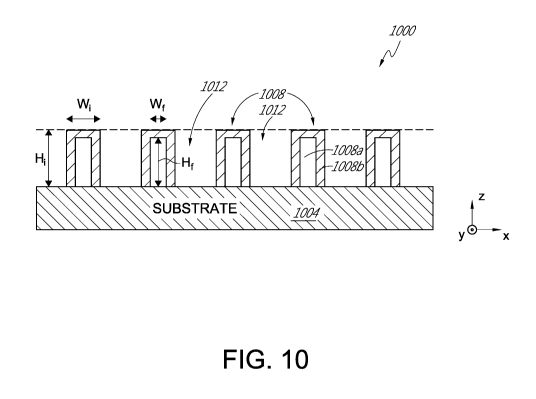
100251 Figure 10 schematically illustrates a cross-sectional view of an
optical
element comprising periodically repeating polymer-based optical structures
having
incorporated therein an inorganic material.
[0026] Figure 11 schematically illustrates a method of fabricating an
optical
element comprising periodically repeating polymer-based optical structures
having
incorporated therein an inorganic material.
-5-
CA 03085459 2020-06-10
WO 2019/136008 PCT/US2018/068025
100271 Figures 12A-12C are cross-sectional views of intermediate
structures at
various stages of providing, using a photolithographic process, periodically
repeating base
polymer structures.
100281 Figures 13A-13C are cross-sectional views of intermediate
structures at
various stages of fabrication using a nanoimprinting process, periodically
repeating base
polymer structures.
100291 Figures 14A-14B are cross-sectional views of intermediate
structures at
various stages of fabrication of an optical element comprising periodically
repeating
polymer-based optical structures having incorporated therein an inorganic
material.
100301 Figures 15A-15B are cross-sectional views of intermediate
structures at
various stages of fabrication of an optical element comprising periodically
repeating
polymer-based optical structures having incorporated therein an inorganic
material.
100311 Figures 16A-16B are cross-sectional views of intermediate
structures at
various stages of fabrication of an optical element comprising periodically
repeating
polymer-based optical structures having incorporated therein an inorganic
material.
100321 Figures 17A-17H illustrate an optical element comprising a
plurality of
waveplate elements, where each waveplate element comprises a pattern of
periodically
repeating polymer-based optical structures having incorporated therein an
inorganic material,
with respect to changes in polarization vectors of an incident light
corresponding to rotations
in the fast axes of the waveplate elements by an angle 0 of 0, 7c/4, 7c/2,
37c/4, it, 57c/4, 37c/2 and
77c/4, respectively.
100331 Figure 18A illustrates a cross-sectional side view of a
diffraction grating
having 2-phase level geometric phase optical elements formed of polymer-based
optical
structures having incorporated therein an inorganic material.
100341 Figure 18B illustrates a top-down view of the diffraction rating
of Figure
18A.
100351 Figure 19 illustrates a top-down view of a diffraction grating
having 4-
phase level geometric phase optical elements formed of polymer-based optical
structures
having incorporated therein an inorganic material.
-6-
CA 03085459 2020-06-10
WO 2019/136008 PCT/US2018/068025
DETAILED DESCRIPTION
100361 Optical systems, such as display systems, often utilize optical
elements to
control the propagation of light. In some applications, due to demand for
compact optical
systems, optical elements having reduced dimensions (e.g., thin structures)
can be useful.
Such optical elements may include, for example, diffractive optical elements.
100371 An example diffractive optical element is a diffractive grating
for coupling
light into a light guide, e.g., a waveguide. The light guide may have, for
example, disposed
thereon or therein, a diffraction grating configured to couple light incident
on the light guide,
e.g., at normal incidence, into the light guide at an angle such that the
diffracted light is
guided within the light guide by total internal reflection. A diffractive
optical element such
as a diffraction grating may be included in or on the light guide to couple
light guided within
the light guide by total internal reflection out of the light guide. A
diffractive optical element
may also be used to manipulate, e.g., redirect and/or modify the beam of light
propagating
within the light guide by total internal reflection. Methods such as described
herein for
fabricating such diffractive optical elements that also provide increased
confinement of light
within the light guides and/or increase diffraction efficiency can be useful.
[0038] Such diffractive optical elements may comprise a pattern of
periodically
repeating optical structures formed on a substrate and configured to diffract
visible light,
where the optical structures have a refractive index greater than the
refractive index of the
substrate. The diffractive optical elements are formed of a polymeric material
having
incorporated therein an inorganic material. The polymeric material in some
cases can serve a
photoresist which remains as final optical structures, and can significantly
reduce fabrication
complexity. Incorporation of the inorganic material in the optical structures
potentially
allows for versatile tuning of optical properties, e.g., refractive index, and
mechanical
properties, e.g., stiffness. The inorganic material can be incorporated using
atomic layer
deposition, which can enable precise control of the amount and depth of
incorporation in the
optical structures.
[0039] Another approach to provide compact optical elements includes
using thin
films, e.g., diffraction gratings based on metasurfaces formed of thin film-
based
nanostructures. Metasurfaces, or metamaterial surfaces, provide opportunities
to realize
virtually flat, aberration-free optics on much smaller scales, in comparison
with geometrical
-7-
CA 03085459 2020-06-10
WO 2019/136008 PCT/US2018/068025
optics. Without being limited by theory, in some embodiments, metasurfaces
include dense
arrangements of surface structures that function as resonant optical antennas.
The resonant
nature of the light-surface structure interaction provides the ability to
manipulate optical
wave-fronts. In some cases, the metasurfaces may allow the replacement of
bulky or difficult
to manufacture optical components with thin, relatively planar elements formed
by simple
patterning processes. However, fabrication of thin film-based optical elements
may include
patterning metals or high-index dielectric materials by lithographically or
nanoimprinting,
both of which can be expensive and/or difficult to implement for structures
having small
dimensions and/or complex shapes.
100401 Advantageously, the polymer-based optical structures having
inorganic
material incorporated therein can be configured as metasurfaces for forming
various optical
elements, including diffractive gratings. The metasurfaces may take the form
of a grating
formed by a plurality of repeating unit cells. Each unit cell may comprise two
sets or more
of nanobeams elongated in crossing directions: one or more first nanobeams
elongated in a
first direction and a plurality of second nanobeams elongated in a second
direction different
from the first direction.
100411 Some diffractive optical elements, e.g., diffractive optical
elements
including metasurfaces formed of the polymer-based optical structures may be
utilized in
wearable display systems to provide compact optical elements. Augmented
reality systems
may display virtual content to a user, or viewer, while still allowing the
user to see the world
around them. This content can be displayed on a head-mounted display, which
may be
mounted on the head of a viewer. The head-mounted display may, for example, be
part of
eyewear, and project image information to the user's eyes. In addition, the
display may also
transmit light from the surrounding environment to the user's eyes, to allow a
view of that
surrounding environment.
100421 Reference will now be made to the drawings, in which like
reference
numerals refer to like parts throughout.
Example Display Systems
100431 Figure 2 illustrates an example of wearable display system 60.
The
display system 60 includes a display 70, and various mechanical and electronic
modules and
-8-
CA 03085459 2020-06-10
WO 2019/136008 PCT/US2018/068025
systems to support the functioning of that display 70. The display 70 may be
coupled to a
frame 80, which is wearable by a display system user or viewer 90 and which is
configured
to position the display 70 in front of the eyes of the user 90. The display 70
may be
considered eyewear in some embodiments. In some embodiments, a speaker 100 is
coupled
to the frame 80 and configured to be positioned adjacent the ear canal of the
user 90 (in some
embodiments, another speaker, not shown, may optionally be positioned adjacent
the other
ear canal of the user to provide stereo/shapeable sound control). The display
system may
also include one or more microphones 110 or other devices to detect sound. In
some
embodiments, the microphone is configured to allow the user to provide inputs
or commands
to the system 60 (e.g., the selection of voice menu commands, natural language
questions,
etc.), and/or may allow audio communication with other persons (e.g., with
other users of
similar display systems. The microphone may further be configured as a
peripheral sensor to
collect audio data (e.g., sounds from the user and/or environment). In some
embodiments,
the display system may also include a peripheral sensor I20a, which may be
separate from
the frame 80 and attached to the body of the user 90 (e.g., on the head,
torso, an extremity,
etc. of the user 90). The peripheral sensor 120a may be configured to acquire
data
characterizing a physiological state of the user 90 in some embodiments. For
example, the
sensor 120a may be an electrode.
[0044] With continued reference to Figure 2, the display 70 is
operatively coupled
by communications link 130, such as by a wired lead or wireless connectivity,
to a local data
processing module 140 which may be mounted in a variety of configurations,
such as fixedly
attached to the frame 80, fixedly attached to a helmet or hat worn by the
user, embedded in
headphones, or otherwise removably attached to the user 90 (e.g., in a
backpack-style
configuration, in a belt-coupling style configuration). Similarly, the sensor
120a may be
operatively coupled by communications link 120b, e.g., a wired lead or
wireless connectivity,
to the local processor and data module 140. The local processing and data
module 140 may
comprise a hardware processor, as well as digital memory, such as non-volatile
memory
(e.g., flash memory or hard disk drives), both of which may be utilized to
assist in the
processing, caching, and storage of data. The data include data a) captured
from sensors
(which may be, e.g., operatively coupled to the frame 80 or otherwise attached
to the user
90), such as image capture devices (such as cameras), microphones, inertial
measurement
-9-
CA 03085459 2020-06-10
WO 2019/136008 PCT/US2018/068025
units, accelerometers, compasses, GPS units, radio devices, gyros, and/or
other sensors
disclosed herein; and/or b) acquired and/or processed using remote processing
module 150
and/or remote data repository 160 (including data relating to virtual
content), possibly for
passage to the display 70 after such processing or retrieval. The local
processing and data
module 140 may be operatively coupled by communication links 170, 180, such as
via a
wired or wireless communication links, to the remote processing module 150 and
remote data
repository 160 such that these remote modules 150, 160 are operatively coupled
to each other
and available as resources to the local processing and data module 140. In
some
embodiments, the local processing and data module 140 may include one or more
of the
image capture devices, microphones, inertial measurement units,
accelerometers, compasses,
GPS units, radio devices, and/or gyros. In some other embodiments, one or more
of these
sensors may be attached to the frame 80, or may be standalone structures that
communicate
with the local processing and data module 140 by wired or wireless
communication
pathways.
100451 With continued reference to Figure 2, in some embodiments, the
remote
processing module 150 may comprise one or more processors configured to
analyze and
process data and/or image information. In some embodiments, the remote data
repository
160 may comprise a digital data storage facility, which may be available
through the internet
or other networking configuration in a "cloud" resource configuration. In some
embodiments, the remote data repository 160 may include one or more remote
servers, which
provide information, e.g., information for generating augmented reality
content, to the local
processing and data module 140 and/or the remote processing module 150. In
some
embodiments, all data is stored and all computations are performed in the
local processing
and data module, allowing fully autonomous use from a remote module.
100461 With reference now to Figure 3, the perception of an image as
being
"three-dimensional" or "3-D" may be achieved by providing slightly different
presentations
of the image to each eye of the viewer. Figure 3 illustrates a conventional
display system for
simulating three-dimensional imagery for a user. Two distinct images 190, 200--
one for
each eye 210, 220¨are outputted to the user. The images 190, 200 are spaced
from the eyes
210, 220 by a distance 230 along an optical or z-axis that is parallel to the
line of sight of the
viewer. The images 190, 200 are flat and the eyes 210, 220 may focus on the
images by
-10-
CA 03085459 2020-06-10
WO 2019/136008 PCT/US2018/068025
assuming a single accommodated state. Such 3-D display systems rely on the
human visual
system to combine the images 190, 200 to provide a perception of depth and/or
scale for the
combined image.
100471 It will be appreciated, however, that the human visual system is
more
complicated and providing a realistic perception of depth is more challenging.
For example,
many viewers of conventional "3-D" display systems find such systems to be
uncomfortable
or may not perceive a sense of depth at all. Without being limited by theory,
it is believed
that viewers of an object may perceive the object as being "three-dimensional"
due to a
combination of vergence and accommodation. Vergence movements (i.e., rotation
of the
eyes so that the pupils move toward or away from each other to converge the
lines of sight of
the eyes to fixate upon an object) of the two eyes relative to each other are
closely associated
with focusing (or "accommodation") of the lenses and pupils of the eyes. Under
normal
conditions, changing the focus of the lenses of the eyes, or accommodating the
eyes, to
change focus from one object to another object at a different distance will
automatically
cause a matching change in vergence to the same distance, under a relationship
known as the
"accommodation-vergence reflex," as well as pupil dilation or constriction.
Likewise, a
change in vergence will trigger a matching change in accommodation of lens
shape and pupil
size, under normal conditions. As noted herein, many stereoscopic or "3-D"
display systems
display a scene using slightly different presentations (and, so, slightly
different images) to
each eye such that a three-dimensional perspective is perceived by the human
visual system.
Such systems are uncomfortable for many viewers, however, since they, among
other things,
simply provide different presentations of a scene, but with the eyes viewing
all the image
information at a single accommodated state, and work against the
"accommodation-vergence
reflex." Display systems that provide a better match between accommodation and
vergence
may form more realistic and comfortable simulations of three-dimensional
imagery.
100481 Figure 4 illustrates aspects of an approach for simulating three-
dimensional imagery using multiple depth planes. =With reference to Figure 4,
objects at
various distances from eyes 210, 220 on the z-axis are accommodated by the
eyes 210, 220
so that those objects are in focus. The eyes 210, 220 assume particular
accommodated states
to bring into focus objects at different distances along the z-axis.
Consequently, a particular
accommodated state may be said to be associated with a particular one of depth
planes 240,
-11-
CA 03085459 2020-06-10
WO 2019/136008 PCT/US2018/068025
with has an associated focal distance, such that objects or parts of objects
in a particular
depth plane are in focus when the eye is in the accommodated state for that
depth plane. In
some embodiments, three-dimensional imagery may be simulated by providing
different
presentations of an image for each of the eyes 210, 220, and also by providing
different
presentations of the image corresponding to each of the depth planes. While
shown as being
separate for clarity of illustration, it will be appreciated that the fields
of view of the eyes
210, 220 may overlap, for example, as distance along the z-axis increases. In
addition, while
shown as flat for ease of illustration, it will be appreciated that the
contours of a depth plane
may be curved in physical space, such that all features in a depth plane are
in focus with the
eye in a particular accommodated state.
100491 The distance between an object and the eye 210 or 220 may also
change
the amount of divergence of light from that object, as viewed by that eye.
Figures 5A-5C
illustrate relationships between distance and the divergence of light rays.
The distance
between the object and the eye 210 is represented by, in order of decreasing
distance, R1, R2,
and R3. As shown in Figures 5A-5C, the light rays become more divergent as
distance to the
object decreases. As distance increases, the light rays become more
collimated. Stated
another way, it may be said that the light field produced by a point (the
object or a part of the
object) has a spherical wavefront curvature, which is a function of how far
away the point is
from the eye of the user. The curvature increases with decreasing distance
between the
object and the eye 210. Consequently, at different depth planes, the degree of
divergence of
light rays is also different, with the degree of divergence increasing with
decreasing distance
between depth planes and the viewer's eye 210. While only a single eye 210 is
illustrated for
clarity of illustration in Figures 5A-5C and other figures herein, it will be
appreciated that the
discussions regarding eye 210 may be applied to both eyes 210 and 220 of a
viewer.
100501 Without being limited by theory, it is believed that the human
eye
typically can interpret a finite number of depth planes to provide depth
perception.
Consequently, a highly believable simulation of perceived depth may be
achieved by
providing, to the eye, different presentations of an image corresponding to
each of these
limited number of depth planes. The different presentations may be separately
focused by
the viewer's eyes, thereby helping to provide the user with depth cues based
on the
accommodation of the eye required to bring into focus different image features
for the scene
-12-
CA 03085459 2020-06-10
WO 2019/136008 PCT/US2018/068025
located on different depth plane and/or based on observing different image
features on
different depth planes being out of focus.
100511 Figure 6 illustrates an example of a waveguide stack for
outputting image
information to a user. A display system 250 includes a stack of waveguides, or
stacked
waveguide assembly, 260 that may be utilized to provide three-dimensional
perception to the
eye/brain using a plurality of waveguides 270, 280, 290, 300, 310. In some
embodiments,
the display system 250 is the system 60 of Figure 2, with Figure 6
schematically showing
some parts of that system 60 in greater detail. For example, the waveguide
assembly 260
may be part of the display 70 of Figure 2. It will be appreciated that the
display system 250
may be considered a light field display in some embodiments.
100521 With continued reference to Figure 6, the waveguide assembly 260
may
also include a plurality of features 320, 330, 340, 350 between the
waveguides. In some
embodiments, the features 320, 330, 340, 350 may be one or more lenses. The
waveguides
270, 280, 290, 300, 310 and/or the plurality of lenses 320, 330, 340, 350 may
be configured
to send image information to the eye with various levels of wavefront
curvature or light ray
divergence. Each waveguide level may be associated with a particular depth
plane and may
be configured to output image information corresponding to that depth plane.
Image
injection devices 360, 370, 380, 390, 400 may function as a source of light
for the
waveguides and may be utilized to inject image information into the waveguides
270, 280,
290, 300, 310, each of which may be configured, as described herein, to
distribute incoming
light across each respective waveguide, for output toward the eye 210. Light
exits an output
surface 410, 420, 430, 440, 450 of the image injection devices 360, 370, 380,
390, 400 and is
injected into a corresponding input surface 460, 470, 480, 490, 500 of the
waveguides 270,
280, 290, 300, 310. In some embodiments, the each of the input surfaces 460,
470, 480, 490,
500 may be an edge of a corresponding waveguide, or may be part of a major
surface of the
corresponding waveguide (that is, one of the waveguide surfaces directly
facing the world
510 or the viewer's eye 210). In some embodiments, a single beam of light
(e.g. a collimated
beam) may be injected into each waveguide to output an entire field of cloned
collimated
beams that are directed toward the eye 210 at particular angles (and amounts
of divergence)
corresponding to the depth plane associated with a particular waveguide. In
some
embodiments, a single one of the image injection devices 360, 370, 380, 390,
400 may be
-13-
CA 03085459 2020-06-10
WO 2019/136008 PCT/US2018/068025
associated with and inject light into a plurality (e.g., three) of the
waveguides 270, 280, 290,
300, 310.
100531 In some embodiments, the image injection devices 360, 370, 380,
390, 400
are discrete displays that each produce image information for injection into a
corresponding
waveguide 270, 280, 290, 300, 310, respectively. In some other embodiments,
the image
injection devices 360, 370, 380, 390, 400 are the output ends of a single
multiplexed display
which may, e.g., pipe image information via one or more optical conduits (such
as fiber optic
cables) to each of the image injection devices 360, 370, 380, 390, 400. It
will be appreciated
that the image information provided by the image injection devices 360, 370,
380, 390, 400
may include light of different wavelengths, or colors (e.g., different
component colors, as
discussed herein).
100541 In some embodiments, the light injected into the waveguides 270,
280,
290, 300, 310 is provided by a light projector system 520, which comprises a
light module
530, which may include a light emitter, such as a light emitting diode (LED).
The light from
the light module 530 may be directed to and modified by a light modulator 540,
e.g., a spatial
light modulator, via a beam splitter 550. The light modulator 540 may be
configured to
change the perceived intensity of the light injected into the waveguides 270,
280, 290, 300,
310. Examples of spatial light modulators include liquid crystal displays
(LCD) including a
liquid crystal on silicon (LCOS) displays.
100551 In some embodiments, the display system 250 may be a scanning
fiber
display comprising one or more scanning fibers configured to project light in
various patterns
(e.g., raster scan, spiral scan, Lissajous patterns, etc.) into one or more
waveguides 270, 280,
290, 300, 310 and ultimately to the eye 210 of the viewer. in some
embodiments, the
illustrated image injection devices 360, 370, 380, 390, 400 may schematically
represent a
single scanning fiber or a bundle of scanning fibers configured to inject
light into one or a
plurality of the waveguides 270, 280, 290, 300, 310. In some other
embodiments, the
illustrated image injection devices 360, 370, 380, 390, 400 may schematically
represent a
plurality of scanning fibers or a plurality of bundles of scanning fibers,
each of which are
configured to inject light into an associated one of the waveguides 270, 280,
290, 300, 310.
It will be appreciated that one or more optical fibers may be configured to
transmit light from
the light module 530 to the one or more waveguides 270, 280, 290, 300, 310. It
will be
-14-
CA 03085459 2020-06-10
WO 2019/136008 PCT/US2018/068025
appreciated that one or more intervening optical structures may be provided
between the
scanning fiber, or fibers, and the one or more waveguides 270, 280, 290, 300,
310 to, e.g.,
redirect light exiting the scanning fiber into the one or more waveguides 270,
280, 290, 300,
310.
100561 A controller 560 controls the operation of one or more of the
stacked
waveguide assembly 260, including operation of the image injection devices
360, 370, 380,
390, 400, the light source 530, and the light modulator 540. In some
embodiments, the
controller 560 is part of the local data processing module 140. The controller
560 includes
programming (e.g., instructions in a non-transitory medium) that regulates the
timing and
provision of image information to the waveguides 270, 280, 290, 300, 310
according to, e.g.,
any of the various schemes disclosed herein. In some embodiments, the
controller may be a
single integral device, or a distributed system connected by wired or wireless
communication
channels. The controller 560 may be part of the processing modules 140 or 150
(Figure 2) in
some embodiments.
100571 With continued reference to Figure 6, the waveguides 270, 280,
290, 300,
310 may be configured to propagate light within each respective waveguide by
total internal
reflection (TIR). The waveguides 270, 280, 290, 300, 310 may each be planar or
have
another shape (e.g., curved), with major top and bottom surfaces and edges
extending
between those major top and bottom surfaces. In the illustrated configuration,
the
waveguides 270, 280, 290, 300, 310 may each include out-coupling optical
elements 570,
580, 590, 600, 610 that are configured to extract light out of a waveguide by
redirecting the
light, propagating within each respective waveguide, out of the waveguide to
output image
information to the eye 210. Extracted light may also be referred to as out-
coupled light and
the out-coupling optical elements light may also be referred to light
extracting optical
elements. An extracted beam of light may be outputted by the waveguide at
locations at
which the light propagating in the waveguide strikes a light extracting
optical element. I'he
out-coupling optical elements 570, 580, 590, 600, 610 may, for example, be
gratings,
including diffractive optical features, as discussed further herein. While
illustrated disposed
at the bottom major surfaces of the waveguides 270, 280, 290, 300, 310, for
ease of
description and drawing clarity, in some embodiments, the out-coupling optical
elements
570, 580, 590, 600,610 may be disposed at the top and/or bottom major
surfaces, and/or may
-15-
CA 03085459 2020-06-10
WO 2019/136008 PCT/US2018/068025
be disposed directly in the volume of the waveguides 270, 280, 290, 300, 310,
as discussed
further herein. In some embodiments, the out-coupling optical elements 570,
580, 590, 600,
610 may be formed in a layer of material that is attached to a transparent
substrate to form
the waveguides 270, 280, 290, 300, 310. In some other embodiments, the
waveguides 270,
280, 290, 300, 310 may be a monolithic piece of material and the out-coupling
optical
elements 570, 580, 590, 600, 610 may be formed on a surface and/or in the
interior of that
piece of material.
100581 With continued reference to Figure 6, as discussed herein, each
waveguide
270, 280, 290, 300, 310 is configured to output light to form an image
corresponding to a
particular depth plane. For example, the waveguide 270 nearest the eye may be
configured
to deliver collimated light (which was injected into such waveguide 270), to
the eye 210.
The collimated light may be representative of the optical infinity focal
plane. The next
waveguide up 280 may be configured to send out collimated light which passes
through the
first lens 350 (e.g., a negative lens) before it can reach the eye 210; such
first lens 350 may
be configured to create a slight convex wavefront curvature so that the
eye/brain interprets
light coming from that next waveguide up 280 as coming from a first focal
plane closer
inward toward the eye 210 from optical infinity. Similarly, the third up
waveguide 290
passes its output light through both the first 350 and second 340 lenses
before reaching the
eye 210; the combined optical power of the first 350 and second 340 lenses may
be
configured to create another incremental amount of wavefront curvature so that
the eye/brain
interprets light coming from the third waveguide 290 as coming from a second
focal plane
that is even closer inward toward the person from optical infinity than was
light from the next
waveguide up 280.
100591 The other waveguide layers 300, 310 and lenses 330, 320 are
similarly
configured, with the highest waveguide 310 in the stack sending its output
through all of the
lenses between it and the eye for an aggregate focal power representative of
the closest focal
plane to the person. To compensate for the stack of lenses 320, 330, 340, 350
when
viewing/interpreting light coming from the world 510 on the other side of the
stacked
waveguide assembly 260, a compensating lens layer 620 may be disposed at the
top of the
stack to compensate for the aggregate power of the lens stack 320, 330, 340,
350 below.
Such a configuration provides as many perceived focal planes as there are
available
-16-
CA 03085459 2020-06-10
WO 2019/136008 PCT/US2018/068025
waveguide/lens pairings. Both the out-coupling optical elements of the
waveguides and the
focusing aspects of the lenses may be static (i.e., not dynamic or electro-
active). In some
alternative embodiments, either or both may be dynamic using electro-active
features.
100601 In some embodiments, two or more of the waveguides 270, 280,
290, 300,
310 may have the same associated depth plane. For example, multiple waveguides
270, 280,
290, 300, 310 may be configured to output images set to the same depth plane,
or multiple
subsets of the waveguides 270, 280, 290, 300, 310 may be configured to output
images set to
the same plurality of depth planes, with one set for each depth plane. This
can provide
advantages for forming a tiled image to provide an expanded field of view at
those depth
planes.
[00611 With continued reference to Figure 6, the out-coupling optical
elements
570, 580, 590, 600, 610 may be configured to both redirect light out of their
respective
waveguides and to output this light with the appropriate amount of divergence
or collimation
for a particular depth plane associated with the waveguide. As a result,
waveguides having
different associated depth planes may have different configurations of out-
coupling optical
elements 570, 580, 590, 600, 610, which output light with a different amount
of divergence
depending on the associated depth plane. In some embodiments, the light
extracting optical
elements 570, 580, 590, 600, 610 may be volumetric or surface features, which
may be
configured to output light at specific angles. For example, the light
extracting optical
elements 570, 580, 590, 600, 610 may be volume holograms, surface holograms,
and/or
diffraction gratings. In some embodiments, the features 320, 330, 340, 350 may
not be
lenses; rather, they may simply be spacers (e.g., cladding layers and/or
structures for forming
air gaps).
100621 In some embodiments, the out-coupling optical elements 570, 580,
590,
600, 610 are diffractive features that form a diffraction pattern, or
"diffractive optical
element" (also referred to herein as a "DOE"). Preferably, the DOE's have a
sufficiently low
diffraction efficiency so that only a portion of the light of the beam is
deflected away toward
the eye 210 with each intersection of the DOE, while the rest continues to
move through a
waveguide via TIR. The light carrying the image information is thus divided
into a number
of related exit beams that exit the waveguide at a multiplicity of locations
and the result is a
-17-
CA 03085459 2020-06-10
WO 2019/136008 PCT/US2018/068025
fairly uniform pattern of exit emission toward the eye 210 for this particular
collimated beam
bouncing around within a waveguide.
100631 In some embodiments, one or more DOEs may be switchable between
"on" states in which they actively diffract, and "off' states in which they do
not significantly
diffract. For instance, a switchable DOE may comprise a layer of polymer
dispersed liquid
crystal, in which microdroplets comprise a diffraction pattern in a host
medium, and the
refractive index of the microdroplets may be switched to substantially match
the refractive
index of the host material (in which case the pattern does not appreciably
diffract incident
light) or the microdroplet may be switched to an index that does not match
that of the host
medium (in which case the pattern actively diffracts incident light).
100641 In some embodiments, a camera assembly 630 (e.g., a digital
camera,
including visible light and infrared light cameras) may be provided to capture
images of the
eye 210 and/or tissue around the eye 210 to, e.g., detect user inputs and/or
to monitor the
physiological state of the user. As used herein, a camera may be any image
capture device.
In some embodiments, the camera assembly 630 may include an image capture
device and a
light source to project light (e.g., infrared light) to the eye, which may
then be reflected by
the eye and detected by the image capture device. In some embodiments, the
camera
assembly 630 may be attached to the frame 80 (Figure 2) and may be in
electrical
communication with the processing modules 140 and/or 150, which may process
image
information from the camera assembly 630. In some embodiments, one camera
assembly
630 may be utilized for each eye, to separately monitor each eye.
100651 With reference now to Figure 7, an example of exit beams
outputted by a
waveguide is shown. One waveguide is illustrated, but it will be appreciated
that other
waveguides in the waveguide assembly 260 (Figure 6) may function similarly,
where the
waveguide assembly 260 includes multiple waveguides. Light 640 is injected
into the
waveguide 270 at the input surface 460 of the waveguide 270 and propagates
within the
waveguide 270 by TIR. At points where the light 640 impinges on the DOE 570, a
portion of
the light exits the waveguide as exit beams 650. The exit beams 650 are
illustrated as
substantially parallel but, as discussed herein, they may also be redirected
to propagate to the
eye 210 at an angle (e.g., forming divergent exit beams), depending on the
depth plane
associated with the waveguide 270. It will be appreciated that substantially
parallel exit
-18-
CA 03085459 2020-06-10
WO 2019/136008 PCT/US2018/068025
beams may be indicative of a waveguide with out-coupling optical elements that
out-couple
light to form images that appear to be set on a depth plane at a large
distance (e.g., optical
infinity) from the eye 210. Other waveguides or other sets of out-coupling
optical elements
may output an exit beam pattern that is more divergent, which would require
the eye 210 to
accommodate to a closer distance to bring it into focus on the retina and
would be interpreted
by the brain as light from a distance closer to the eye 210 than optical
infinity.
100661 In some embodiments, a full color image may be formed at each
depth
plane by overlaying images in each of the component colors, e.g., three or
more component
colors. Figure 8 illustrates an example of a stacked waveguide assembly in
which each depth
plane includes images formed using multiple different component colors. The
illustrated
embodiment shows depth planes 240a ¨ 240f, although more or fewer depths are
also
contemplated. Each depth plane may have three or more component color images
associated
with it, including: a first image of a first color, G; a second image of a
second color, R; and a
third image of a third color, B. Different depth planes are indicated in the
figure by different
numbers for diopters (dpt) following the letters G, R, and B. Just as
examples, the numbers
following each of these letters indicate diopters (1/m), or inverse distance
of the depth plane
from a viewer, and each box in the figures represents an individual component
color image.
In some embodiments, to account for differences in the eye's focusing of light
of different
wavelengths, the exact placement of the depth planes for different component
colors may
vary. For example, different component color images for a given depth plane
may be placed
on depth planes corresponding to different distances from the user. Such an
arrangement
may increase visual acuity and user comfort and/or may decrease chromatic
aberrations.
100671 In some embodiments, light of each component color may be
outputted by
a single dedicated waveguide and, consequently, each depth plane may have
multiple
waveguides associated with it. In such embodiments, each box in the figures
including the
letters G, R, or B may be understood to represent an individual waveguide, and
three
waveguides may be provided per depth plane where three component color images
are
provided per depth plane. While the waveguides associated with each depth
plane are shown
adjacent to one another in this drawing for ease of description, it will be
appreciated that, in a
physical device, the waveguides may all be arranged in a stack with one
waveguide per level.
-19-
CA 03085459 2020-06-10
WO 2019/136008 PCT/US2018/068025
In some other embodiments, multiple component colors may be outputted by the
same
waveguide, such that, e.g., only a single waveguide may be provided per depth
plane.
100681 With continued reference to Figure 8, in some embodiments, G is
the color
green, R is the color red, and B is the color blue. In some other embodiments,
other colors
associated with other wavelengths of light, including magenta and cyan, may be
used in
addition to or may replace one or more of red, green, or blue.
100691 It will be appreciated that references to a given color of light
throughout
this disclosure will be understood to encompass light of one or more
wavelengths within a
range of wavelengths of light that are perceived by a viewer as being of that
given color. For
example, red light may include light of one or more wavelengths in the range
of about 620-
780 nm, green light may include light of one or more wavelengths in the range
of about 492-
577 nm, and blue light may include light of one or more wavelengths in the
range of about
435-493 nm.
100701 In some embodiments, the light source 530 (Figure 6) may be
configured
to emit light of one or more wavelengths outside the visual perception range
of the viewer,
for example, infrared and/or ultraviolet wavelengths. In addition, the in-
coupling, out-
coupling, and other light redirecting structures of the waveguides of the
display 250 may be
configured to direct and emit this light out of the display towards the user's
eye 210, e.g., for
imaging and/or user stimulation applications.
100711 With reference now to Figure 9A, in some embodiments, light
impinging
on a waveguide may need to be redirected to in-couple that light into the
waveguide. An in-
coupling optical element may be used to redirect and in-couple the light into
its
corresponding waveguide. Figure 9A illustrates a cross-sectional side view of
an example of
a plurality or set 660 of stacked waveguides that each includes an in-coupling
optical
element. The waveguides may each be configured to output light of one or more
different
wavelengths, or one or more different ranges of wavelengths. It will be
appreciated that the
stack 660 may correspond to the stack 260 (Figure 6) and the illustrated
waveguides of the
stack 660 may correspond to part of the plurality of waveguides 270, 280, 290,
300, 310,
except that light from one or more of the image injection devices 360, 370,
380, 390, 400 is
injected into the waveguides from a position that requires light to be
redirected for in-
coupling.
-20-
CA 03085459 2020-06-10
WO 2019/136008 PCT/US2018/068025
100721 The illustrated set 660 of stacked waveguides includes
waveguides 670,
680, and 690. Each waveguide includes an associated in-coupling optical
element (which
may also be referred to as a light input area on the waveguide), with, e.g.,
in-coupling optical
element 700 disposed on a major surface (e.g., an upper major surface) of
waveguide 670, in-
coupling optical element 710 disposed on a major surface (e.g., an upper major
surface) of
waveguide 680, and in-coupling optical element 720 disposed on a major surface
(e.g., an
upper major surface) of waveguide 690. In some embodiments, one or more of the
in-
coupling optical elements 700, 710, 720 may be disposed on the bottom major
surface of the
respective waveguide 670, 680, 690 (particularly where the one or more in-
coupling optical
elements are reflective, deflecting optical elements). As illustrated, the in-
coupling optical
elements 700, 710, 720 may be disposed on the upper major surface of their
respective
waveguide 670, 680, 690 (or the top of the next lower waveguide), particularly
where those
in-coupling optical elements are transmissive, deflecting optical elements. In
some
embodiments, the in-coupling optical elements 700, 710, 720 may be disposed in
the body of
the respective waveguide 670, 680, 690. In some embodiments, as discussed
herein, the in-
coupling optical elements 700, 710, 720 are wavelength selective, such that
they selectively
redirect one or more wavelengths of light, while transmitting other
wavelengths of light.
While illustrated on one side or corner of their respective waveguide 670,
680, 690, it will be
appreciated that the in-coupling optical elements 700, 710, 720 may be
disposed in other
areas of their respective waveguide 670, 680, 690 in some embodiments.
100731 As illustrated, the in-coupling optical elements 700, 710, 720
may be
laterally offset from one another. In some embodiments, each in-coupling
optical element
may be offset such that it receives light without that light passing through
another in-
coupling optical element. For example, each in-coupling optical element 700,
710, 720 may
be configured to receive light from a different image injection device 360,
370, 380, 390, and
400 as shown in Figure 6, and may be separated (e.g., laterally spaced apart)
from other in-
coupling optical elements 700, 710, 720 such that it substantially does not
receive light from
the other ones of the in-coupling optical elements 700, 710, 720.
100741 Each waveguide also includes associated light distributing
elements, with,
e.g., light distributing elements 730 disposed on a major surface (e.g., a top
major surface) of
waveguide 670, light distributing elements 740 disposed on a major surface
(e.g., a top major
-21-
CA 03085459 2020-06-10
WO 2019/136008 PCT/US2018/068025
surface) of waveguide 680, and light distributing elements 750 disposed on a
major surface
(e.g., a top major surface) of waveguide 690. In some other embodiments, the
light
distributing elements 730, 740, 750, may be disposed on a bottom major surface
of
associated waveguides 670, 680, 690, respectively. In some other embodiments,
the light
distributing elements 730, 740, 750, may be disposed on both top and bottom
major surface
of associated waveguides 670, 680, 690, respectively; or the light
distributing elements 730,
740, 750, may be disposed on different ones of the top and bottom major
surfaces in different
associated waveguides 670, 680, 690, respectively.
100751 The waveguides 670, 680, 690 may be spaced apart and separated
by, e.g.,
gas, liquid, and/or solid layers of material. For example, as illustrated,
layer 760a may
separate waveguides 670 and 680; and layer 760b may separate waveguides 680
and 690. In
some embodiments, the layers 760a and 760b are formed of low refractive index
materials
(that is, materials having a lower refractive index than the material forming
the immediately
adjacent one of waveguides 670, 680, 690). Preferably, the refractive index of
the material
forming the layers 760a, 760b is 0.05 or more, or 0.10 or less than the
refractive index of the
material forming the waveguides 670, 680, 690. Advantageously, the lower
refractive index
layers 760a, 760b may function as cladding layers that facilitate total
internal reflection (TIR)
of light through the waveguides 670, 680, 690 (e.g., TIR between the top and
bottom major
surfaces of each waveguide). In some embodiments, the layers 760a, 760b are
formed of air.
While not illustrated, it will be appreciated that the top and bottom of the
illustrated set 660
of waveguides may include immediately neighboring cladding layers.
100761 Preferably, for ease of manufacturing and other considerations,
the
material forming the waveguides 670, 680, 690 are similar or the same, and the
material
forming the layers 760a, 760b are similar or the same. In some embodiments,
the material
forming the waveguides 670, 680, 690 may be different between one or more
waveguides,
and/or the material forming the layers 760a, 760b may be different, while
still holding to the
various refractive index relationships noted above.
100771 With continued reference to Figure 9A, light rays 770, 780, 790
are
incident on the set 660 of waveguides. It will be appreciated that the light
rays 770, 780, 790
may be injected into the waveguides 670, 680, 690 by one or more image
injection devices
360, 370, 380, 390, 400 (Figure 6).
-22-
CA 03085459 2020-06-10
WO 2019/136008 PCT/US2018/068025
100781 In some embodiments, the light rays 770, 780, 790 have different
properties, e.g., different wavelengths or different ranges of wavelengths,
which may
correspond to different colors. The in-coupling optical elements 700, 710, 720
each deflect
the incident light such that the light propagates through a respective one of
the waveguides
670, 680, 690 by TIR. In some embodiments, the incoupling optical elements
700, 710, 720
each selectively deflect one or more particular wavelengths of light, while
transmitting other
wavelengths to an underlying waveguide and associated incoupling optical
element.
100791 For example, in-coupling optical element 700 may be configured
to
deflect ray 770, which has a first wavelength or range of wavelengths, while
transmitting
rays 1242 and 1244, which have different second and third wavelengths or
ranges of
wavelengths, respectively. The transmitted ray 780 impinges on and is
deflected by the in-
coupling optical element 710, which is configured to deflect light of a second
wavelength or
range of wavelengths. The ray 790 is deflected by the in-coupling optical
element 720,
which is configured to selectively deflect light of third wavelength or range
of wavelengths.
100801 With continued reference to Figure 9A, the deflected light rays
770, 780,
790 are deflected so that they propagate through a corresponding waveguide
670, 680, 690;
that is, the in-coupling optical elements 700, 710, 720 of each waveguide
deflects light into
that corresponding waveguide 670, 680, 690 to in-couple light into that
corresponding
waveguide. The light rays 770, 780, 790 are deflected at angles that cause the
light to
propagate through the respective waveguide 670, 680, 690 by TIR. The light
rays 770, 780,
790 propagate through the respective waveguide 670, 680, 690 by TIR until
impinging on the
waveguide's corresponding light distributing elements 730, 740, 750.
100811 With reference now to Figure 9B, a perspective view of an
example of the
plurality of stacked waveguides of Figure 9A is illustrated. As noted above,
the in-coupled
light rays 770, 780, 790, are deflected by the in-coupling optical elements
700, 710, 720,
respectively, and then propagate by T1R within the waveguides 670, 680, 690,
respectively.
The light rays 770, 780, 790 then impinge on the light distributing elements
730, 740, 750,
respectively. The light distributing elements 730, 740, 750 deflect the light
rays 770, 780,
790 so that they propagate towards the out-coupling optical elements 800, 810,
820,
respectively.
-23-
CA 03085459 2020-06-10
WO 2019/136008 PCT/US2018/068025
100821 In some embodiments, the light distributing elements 730, 740,
750 are
orthogonal pupil expanders (OPE's). In some embodiments, the OPE's deflect or
distribute
light to the out-coupling optical elements 800, 810, 820 and, in some
embodiments, may also
increase the beam or spot size of this light as it propagates to the out-
coupling optical
elements. In some embodiments, the light distributing elements 730, 740, 750
may be
omitted and the in-coupling optical elements 700, 710, 720 may be configured
to deflect light
directly to the out-coupling optical elements 800, 810, 820. For example, with
reference to
Figure 9A, the light distributing elements 730, 740, 750 may be replaced with
out-coupling
optical elements 800, 810, 820, respectively. In some embodiments, the out-
coupling optical
elements 800, 810, 820 are exit pupils (EP's) or exit pupil expanders (EPE's)
that direct light
in a viewer's eye 210 (Figure 7). It will be appreciated that the OPE's may be
configured to
increase the dimensions of the eye box in at least one axis and the EPE's may
be to increase
the eye box in an axis crossing, e.g., orthogonal to, the axis of the OPEs.
For example, each
OPE may be configured to redirect a portion of the light striking the OPE to
an EFT of the
same waveguide, while allowing the remaining portion of the light to continue
to propagate
down the waveguide. Upon impinging on the OPE again, another portion of the
remaining
light is redirected to the EPE, and the remaining portion of that portion
continues to
propagate further down the waveguide, and so on. Similarly, upon striking the
EPE, a
portion of the impinging light is directed out of the waveguide towards the
user, and a
remaining portion of that light continues to propagate through the waveguide
until it strikes
the EP again, at which time another portion of the impinging light is directed
out of the
waveguide, and so on. Consequently, a single beam of incoupled light may be
"replicated"
each time a portion of that light is redirected by an OPE or EPE, thereby
forming a field of
cloned beams of light, as shown in Figure 6. In some embodiments, the OPE
and/or EPE
may be configured to modify a size of the beams of light.
100831 Accordingly, with reference to Figures 9A and 9B, in some
embodiments,
the set 660 of waveguides includes waveguides 670, 680, 690; in-coupling
optical elements
700, 710, 720; light distributing elements (e.g., OPE's) 730, 740, 750; and
out-coupling
optical elements (e.g., EP's) 800, 810, 820 for each component color. The
waveguides 670,
680, 690 may be stacked with an air gap/cladding layer between each one. The
in-coupling
optical elements 700, 710, 720 redirect or deflect incident light (with
different in-coupling
-24-
CA 03085459 2020-06-10
WO 2019/136008 PCT/US2018/068025
optical elements receiving light of different wavelengths) into its waveguide.
The light then
propagates at an angle which will result in TIR within the respective
waveguide 670, 680,
690. In the example shown, light ray 770 (e.g., blue light) is deflected by
the first in-
coupling optical element 700, and then continues to bounce down the waveguide,
interacting
with the light distributing element (e.g., OPE's) 730 and then the out-
coupling optical
element (e.g., EPs) 800, in a manner described earlier. The light rays 780 and
790 (e.g.,
green and red light, respectively) will pass through the waveguide 670, with
light ray 780
impinging on and being deflected by in-coupling optical element 710. The light
ray 780 then
bounces down the waveguide 680 via TIR, proceeding on to its light
distributing element
(e.g., OPEs) 740 and then the out-coupling optical element (e.g., EP's) 810.
Finally, light ray
790 (e.g., red light) passes through the waveguide 690 to impinge on the light
in-coupling
optical elements 720 of the waveguide 690. The light in-coupling optical
elements 720
deflect the light ray 790 such that the light ray propagates to light
distributing element (e.g.,
OPEs) 750 by TM, and then to the out-coupling optical element (e.g., EPs) 820
by TIR. The
out-coupling optical element 820 then finally out-couples the light ray 790 to
the viewer,
who also receives the out-coupled light from the other waveguides 670, 680.
100841 Figure 9C illustrates a top-down plan view of an example of the
plurality
of stacked waveguides of Figures 9A and 9B. As illustrated, the waveguides
670, 680, 690,
along with each waveguide's associated light distributing element 730, 740,
750 and
associated out-coupling optical element 800, 810, 820, may be vertically
aligned. However,
as discussed herein, the in-coupling optical elements 700, 710, 720 are not
vertically aligned:
rather, the in-coupling optical elements are preferably non-overlapping (e.g.,
laterally spaced
apart as seen in the top-down view). As discussed further herein, this
nonoverlapping spatial
arrangement facilitates the injection of light from different resources into
different
waveguides on a one-to-one basis, thereby allowing a specific light source to
be uniquely
coupled to a specific waveguide. In some embodiments, arrangements including
nonoverlapping spatially-separated in-coupling optical elements may be
referred to as a
shifted pupil system, and the in-coupling optical elements within these
arrangements may
correspond to sub pupils.
Optical Elements Formed of Polymer-based Optical Structures Incorporating an
Inorganic Material
-25-
CA 03085459 2020-06-10
WO 2019/136008 PCT/US2018/068025
100851 Display systems may employ various optical elements for
controlling the
propagation of light. However, in some contexts, such as display systems
including a head-
mounted display device (e.g., the display system 80 described supra with
reference to Figure
2), conventional optical elements may not be desirable or suitable, owing to
their relatively
heavy weight, large size, manufacturing challenges, and/or deficiencies in
optical properties
such as diffraction angles and diffraction efficiency.
100861 For example, as described above with reference to Figures 9A-9C,
display
systems may include optical elements (e.g., incoupling optical elements, light
distributing
elements and outcoupling optical elements), which may include diffraction
gratings.
Furthermore, as further described above with reference to Figures 9A-9C, light
that is
coupled into a corresponding waveguide can propagate within the waveguide by
total internal
reflection (TIR). To achieve TIR, it may be desirable for the diffraction
grating to have
relatively high diffraction angles relative to a surface normal. In addition,
high diffraction
efficiencies can be desirable to increase light intensity and image
brightness. However,
providing diffraction gratings capable of achieving high diffraction angles
and high
diffraction efficiencies for visible light can impose a challenge. To address
these and other
needs, examples of optical elements disclosed herein, e.g., diffraction
gratings, may utilize
optical elements formed of periodically repeating polymer-based optical
structures which
incorporate therein an inorganic material.
100871 Figure 10 illustrates a cross-sectional view of an optical
element, e.g., a
diffraction grating 1000, comprising periodically repeating polymer-based
optical structures
having incorporated therein an inorganic material, according to various
implementations.
The diffraction grating 1000 includes a substrate 1004 having a first
refractive index (ni) and
transparent in the visible spectrum. The diffraction grating 1000 additionally
includes a
pattern of periodically repeating optical structures 1008 formed on the
substrate 1004 and
configured to diffract visible light. The optical structures 1008 have a
second refractive
index (n2) greater than the first refractive index and comprise a polymeric
material having
incorporated therein an inorganic material.
100881 According to embodiments, the substrate 1004 is transparent in
the visible
spectrum. As described herein and throughout the specification, a
"transmissive" or
-26-
CA 03085459 2020-06-10
WO 2019/136008 PCT/US2018/068025
"transparent" structure, e.g., a transmissive substrate, may allow at least
some, e.g., at least
20, 30, 50, 70, 90%, or 95% of an incident light, to pass therethrough but may
transmit less
than 99% or 100%. The percent transmission may be within any range defined by
any of
these values or may be outside these ranges. Accordingly, a transparent
substrate may be a
glass, sapphire or a polymeric substrate in some embodiments. A "reflective"
structure, e.g.,
a reflective substrate, may reflect at least some, e.g., at least 20, 30, 50,
70, 90%, or 95% or
more of the incident light, to reflect therefrom but may reflect less than 99%
or 100%. The
percent reflection may be within any range defined by any of these values or
may be outside
these ranges.
100891
According to embodiments, the substrate 1004 has a first refractive index
(ni) that is greater that of air but less than the second refractive index n2
of the optical
structures 1008. The n i can have a value, e.g., about 1.5, 1.6, 1.7, 1.8,
1.9, or any value in
any range defined by these values or outside theses ranges. Examples of
materials for
forming the substrate 1004 include silica glass (e.g., doped silica glass),
silicon oxynitride,
transition metal oxides (e.g., hafnium oxide, tantalum oxide, zirconium oxide,
niobium oxide,
lithium niobate, aluminum oxide (e.g., sapphire)), plastic, polymer, or other
optically
transmissive material having, e.g., a suitable refractive index as described
herein.
100901 The
pattern of periodically repeating optical structures 1008 formed on the
substrate 1004 is configured to diffract visible light, due to the material,
dimensions and
geometric configuration, such as described herein.
100911 Still
referring to Figure 10, according to various embodiments, the optical
structures 1008 comprise a base polymeric material having incorporated therein
an inorganic
material. The base polymeric material may comprise a suitable polymer for
incorporation of
the inorganic material and for serving as a material that can be patterned
lithographically
such as a photosensitive material that can be patterned photolithographically
such as
photoresist or another material that can be easily patterned. For example, the
base polymeric
material can include, among other polymers, polyethylene (PE)(¨(CH2-CH2)n¨),
polypropylene (PP)(¨[CH2-CH(CH3)].--), poly(vinyl chloride)(PVC) (¨[CH2-
CH(CH3)]nr-),
poly(vinylidene chloride)(--(CH2-CC12)n¨), polystyrene (PS)(¨[CH2-
CH(C6H5)]n¨),
polyacrylonitrile (PAN)(¨(CH2-CHCN)11), polytetrafluoroethylene (PTFE,)( --
(CF2-CF2)nr-),
poly(methyl methacrylate)(PMMA)(¨[CH2-C(CH3)CO2CH3]n¨),
poly(vinyl
-27-
CA 03085459 2020-06-10
WO 2019/136008 PCT/US2018/068025
acetateXPVAc)(¨(CH2-CHOCOCH3),¨), cis-polyisoprene (-1CH2-CH=C(CH3)-CH2b¨),
and
polychloroprene (cis + trans) (-1CH2-CHC1-CH2],---), to name a few. In some
embodiments, chains of the base polymer may be configured as a homopolymer. In
some
other embodiments, chains of the base polymer may be configured as a
copolymer. When
configured as a copolymer, chains of the base polymer may be configured to
have one of
various forms, including but not limited to, e.g., a statistical copolymer, an
alternating
copolymer, a block copolymer and a graft copolymer incorporating monomer units
of the
various polymers described above.
100921 The specific polymer may be selected based on, among other
factors, the
deposition chemistry for forming the inorganic material to be incorporated
into the base
polymeric material. For example, in various embodiments, polymer chains of the
base
polymer units may include various functional groups, e.g., carbonyl groups,
hydroxyl groups
and pyridine groups, which are adapted to react with a metal precursor that
may be used to
form the inorganic material, as will be described in further detail infra. To
provide one
example, when the deposition chemistry includes Al(CH3)3 (TMA) as a metal
precursor and
H20 as an oxidizing precursor for formation of A1203, then PMMA may be
included in the
polymeric material, such that the carbonyl group of PMMA may react with TMA to
form Al-
OH species, which in turn reacts with H20 in a hydrolysis reaction to form
A1203.
Additional examples are described more in detail infra.
100931 In various embodiments, the base polymer can be photosensitive
or
photoreactive. The base polymer can include a photoresist or serve as a
photoresist In some
embodiments, the photoresist can be a positive resist in which portions that
are exposed to
light becomes soluble to photoresist developers, while unexposed portions
remain insoluble
to photoresist developers. In some other embodiments, the photoresist can be a
negative
photoresist in which portions of the photoresist that are exposed to light
becomes insoluble to
photoresist developers, while unexposed portions are dissolved by photoresist
developers.
100941 When included, in some embodiments, the photoresist in the base
polymer
may be photopolymeric photoresist, which can include, e.g., allyl monomer,
that is
configured to generate free radical when exposed to light, which in turn
initiates the
photopolyrnerization of monomer to produce the polymer. When configured as a
negative
resist, photopolymeric photoresist can include, e.g. methyl methacrylate. When
included, in
-28-
CA 03085459 2020-06-10
WO 2019/136008 PCT/US2018/068025
some other embodiments, the photoresist in the base polymer can be a
photodecomposing
photoresist that is configured to generate hydrophilic products under light.
When configured
as a positive resist, photodecomposing photoresists can include, e.g., azide
quinone, e.g.
diazonaphthaquinone (DQ). When included, in some other embodiments, the
photoresist in
the base polymer can be a photocrosslinking photoresist, which is configured
to crosslink
chain by chain when exposed to light, to generate an insoluble network.
100951 Still referring to Figure 10, according to various embodiments,
the
inorganic material incorporated into the optical structures 1008 may include
an insulating
material, e.g., a metal oxide or a metal nitride. In some embodiments, the
inorganic material
includes an oxide, a nitride or an oxynitride of one or more transition
metals, including but
not limited to Al, Zn, Zr, Hf, Ti and Ta. For example, the inorganic material
may include
aluminum oxide, zinc oxide, zirconium oxide, hafnium oxide, titanium oxide,
tantalum oxide
and combinations thereof, to name a few
100961 As describe herein, when the inorganic material includes an
oxide, it can
be stoichiometric or substoichiometric. For example, aluminum oxide can be in
a
stoichiometric form of Al2O3, as well as in a substoichiometric thrm of A10.,
where x is less
than the stoichiometric value of 1.5. In addition, as described herein, an
oxide of a metal can
include other metals. For example, aluminum oxide can be included as part of
aluminum
hafnate (AlHf0.). Thus the material may include two different metals.
100971 According to embodiments, the inorganic material may be selected
based
on its bulk refractive index. The refractive index of the inorganic material
may be higher
than the refractive index of the substrate. The refractive index of the
inorganic material may,
for example, be greater than 1.7, 2.0, 2.3, 2.6, 3.0, or have a value in a
range defined by these
values or may be outside these ranges. In some embodiments, the inorganic
material may be
a stoichiometric material selected based on its bulk refractive index. For
example, the
inorganic material may be a stoichiometric aluminum oxide having a refractive
index of 1.66,
a stoichiometric zinc oxide having a refractive index of 1.95, a
stoichiometric zirconium
oxide having a refractive index of 1.95, a stoichiometric hafnium oxide having
a refractive
index of 2.09, a stoichiometric titanium oxide having a refractive index of
2.35, or a
combination thereof, to name a few. In some other embodiments, the inorganic
material may
be a substoichiometric inorganic material having a refractive index greater
than the refractive
-29-
CA 03085459 2020-06-10
WO 2019/136008 PCT/US2018/068025
index of the corresponding stoichiometric inorganic material. For example, the
refractive
index of a metal oxide may be increased by 2%, 5%, 10%, 20% or 30%, or by any
percentage
in any ranges defined by these values, by reducing the oxygen content. In some
other
embodiments, the inorganic material may be a mixture of inorganic materials
having a
refractive index between refractive indices of the component inorganic
materials. For
example, the refractive index of a ternary metal oxide may be tuned to be
between the
refractive indices of component binary metal oxides by tuning the relative
fractions.
100981 In some embodiments, the optical structures 1008 have a
refractive index
that is between the base polymeric material and the inorganic material
incorporated therein.
In various embodiments, the second refractive index of the optical structures
comprising the
optical material is greater than 1.7, 1.8, 1.9, 2.0 or 2.1 and is greater than
the first refractive
index of the substrate by at least 0.2, 0.4, 0.6, 0.8 or 1Ø However,
embodiments are not so
limited and the second refractive index can be the same or lower than the
first refractive
index.
100991 As the base polymeric material of the optical structures 1008
can
incorporate therein an inorganic material in various configurations. In the
illustrated
embodiment, the optical structures 1008 comprise a base polymer region 1008a
and an
infiltrated region 1008b infiltrated with the inorganic material described
above. In the
illustrated embodiment, the inorganic material is incorporated into surface
regions of the
optical structures 1008 such that each optical structure 1008 has the base
polymer region
1008a comprising a core region that substantially does not have the inorganic
material
incorporated therein, and has the infiltrated region 1008b comprising a
surface region that
has the inorganic material infiltrated therein.
101001 According to embodiments, the infiltrated region 1008b has a
width, depth
or thickness greater than about 1 nm, 10 nm, 20 nm, 50 nm, 100 nm, 200 nm, 300
nm, or a
thickness within a range defined by these values or possibly outside these
ranges.
101011 In some embodiments, the base polymer region 1008a is
substantially free
of the inorganic material. In some cases, the base polymer region 1008a has
less than 40%,
30%, 20%, 10%, 5%, 1%, 0.5%, or 0.1%, (or any range defined by these values,)
of the
inorganic material on the basis of the total volume of the base polymer region
1008a. In
contrast, the infiltrated region 1008b is substantially infiltrated with the
inorganic material.
-30-
CA 03085459 2020-06-10
WO 2019/136008 PCT/US2018/068025
In some cases, the infiltrated region 1008b has more than 40%, 50%, 60%, 70%,
80% or 90%,
(or any range defined by these values), of the inorganic material on the basis
of the total
volume of the infiltrated region 1008b.
101021 The diffraction grating 1000 has the optical structures 1008
arranged such
that adjacent ones of the periodically repeating optical structures 1008 are
separated by a
space 1012. In the illustrated embodiment, the surface of the substrate in the
space 1012
does not have the base polymeric material or the inorganic material formed
thereon. This is
because prior to incorporating the inorganic material, the base polymer
material may be
completely removed between adjacent ones of base polymer structures, such that
the surface
of the substrate is exposed in the resulting space 1012 between the adjacent
ones of the
periodically repeating base polymer structures. Subsequently, because the
exposed surface
of the substrate does not have formed thereon the functional groups adapted
for adsorbing or
chemisorbing the metal precursors for forming the inorganic material, the
inorganic material
does not form thereon or incorporate into the substrate 1004. As a result, the
surface of the
substrate in the space 1012 does not have the base polymeric material or the
inorganic
material formed thereon. This process is described more in detail infra with
respect to
Figures 14A14B.
10103j However, as illustrated in detail infra, other embodiments are
possible. In
other embodiments, adjacent one of the periodically repeating optical
structures 1008 are
separated by a space 1012, where the surface of the substrate in the space has
formed thereon
a layer of polymeric material (Figures 15B, 16B) having incorporated therein
the inorganic
material, as described in detail with respect to Figures 15A-15B and 16A-16B.
In these
embodiments, prior to incorporating the inorganic material, the base polymer
material is
incompletely or partially removed between adjacent ones of periodically
repeating base
polymer structures, such that the surface of the substrate remains covered
with a thin layer of
base polymer in the spaces 1012 between the adjacent ones of protruding base
polymer
structures (Figures 15A, 16A). Subsequently, surfaces of protruding base
polymer structures,
as well as surfaces of the polymer layers between adjacent ones of the
protruding base
polymer structures, are exposed to precursors to incorporate the inorganic
material. For
example, the incorporation of inorganic material may result from the presence
of functional
groups in the base polymer structures that adsorb or chemisorb the metal
precursors, and
-3 1-
CA 03085459 2020-06-10
WO 2019/136008 PCT/US2018/068025
from the subsequent reaction between the metal precursors and the oxidizing
precursors to
form the inorganic material in the optical structures 1008. In some
embodiments, the layer of
polymeric material formed in the space can have an entire thickness or a
partial thickness
incorporated with the inorganic material. These processes are described in
detail infra with
respect to Figures 15A-15B and 16A-16B.
Method of Fabricating Optical Elements Formed of Polymer-based Optical
Structures
Incorporating Therein an Inorganic Material
101041 In the following, methods of fabricating polymer-based optical
elements
comprising polymer-based optical structures incorporating therein an inorganic
material, e.g.,
a diffraction grating 1000 (Figure 10), are described. Referring to Figure 11,
a method 1100
includes providing 1104 a substrate having a first refractive index and
transparent in the
visible spectrum. The method additionally includes forming 1108 on the
substrate
periodically repeating base polymer structures. The method further includes
1112 exposing
the substrate to a metal precursor followed by an oxidizing precursor.
Exposing the substrate
is performed under a pressure and temperature such that an inorganic material
comprising the
metal is incorporated into the periodically repeating base polymer structures,
thereby forming
a pattern of periodically repeating optical structures configured to diffract
visible light, where
the optical structures have a second refractive index greater than the first
refractive index.
101051 Referring to Figure 11, a substrate is provided 1104 having a
first
refractive index and transparent in the visible spectrum. This may include,
for example,
providing the substrate 1004 as described supra with respect to Figure 10.
[0106] Still referring to Figure 11, periodically repeating base
polymer structures
are formed 1108 on the substrate. Forming the polymer structures can be
achieved using a
suitable process including, e.g., a lithographic process (Figures 12A-12C) or
a nano-
imprinting process (Figures 13A-13C), as described below. In some embodiments,
as
described with respect to Figures 12A-12C forming 1108 on the substrate
periodically
repeating optical structures may be performed by depositing a suitable
polymeric material as
described above with respect to Figure 10, followed by patterning using
lithography and etch
processes. In some other embodiments, as described with respect to Figures 13A-
13C,
forming 1108 on the substrate periodically repeating optical structures may be
performed by
CA 03085459 2020-06-10
WO 2019/136008 PCT/US2018/068025
depositing a suitable polymeric material as described above with respect to
Figure 10,
followed by patterning using a nanoimprint technique.
[01071 Figures 12A-12C illustrate cross-sectional views of intermediate
structures
1200A-1200C, respectively, at various stages of fabricating periodically
repeating base
polymer structures using a lithographic process, according to embodiments.
Referring to the
intermediate structure 1200A of Figure 12A, the method includes providing a
substrate 1004.
The substrate 1004 includes an optically transmissive material having a first
refractive index
(ni) and possibly various other material attributes such described above with
reference to
Figure 10. The method additionally includes forming on the substrate 1004 a
base polymer
layer 1208 having an index of refraction n2 initial and possibly various other
material attributes
such as described above with reference to Figure 10. The base polymer layer
1208 is suitable,
when patterned, for forming periodically repeating base polymer structures
such as described
above with reference to Figure 10.
101081 In some embodiments, the base polymer layer 1208 is formed of a
single
layer that serves to provide functional groups for subsequent adsorption,
chemisorption or
reaction of metal precursors. The base polymer layer 1208 also serves as a
photoresist
capable of being photolithograph ically patterned by exposure/development and
subsequent
etching. The base polymer layer 1208 can be a single layer serving both of
these
functionalities. However, designs need not be so limited, and in some other
embodiments,
the base polymer layer 1208 may include a plurality of layers, including a
photoresist layer
formed on a separate active polymer layer having the functional groups for
adsorption,
chemisorption or reaction of metal precursors. That is, the base polymer layer
1208 may
comprise a multilayer structure, for example, when a single base polymer layer
1208 does not
sufficiently serve as a photoresist and for providing the functional groups
for adsorbing,
chemisorbing or reacting the metal precursors.
101091 Depending on the design, the base polymer layer 1208 may be
deposited
by spin-coating, followed by a post-bake.
101101 Referring to the intermediate structure 120013 of Figure 12B,
after
deposition and post-deposition bake, the method includes patterning the base
polymer layer
1208 by selectively exposing portions thereof to a pattern of light produced
by a photomask
1216. As illustrated, the photomask 1216 can be positive photomask adapted for
a positive
-33-
CA 03085459 2020-06-10
WO 2019/136008 PCT/US2018/068025
photoresist, and can be configured to pass light in regions where the base
polymer layer 1208
is to remain. When the photomask 1216 is a negative photomask adapted for
negative
photoresist, the photomask could be oppositely configured to pass light in
regions where the
base polymer layer 1208 is to be removed from.
[0111] The exposure to light 1212, e.g., coherent UV light, or an
electron beam,
causes a chemical change, e.g., polymeric crosslinlcing in base polymer layer
1208, e.g.,
including the photoresist, which allows exposed portions of the base polymer
layer 1208 to
be selectively removed using a developer solution for a base polymer layer
1208 including or
serving as a positive photoresist, or allows unexposed portions of the
photoresist to be
selectively removed using a developer solution for base polymer layer 1208
including or
serving as a negative photoresist.
[0112] Referring to the intermediate structure 1200C of Figure 12C,
upon
selectively removing, the resulting periodically repeating base polymer
structures
1220a/1220b remain on the substrate 1004, thereby serving as a template for
subsequent
infiltration of the inorganic material. The base polymer structures 1220a may
be a set of base
polymer structures elongated in a first direction, e.g., the y-direction.
Alternatively, the base
polymer structures 1220b may be a set of base polymer structures elongated in
a second
direction, e.g., the x-direction. The base polymer structure can also include
base polymer
structures elongated in the first direction and base polymer structures
elongated in the second
directions. Other configurations are possible.
[0113] Figures 13A-13C illustrate cross-sectional views of intermediate
structures
1300A-1300C, respectively, at various stages of fabrication of periodically
repeating base
polymer structures using a nanoimprint process. In the illustrated example,
the method of
forming the intermediate structure 1300A is similar to the method of forming
the
intermediate structure 1200A of Figure 12A. However, the method of forming the
intermediate structures 1300B and 1300C of Figures 13B and 13C, respectively,
is different
from the method forming the intermediate structure 1200B and 1200C of Figures
12B and
12C, respectively, whose differences are described below.
101141 Referring to the intermediate structure 1300B of Figure 13B,
unlike the
method described above with reference to Figure 12B, instead of patterning the
base polymer
layer 1208 by selectively exposing and removing portions thereof using light
or an electron
-34-
CA 03085459 2020-06-10
WO 2019/136008 PCT/US2018/068025
beam and a developer solution, in the illustrated example, a nanoimprint
template 1316, or a
nanoimprint mold, which has predefined topological patterns in accordance with
formation of
the periodically repeating base polymer structures, is brought into contact
with the base
polymer layer 1204. Subsequently, the template 1316 is pressed into the base
polymer layer
1208, which can include a thermoplastic polymer under certain temperature,
e.g., above the
glass transition temperature of the base polymer layer 1208, thereby
transferring the pattern
of the template 1316 into the softened base polymer layer 1208. After being
cooled down,
the template 1316 is separated from the base polymer layer 1208, and the
patterned
periodically repeating base polymer structures 1220a/1220b are left on the
substrate 1004.
In some other approaches, after being pressed into the base polymer layer
1208, the base
polymer layer 1208 is hardened by crosslinking under UV light.
101151 Referring back to Figure 11, the method of fabricating polymeric
optical
elements incorporating an inorganic material further includes exposing 1112
the substrate to
a metal precursor followed by an oxidizing precursor, where exposing the
substrate is
performed under a pressure and temperature such that an inorganic material
comprising the
metal is incorporated into the periodically repeating base polymer structures,
thereby forming
a pattern of periodically repeating optical structures configured to diffract
visible light, where
the optical structures have a second refractive index greater than the first
refractive index. In
the following, in reference to Figures 14A-14B, 15A-153 and 16A-16C, different
ways of
exposing the substrate to incorporate the inorganic material into the
periodically repeating
base polymer structures are described.
101161 Figure 14A illustrates an intermediate structure 1400A
comprising
periodically repeating base polymer structures 1204 fabricated using, e.g.,
methods similar to
the methods illustrated above with respect to Figures 12A-12C and Figures 13A-
13C. The
periodically repeating base polymer structures 1204 formed on the substrate
1004 are thus
similar to the periodically repeating base polymer structures 1220a/1220b
illustrated above
with respect to Figures 12A-12C and Figures 13A-13C. Figure 14B illustrates an
intermediate structure 1400B comprising periodically repeating optical
structures 1008
having incorporated therein an inorganic material, as described above with
respect to Figure
10. In the following, in reference to Figures 14A and 14B, a method of
incorporating an
-35-
CA 03085459 2020-06-10
WO 2019/136008 PCT/US2018/068025
inorganic material into the periodically repeating base polymer structures
1204 (Figure 14A)
to form the periodically repeating optical structures 1008 (Figure 14B) is
described in detail.
101171 Incorporating the inorganic material into the periodically
repeating base
polymer structures 1204 (Figure 12A) to form the periodically repeating
optical structures
1008 (Figure 12B) can be performed using some process features that are used
in atomic
layer deposition (ALD). In some aspects, ALD can be considered to include
types of
chemical vapor deposition (CVD) process with self-limiting growth that is
controlled by the
distribution of a chemical reaction into two separate half reactions that are
included in a
growth cycle. A growth cycle such for an ALD process can include four stages:
(1) exposure
of the first precursor, e.g., a metal precursor; (2) purge of the reaction
chamber; (3) exposure
of the second precursor, e.g., an oxidizing precursor; and (4) a further purge
of the reaction
chamber. In the first stage of the ALD process, the first precursor reacts
with sites on the
substrate to form a full or partial molecular layer of the first precursor. In
the second stage,
unreacted first precursor molecules may be purged and/or pumped out using,
e.g., inert gas
such as argon or N2, to reduce, prevent or minimize gas phase reactions that
might occur
between remaining first precursor and subsequently introduced second
precursor, whose
reaction prevents growth at a molecular layer by layer level. In the third
stage, the second
precursor is introduced into the purged chamber to react with the molecular
layer of the first
precursor, thereby resulting in a single molecular layer or a sub molecular
layer of the target
material. The fourth stage includes purging/pumping the residuals of the
second precursor,
in preparation for another growth cycle, which can be repeated until a desired
thickness is
achieved.
101181 As described above with respect to Figure 10, the inorganic
material
incorporated into the optical structures 1008 may include a metal compound
such as
dielectric that includes metal. The inorganic material may include, for
example, a metal
oxide or a metal nitride, e.g., an oxide, a nitride or an oxynitride of one or
more transition
metals, including Al, Zn, Zr, Hf, Ti and Ta. An ALD growth cycle can thus
include: (1)
exposure of the substrate to a metal precursor comprising the transition
metal; (2) purge of
the reaction chamber; (3) exposure of an oxidizing precursor; and (4) a
further purge of the
reaction chamber. The inorganic material can be produced by an oxidization
process to
yield, for example, metal oxide, metal nitride or other inorganic materials.
-36-
CA 03085459 2020-06-10
WO 2019/136008 PCT/US2018/068025
101191 Advantageously, using an ALD process for incorporating the
inorganic
material provides a number of advantages. For example, because adsorption,
chemisorption
or reaction of precursors provides control of the amount of deposited material
at monolayer
or submonolayer level, the film thickness or the amount of deposited material
can be
controlled precisely based on the number of reaction cycles. In addition,
because precursors
in the gas phase can reach surfaces that are difficult or impossible to access
using other
deposition techniques, e.g., deposition techniques such as physical vapor
deposition (PVD)
or plasma-enhanced chemical vapor deposition (PECVD) that can be line-of-sight
and/or
aspect-ratio dependent, ALD can be a suitable method for the deposition of
conformal thin
films on three dimensional surfaces. Furthermore, because adsorption,
chemisorption or
reaction can occur at relatively low temperatures (e.g., less than 100 C), ALD
can be suitable
for deposition on structures or surfaces having limited thermal budget or
thermal tolerance.
101201 Thus, in preferred embodiments, incorporating the inorganic
material into
the periodically repeating base polymer structures 1204 to form the
periodically repeating
optical structures 1008 can be performed in a reactor configured for ALD
and/or using some
process features that are used in ALD as described above.
101211 Certain combinations of pressure, temperature and time can be
particularly
suitable for forming the optical structures 1008, as described in detail as
follows. Thus,
according to embodiments, exposing the substrate to one or both of the metal
precursor and
the oxidizing precursor comprises exposing at a total and/or a partial
pressure and for a
duration that are sufficient to saturate exposed surfaces of the base polymer
structures with
the one of both of the metal precursor and the oxidizing precursor.
101221 Retelling back to Figure 11, according to embodiments, exposing
1112 is
performed under a pressure greater than an atmospheric pressure. Without being
bound to
any theory, higher pressures can enhance the diffusion of precursors prior to
reacting to form
the inorganic material and/or enhance the diffusion of the inorganic material
after formation.
One or both of the total pressure and the partial pressure, during exposing
with the metal
and/or the oxidizing precursors, can be adjusted or optimized. In different
cases, the total
pressure during the exposure(s) can be between about 10 mTorr and about 100
Ton, between
about 50 mTorr and about 50 Ton, between about 100 mTorr and about 10 MIT, or
any
pressure within a range defined by these values or outside these ranges, for
instance between
-37-
CA 03085459 2020-06-10
WO 2019/136008 PCT/US2018/068025
about 800 mTorr and about 5 Torr or 1 Torr and 5 Torr. Under a total pressure,
a partial
pressure of a precursor can be 2%, 5%, 10%, 20%, 50% of the total pressure, or
any pressure
within a range defined by these values or may be outside these ranges, for
instance about 25-
50 mTorr. The remaining partial pressures can be provided by gas(es) other
than the
precursor, e.g., an inert gas, e.g., argon and/or N2.
101231 During purge processes, the total pressure can be maintained to
be the
same or different than the total pressure during exposure to precursors as
described above.
101241 Depending on the approach, exposing 1112 may include exposing
the
periodically repeating base polymer structures 1204 to one or both of the
metal precursor and
the oxidizing precursor for a duration exceeding 1 sec, 5 sec., 10 sec., 30
sec., 60 sec, 100
sec., 500 sec., or 1000 sec., for instance about 10 sec. to 400 sec., or a
duration within any
range defined by these values. Durations outside these ranges are also
possible. Depending
on the situation, the exposure times may be greater than some conventional
exposure times
employed in conventional ALD that are sufficient to saturate a deposition
surface with a
precursor. Such exposure times can be less than 1 sec. Without being bound to
any theory,
the longer exposure times can advantageously provide sufficient time for the
diffusion of
precursors into the base polymer structures 1204 prior to forming the
inorganic material
and/or provide sufficient time for diffusion of the inorganic material after
formation of one or
more monolayers of the inorganic material. In some cases, a fraction of the
exposure time
may be sufficient to saturate the surface with a precursor, while a remainder
of the exposure
time can be spent to diffuse the precursors and/or the inorganic material. In
some cases, the
duration of exposure exceeds a duration sufficient to saturate the surface
with a precursor by
10x, 20x, 50x, 100x or 1000x or any range defined by these values. Values
outside these
ranges are also possible.
101251 During purge processes, the purge times can be the same or
longer than
the exposure times for exposure to precursors described above, e.g., by 2x, 5x
or 10x or any
time in a range defined by these values. The purge times can also be outside
these ranges.
Accordingly, the durations of the subcycles ti, t2, t3 and ts, corresponding
to a first exposure
time for exposing the substrate to the metal precursor, a first purge time to
purge the metal
precursor, a second exposure time for exposing the substrate to the oxidizing
precursor and a
second purge time to purge the oxidizing precursor, can have a combination of
the above
-38-
CA 03085459 2020-06-10
WO 2019/136008 PCT/US2018/068025
duration, e.g., ti, t3=1-100 sec or any range described above and t2, t4=5-500
sec or any range
described above.
101261 Depending on the configuration and/or fabrication method,
exposing 1112
includes exposing the periodically repeating base polymer structures to one or
both of the
metal precursor and the oxidizing precursor at a temperature lower than about
100 degrees
Celsius. The relatively lower temperatures can be employed to achieve a
desired diffusion
depth of the precursors and/or the inorganic material because the increased
pressure and
longer exposure time can compensate for the lower temperatures. According to
embodiments, exposing can be performed at a temperature lower than 200 C, 150
C, 100 C,
80 C, 60 C, 40 C or 20 C, or a temperature within any range defined by these
values.
Temperatures outside these ranges, including temperatures greater than 100 C
can be used.
[01271 Exposing the substrate to the metal precursor can comprise
exposing to a
precursor comprising a transition metal such as a transition metal selected
from the group
consisting of aluminum, zinc, zirconium, hafnium and titanium. For example,
for
incorporating a transition metal oxide including aluminum oxide, zinc oxide,
zirconium
oxide, hafnium oxide, titanium oxide, tantalum oxide and combinations thereof,
the metal
precursor used for the first stage can include halides (i.e., metal bonded to
F, Cl, Br or 1),
alkyl compounds and alkoxides having the transition metal.
10128j Depending on the desired structure and/or method, metal halide
precursors
can include aluminum chloride or iodide, zinc chloride or iodide, zirconium
chloride or
iodide, hafnium chloride or iodide, titanium chloride or iodide or tantalum
chloride or iodide.
(01291 Depending on the desired structure and/or method, metal
precursors with
oxygen bonded to the metal can include alkoxides (M-(0-CR)n), such as hafnium
ten-
butoxide, Hf(0C4H9)4, where each alkoxo ligand is bound to the metal atom
through one 0
atom, and 8-diketonates (M:::(02C3R3)., such as Zr(thd)4, where each
cliketonato ligand is
bound to the metal through two metal-oxygen bonds (the ligand "chelates" the
metal center).
101301 Depending on the desired structure and/or method, precursors
with
nitrogen bonded to the metal can include metal alkylamides (M(NR2),), such as
hafnium
dimethylamide, Hf(N(CH3)2)4 and metal amidinates (M(N2CR3)5).
101311 Organometallic precursors having metal atoms bound directly to
carbon
can also be used. Such organometallic precursors can include alkyls M(C,1-
1y),,, such as
-39-
CA 03085459 2020-06-10
WO 2019/136008 PCT/US2018/068025
trimethylaluminum, Al(CH3)3; and cyclopentadienyls, such as
dicyclopentadienyldimethylhafnium, HgC5H5)2(CH3)2 (a mixed ligand precursor).
Other
precursors can be used.
101321
Depending on the desired structure and/or method exposing the substrate
to the oxidizing precursor can comprise exposing to a precursor comprising
oxygen (0, 02),
ozone (03), water (H20), hydrogen peroxide (H202), nitrous oxide (NO, N20),
ammonia
(N114) or combinations thereof, according to embodiments. Other precursors
such as other
oxidizing precursors can be used.
101331 A
combination of different precursors can be used and can depend on
which inorganic material is being incorporated into the periodically repeating
base polymer
structures 1204. For example, aluminum oxide may be deposited more easily from
trimethylaluminum and water or ozone, while aluminum nitride may be made more
easily
from aluminum dimethylamide, Al2(N(CH3)2)6, and ammonia. For ALD of hafnium
oxide
and hafilium oxynitride, hafnium ethyhnethylamide, Hf(N(CH3)(C2H5))4, may be a
suitable
liquid precursor, combining high reactivity toward water, ozone and ammonia,
with
sufficient volatility and stability.
101341 In
addition, as described above with respect to Figure 10, polymer chains
of the base polymer units may include various functional groups, e.g.,
carbonyl groups,
hydroxyl groups and pyridine groups that are configured to react with a
particular metal
precursor to form the inorganic material. To provide one illustrative example,
when the
deposition chemistry includes Al(CH3)3 (TMA) and H20 for formation of Al2O3,
then
PMMA may be included in the polymeric base material, such that the carbonyl
group of
PMMA may react with TMA to form Al-OH species, which in turn reacts with H20
in a
hydrolysis reaction to form A1203 that is incorporated in the base polymer
structures 1204.
101351 In
reference to Figures 14A and 14B, based on the foregoing, various
parameters including the exposure time, the purge time, the total or partial
pressure, and
substrate temperature can be selected to control the diffusion of precursors
and/or the
inorganic material to form the optical structures 1008 comprising a base
polymer region
1008a and an infiltrated region 1008b infiltrated with the inorganic material.
In some
embodiments, the inorganic material is incorporated into surface regions of
the optical
structures 1008, such that each has the base polymer region 1008a comprising a
core region
-40-
CA 03085459 2020-06-10
WO 2019/136008 PCT/US2018/068025
of the optical structure that substantially does not have the inorganic
material incorporated
therein, and further has the infiltrated region 1008b comprising the surface
region that has the
inorganic material infiltrated therein.
101361 Furthermore, the diffusion of precursors and/or the inorganic
material can
be controlled such that the width, depth, or thickness of the infiltrated
region 1008b (Hi-Hf
and/or Wi-Wf) is greater than about 1 nm, 10 nm, 20 nm, 50 nm, 100 nm, 200 nm,
300 nm, or
a thickness within a range defined by these values. Thicknesses outside these
ranges are
also possible. Accordingly, the base polymer region 1008a may be substantially
free of the
inorganic material. The base polymer region may have less than 40%, 30%, 20%,
10%, 5%
or 1% of the inorganic material on the basis of the total volume of the base
polymer region
1008a or may have any percentage in any range defined by these values.
Percentages outside
these ranges are also possible. In contrast, the infiltrated region 1008b is
substantially
infiltrated with the inorganic material. The infiltrated region 1008b may have
more than
40%, 50%, 60%, 70%, 80%, 90%, 95%, or 99% of the inorganic material on the
basis of the
total volume of the base polymer region 1008a, or may have any percentage in
any range
defined by these values. Percentages outside these ranges are also possible.
101371 However, the configurations are not so limited and in some other
configurations, substantially all of the volumes of the periodically repeating
base polymer
structures 1204 are infiltrated with the inorganic material, such that, after
infiltration, the
base polymer structures 1204 are substantially free of base polymer regions
1008a that are
free of the inorganic material.
101381 As described above, one or more exposure conditions influence
the
diffusion characteristics of the precursor(s) and/or the inorganic material.
Without being
bound to any theory, in some embodiments, at least some of the precursor(s)
are diffused into
the base polymer structures 1204 prior to forming the inorganic material. For
example, at
least a portion of a monolayer of the metal precursor may be diffused into the
polymeric
structures 1204 to a depth equal to or less than the depth of the infiltrated
region 1008b to,
e.g., react with a functional group of the base polymer material of the
polymeric structures
1204. Thereafter, at least a portion of a monolayer of the oxidizing precursor
may be
diffused into the base polymer structures 1204 to a depth equal to or less
than the depth of the
infiltrated region 1008b to, e.g., react with the metal precursor, thereby
forming at least a
-41-
CA 03085459 2020-06-10
WO 2019/136008 PCT/US2018/068025
portion of the inorganic material inside of or under the surface of the
periodically repeating
base polymer structures 1204.
101391 However, the configurations are not so limited. Without being
bound to
any theory, in some other embodiments, at least portions of the inorganic
material are
diffused into the base polymeric structures 1204 after being formed. For
example, at least a
portion of a monolayer of the inorganic material may be diffused into the
polymeric
structures 1204 to a depth equal to or less than the depth of the infiltrated
region 1008b, after
being formed at surfaces of the base polymer structures 1204.
101401 Still referring to Figures 14A and 14B, advantageously, the base
polymer
material forming the periodically repeating polymeric structures 1204 has a
composition,
structure and density such that, after incorporating the inorganic material
under various
processing and material parameter as described above, the dimensions of the
periodically
repeating polymeric structures 1204 prior to incorporation of the inorganic
material and the
dimensions of the periodically repeating optical structures 1008 after
incorporation of the
inorganic material differ within a relatively limited amount. For example, for
the designs
such as the illustrated embodiment having a substantially rectangular cross-
sectional shape,
one or both of the width and the height change by less than 30%, 20%, 10%, 5%
or 1%, or by
a percentage within a range defined by these values although percent changes
outside these
ranges are also possible. Relatively little change in lateral dimensions is
advantageous at
least because the variability in critical dimensions as a result of processing
is reduced.
101411 According to some embodiments, the inorganic material is
incorporated or
infiltrated into the base polymer structures 1204 using process sequence
similar to a thermal
atomic layer deposition (ALD). A thermal ALD process is a deposition performed
without
use of a plasma. In some other embodiments, the inorganic material is
incorporated or
infiltrated using plasma-enhanced atomic layer deposition (PE-ALD). Whether
thermal or
PE-ALD is employed can depend on the dimensions and aspect ratios of the
periodically
repeating base polymer structures 1204. For example, for the base polymer
structures 1204
having relatively high aspect ratio and/or relatively small spacing between
adjacent polymer
structures 1204, plasma may not reach into deeper regions of the high aspect
ratio base
polymer structures 1204 under some circumstances. Under these circumstances,
when PE-
ALD is employed, different portions of the base polymer structures 1204 may be
exposed to
-42-
CA 03085459 2020-06-10
WO 2019/136008 PCT/US2018/068025
different amounts of the plasma, leading to non-uniform deposition, e.g.,
thicker films being
deposited near the upper regions of the base polymer structures 1204 compared
to deeper
regions. Instead, a thermal ALD may be more advantageous, because thermal ALD
may not
depend on the ability of the plasma to reach portions of the surface being
deposited on.
However, under other circumstances, PE-ALD may be more desirable, e.g., to
allow for
lower temperature deposition, because the plasma can lower activation energies
of the ALD
reaction.
101421 In the above, example methods and apparatus were described in
which the
inorganic material is incorporated or infiltrated into the periodically
repeating optical
structures 1008 using processes related to ALD. However, the methods and
apparatus are not
so limited. Under some circumstances, e.g., where the inorganic material is
formed prior to
diffusion into the base polymer structures 1204 and/or where the dimensions of
the base
polymer structures 1204 and the spacing therebetween are relatively large,
other deposition
techniques may be employed, e.g., for faster throughput. For example, the
inorganic material
can be infiltrated using processes such as chemical vapor deposition (CVD),
including
plasma-based CVD processes, such as plasma-enhanced chemical vapor deposition
(PECVD),
and thermal-based CVD processes, such as low pressure chemical vapor
deposition (LPCVD)
in some cases. The inorganic material can also be infiltrated using physical
vapor deposition
(PVD) and evaporation, among other techniques.
101431 According to various embodiments, advantageously, exposing the
substrate to the metal precursor and the oxidizing precursor incorporates the
inorganic
material through exposed surfaces of the base polymer material selectively
against exposed
surfaces of the substrate. This is because, as described above, unlike
surfaces of the
periodically repeating base polymer structures 1204, the surface of the
substrate 1004 does
not have functional groups adapted for adsorbing, chetnisorbing or reacting
with the metal
precursors. Thus, based on the selectivity of the adsorption, chemisolption or
reaction of the
metal precursor, variations in the periodically repeating optical structures
can be formed, as
described below with respect to Figures 14A/14B, 15A/15B and 16A/16B.
101441 In the illustrated embodiment of Figures 14A and 14B, when the
periodically repeating base polymer structures 1204 are formed, adjacent one
of the
periodically repeating base polymer structures are separated by a space 1012.
Unlike
-43-
CA 03085459 2020-06-10
WO 2019/136008 PCT/US2018/068025
surfaces of the base polymer structures 1204, surfaces of the substrate in the
spaces 1012 do
not have the base polymer material formed thereon. That is, prior to exposing
precursors for
incorporating the inorganic material into the polymer structures 1204, the
base polymer
material is completely removed between adjacent ones of the base polymer
structures 1204,
such that the surfaces of the substrate is exposed in the spaces 1012.
Subsequently, because
the exposed surfaces of the substrate do not have formed thereon the
functional groups
adapted for adsorbing, chemisorbing or reacting with the metal precursors,
inorganic material
does not form thereon.
[0145] In reference to intermediate structures 1500A, 1600A of Figure
15A, 16A,
respectively, and to intermediate structures 1500B, 1600B of Figures 15B, 16B,
respectively,
methods of incorporating an inorganic material into periodically repeating
base polymer
structures 1204 (Figures 15A, 16A) to form periodically repeating optical
structures 1008
(Figure 15B, 16A) are described, according alternative embodiments. Various
fabrication
processes resulting in the intermediate structures 1500A, 1600A, and 1500B,
1600B, that are
similar to fabrication processes resulting in the intermediate structures
1400A (Figure 14A)
and 1400B (Figure 14B), respectively, are omitted herein, while differences
are described
herein. hi the illustrated embodiment, unlike the embodiment illustrated with
respect to
Figures 14A/14B, forming the periodically repeating base polymer structures
1204
comprises forming adjacent ones of the periodically repeating base polymer
structures 1204
separated by a space 1012 having a substrate surface on which a layer 1504
(Figure 15A),
1604 (Figure 16A) of base polymer material is formed thereon. That is, prior
to
incorporating the inorganic material in the base polymer structures 1204, the
base polymer
material is incompletely or partially removed between from the substrate
surface in the space
1012. As a result, in the spaces 1012 between adjacent ones of protruding
periodically
repeating base polymer structures 1204, the surface of the substrate 1004
remains covered
with a layer of the base polymer material. Subsequently, surfaces of
protruding periodically
repeating base polymer structures 1204, as well as surfaces of the polymer
layers 1504
(Figure 15A), 1604 (Figure 16A) on the substrate in the spaces 1012 are
exposed to
precursors to incorporate the inorganic material. As described above,
incorporation of the
inorganic material may result from the presence of functional groups in the
base polymer
structures that adsorb or chemisorb the metal precursors, and from the
subsequent reaction
-44-
CA 03085459 2020-06-10
WO 2019/136008 PCT/US2018/068025
between the metal precursors and the oxidizing precursors. Alternatively, the
incorporation
may result from formation of the inorganic material on the surfaces of the
polymer material
that subsequently diffuses into the periodically repeating base polymer
structures 1204 to
form the periodically repeating optical structures 1008. As a result, the
entire exposed
surface, including surface regions of protruding optical structures 1008, as
well as surfaces of
the polymer layers 1508 (Figure 15A), 1608 (Figure 16A) on the substrate
surface in the
spaces 1012 between the adjacent ones of the optical structures 1008
incorporates the
inorganic material.
101461 In some embodiments, as illustrated in Figure 15A, the layers
1504 of
polymer material formed on substrate surfaces in the spaces 1012 have a
relatively low
thickness, e.g., a thickness similar or smaller than the thickness of the
infiltrated region
1008b (Hi-Hf and/or Wi-Wf). In these embodiments, after infiltration with the
inorganic
material, substantially the entire thicknesses of the layers 1508 of the
polymer material in the
spaces 1012 may (or may not) incorporate the inorganic material, as
illustrated in Figure
15B.
101471 In some other embodiments, as illustrated in Figures 16A, the
layers 1604
of polymer material formed on substrate surfaces in the spaces 1012 have a
relatively high
thickness, e.g., a thickness greater than the thickness of the infiltrated
region 1008b
and/or Wi-Wf). In these embodiments, after infiltration with the inorganic
material, part of
the thicknesses of the layers 1608 of the polymer material in the spaces 1012
(a portion less
that the total thickness) incorporate the inorganic material, in the surface
regions, as
illustrated in Figure 16B.
101481 Advantageously, incorporation of the inorganic material into the
base
polymer structures 1204 to form the optical structures 1008 results in an
increase in the
refractive index of the structures. According to embodiments, the substrate
1004 has a first
refractive index that is greater than that of air but less than the second
refractive index of the
optical structures 1008, e.g., 1.5, 1.6, 1.7, 1.8, 1.9, or a value in a range
defined by these
values. Refractive indices outside these ranges are also possible. After
incorporation of the
inorganic material, in various embodiments, the second refractive index is
greater than 1.7,
1.8, 1.9, 2.0 2.1 or a value in a range defined by these values and is greater
than the first
refractive index by at least 0.2, 0.4, 0.6, 0.8, 1.0, or a value in a range
defined by these
-45-
CA 03085459 2020-06-10
WO 2019/136008 PCT/US2018/068025
values. Refractive indices and increases in refractive index outside these
ranges are also
possible. Prior to incorporation of the inorganic material, the periodically
repeating base
polymer structures 1204 may have a refractive index that is substantially
lower than the final
second refractive index of the optical structures 1008. For example, the
refractive index of
the base polymer structures 1204 prior to incorporation of the inorganic
material may be 1.3,
1,4, 1,5, 1.6, 1.7 or a value in a range defined by these values. For example,
PMMA and
polystyrene have refractive indices of about 1.49 and about 1.59,
respectively, at about 588
nm. Upon incorporation of the inorganic material having a refractive index
greater than 1.7,
2.0, 2.3, 2.6, 3.0, or a value in a range defined by these values, the
refractive index of the
base polymer structures 1204 can be increased, for example, to have a value in
the ranges
above. Thus, the refractive index may be increased by more than about 0.1,
0.2, 0.3, 0.4, 0.5
or increased to a value in a range defined by these values. Refractive indices
and increases in
refractive index outside these ranges are also possible.
101491 Advantageously, incorporation of the inorganic material into the
base
polymer structures 1204 to form the optical structures 1008 may result in an
increase in the
mechanical stiffness, as measured by, e.g., Young's modulus (E). Prior to
incorporation of
the inorganic material according to embodiments disclosed herein, the Young's
modulus of
the periodically repeating base polymer structures 1204 may be within about
1.0 GPa and
about 5 GPa. For example, PMMA may have a Young's modulus between about 2.5
and 3.5
GPa, for instance about 3.1 GPa, and polystyrene may have a Young's modulus
between
about 1.5 and 2.5GPa, for instance about 2.0 GPa. Upon incorporation of the
inorganic
material, in various embodiments, the Young's modulus of the periodically
repeating base
polymer structures 1204 may increase by more than 1 GPa, 2 GPa, 5 GPa, 10 GPa
or by a
value within a range defined by these values. The Young's modulus of the
resulting optical
structures 1008 incorporating the inorganic material may be between about 2.5
GPa and
about 17.5 GPa, between about 2.5 GPa and about 7.5 GPa, between about 7.5 GPa
and
about 12.5 GPa, between about 12.5 GPa and about 17.5 GPa. Values of Young's
modulus
outside these ranges are also possible.
101501 Although specific oxides and nitrides are disclosed herein as
comprising
the inorganic material, other materials are possible. Additional, the oxides
and nitrides may
be formed by oxidation processes such as described herein or by other types of
oxidation
-46-
CA 03085459 2020-06-10
WO 2019/136008 PCT/US2018/068025
processes. Other materials may also be formed by oxidation processes. Still
other types of
processes may also be used.
-47-
CA 03085459 2020-06-10
WO 2019/136008 PCT/US2018/068025
Optical Elements Based on Ceometric Phase Metasurfaces Comprising Polymeric
based Optical Structures Incorporating an Inorganic Material
[01511 Metasurfaces may include surface structures that can locally
modify the
polarization, phase and/or amplitude of light in reflection or transmission.
The metasurfaces
may include an array of subwavelength-sized and/or subwavelength-spaced phase
shift
elements whose patterns are configured to control the wavefront of light, such
that various
optical functionalities can be derived therefrom, including beam shaping,
lensing, beam
bending, and polarization splitting. The factors that can be used to
manipulate the wavefront
of the light include the material, size, geometry and orientation of the
surface structures. By
arranging the surface structures with distinct scattering properties on a
surface, space-variant
metasurfaces can be generated, throughout which optical wavefronts can be
substantially
manipulated.
[0152] In conventional optical elements such as lenses and waveplates,
the
wavefront is controlled via propagation phases in a medium much thicker than
the
wavelength. Unlike conventional optical elements, metasurfaces instead induce
phase
changes in light using subwavelength-sized resonators as phase shift elements.
Because
metasurfaces are formed of features that are relatively thin and uniform in
thickness, they can
be patterned across a surface using thin film processing techniques such as
semiconductor
processing techniques, as well as direct-printing techniques such as
nanoimprint techniques.
101531 As described above, polymeric optical elements incorporating
inorganic
materials are relatively easy to fabricate, while providing tunable refractive
index and
stiffness. As a result, the polymeric optical elements incorporating inorganic
materials are
excellent candidates for optical elements based on metasurfaces. In the
following optical
elements, e.g., diffraction gratings, based on metasurfaces formed of polymer-
based optical
structures incorporating inorganic materials are described.
[0154] Without being bound to any theory, when a light beam is taken
along a
closed cycle in the space of polarization states of light, it may acquire a
dynamic phase from
the accumulated path lengths as well as from a geometric phase. The dynamic
phase
acquired from a geometric phase is due to local changes in polarization. Some
optical
elements based on a geometric phase to form a desired phase front may be
referred to as
Pancharatnam-Berry phase optical elements (PBOEs). PBOEs may be constructed
from
-48-
CA 03085459 2020-06-10
WO 2019/136008 PCT/US2018/068025
wave plate elements for which the orientation of the fast axes depends on the
spatial position
of the waveplate elements.
101551 Without be limited by theory, by forming a metasurface with half-
wave
plates formed of geometric phase optical elements, e.g., PBOEs, with their
fast axes
orientations according to a function 0(x,y), an incident circularly polarized
light beam may
be fully transformed to a beam of opposite helicity having a geometric phase
equal to (1)g(x,y)
= +/-20(x,y). By controlling the local orientation of the fast axes of the
wave plate elements
between 0 and it, phase pickups/retardations may be achieved that cover the
full 0-to-2n
range, while maintaining relatively high and uniform transmission amplitude
across the entire
optical element, thereby providing a desired wavefront.
101561 In the following, with reference to Figures 17A-17H, a
construction 1700
of a geometric PBOE based on a plurality of geometrically rotated waveplate
elements is
described, where each waveplate element comprises a pattern of periodically
repeating
optical structures (1008 in FIGS. 10, 14B, 15B, 16B) as described above,
according to
embodiments. In particular, the PBOE configured as a half-wave plate with a
phase
retardation of it is described. In the illustrated embodiment, eight
neighboring half-waveplate
elements are be arranged as being equally spaced and feature a constant
orientation-angle
difference AO between neighboring waveplates. However, it will be appreciated
that less or
more numbers of waveplate elements may be employed with different orientation-
angle
difference AO between neighboring waveplates. For illustrative purposes, the
bottom row
schematically depicts the rotation of the polarization vector of an incident
light beam with
left circular polarization, i.e. a ILCP> state. The middle row illustrates
half-wave plate
elements constructed from a plurality of periodically repeating optical
structures similar to
those described with reference to Figures 14B, 15B and 16B, with their fast
axis oriented at
different angles 0 relative to the vertical axis. The top row schematically
illustrates
corresponding polarization vectors of the light behind transmitted through the
waveplate
elements. Circular polarizations and anti-clockwise orientation angles of fast
axis of
waveplate are defined from the point of view of the light source.
101571 Still referring to Figures 17A-17H, the incident light beam may
be
described by polarization vectors 1704 and 1708 having equal amplitudes in the
x and y
directions, respectively, and a phase delay 1712 of n/2 between the
polarization vectors. In
-49-
CA 03085459 2020-06-10
WO 2019/136008 PCT/US2018/068025
operation, the half waveplate works by shifting the phase between the two
perpendicular
polarizations by a phase of it. The net result of this action is to flip the
electric field directed
along the slow axis and to maintain the electric field along the fast axis.
This action may also
be viewed as one in which the original polarization vector is flipped to its
mirror image with
the fast axis serving as the mirror. When considering a helical incident state
in which a
polarization vector that rotates in time, one may see that the action of the
waveplate is to
switch helicity from ILCP> to IRCP>, or vice versa.
101581 Referring to the bottom row of Figure 17A, the electric field of
an incident
LCP> beam is directed upward in the positive y axis at an initial time t = to,
as indicated by
the vector 1704. A quarter of an optical cycle later (i.e., n/2), the light is
directed along the
negative y-direction, as represented by the vector 1708. The action of the
waveplate in the
middle row of Figure 17A is to mirror the vectors 1704 and 1708 in a mirror
placed in the
plane of the fast axis and the propagation direction of the light. The action
of this mirror is to
flip the vector 1704 to the positive x-direction and to keep the vector 1208
in the original
direction. As a result, the ILCP> beam is transformed into a IRCP> beam.
101591 Figures 17B-17H illustrate how the polarization vectors of an
ILCP> beam
changes when the fast axes of the waveplates are rotated by an angle 8 of n/4,
re/2, 37t/4, it,
57r/4, 37c/2 and 77./4, respectively. independent of the rotation angle, a
IRCP> output beam is
produced. However, the produced phase delay of the vectors 1704 and 1708 with
reference to
Figure 17A is given by (pg = 28. For example, when 8 = 7E/2 as shown in Figure
17E, the
action of the waveplate it to keep the vector 1704 in the same direction while
flipping the
vector 1708 from the negative y-direction into the positive y-direction. This
produces a
IRCP> beam that is delayed by (pg = 20 = it for incident light of LCP. As
such, for the
illustrated half waveplate, it will take half an optical cycle longer before
the state shown in
Figure 17A is reached.
101601 Thus, as an illustrative example, after passing through the
eight half-
waveplate elements that are equally spaced and feature a constant orientation-
angle
difference, e.g., AO = 7t/8 between neighbors, the transmitted RCP waves
display a constant
phase difference A(pg =2r/4 between neighboring waveplates. By using eight
waveplate
elements with fast-axes orientation varying between 0 and it, phase
retardations/pickups may
be achieved that covers the full 0-2n range. However, fabricating half-wave
plate elements
-50-
CA 03085459 2020-06-10
WO 2019/136008 PCT/US2018/068025
having a high diffraction angle for visible light may be challenging. This is
because the
diffraction angle depends, among other things, on the length of a period of
periodically
repeating waveplate elements, and forming the relatively high number of half-
waveplate
elements within a relatively small length of the period may be difficult due
to spatial
constraints.
101611 In Figures 17A-17H, for illustrative purposes, the illustrated
half-wave
plate included eight equally spaced neighboring half-waveplate elements having
a constant
orientation-angle difference AO between neighboring waveplates, where each
waveplate
element included a pattern of periodically repeating polymer-based optical
structures having
incorporated therein an inorganic material. However, embodiments are not so
limited and in
the following, embodiments of diffraction grating in which phase
retardations/pickups may
be achieved that covers the full 0-2R range at relatively high diffraction
angles and diffraction
efficiencies, as well as uniformity of diffraction efficiencies across a
relatively wide angle of
incidence, with less numbers of waveplate elements.
101621 Applications of the metasurfaces comprising PBOEs include
diffraction
gratings, e.g., blazed gratings, focusing lenses, and axicons, among various
other applications.
As described herein, a blazed grating is capable of steering a light beam into
several
diffracted orders. The blazed grating may be configured to achieve high
grating
efficiency in one or more diffraction orders, e.g., +1 and/or -1 diffraction
orders, thus
resulting in the optical power being concentrated in the desired diffraction
order(s) while the
residual power in the other orders (e.g., the zeroth) is low. In the present
disclosure, various
embodiments of metasurfaces comprising PBOEs configured as diffraction
gratings are
described. The diffraction gratings according to various embodiments have a
combination of
desirable optical properties, including one or more of high diffraction angle,
high diffraction
efficiency, a wide range of acceptance angle and a highly uniform diffraction
efficiency
within the range of acceptance angle. These desirable optical properties may
result from a
combination of various inventive aspects, including the material, dimensions
and geometric
configurations of the elements of the metasurfaces.
101631 As described herein, visible light may include light having one
or more
wavelengths in various color ranges, including red, green, or blue color
ranges. As described
herein, red light may include light of one or more wavelengths in the range of
about 620-780
-51-
CA 03085459 2020-06-10
WO 2019/136008 PCT/US2018/068025
nm, green light may include light of one or more wavelengths in the range of
about 492-577
nm, and blue light may include light of one or more wavelengths in the range
of about 435-
493 nm. Thus, visible may include light of one or more wavelengths in the
range of about
435 nm-780 nm.
[0164] As described herein, features, e.g., as nanobeams, lines, line
segments or
unit cells, that are parallel, nominally parallel or substantially parallel,
refer to features
having elongation directions that differ by less than about 10%, less than
about 5% or less
than about 3% in the elongation directions. In addition, features that are
perpendicular,
nominally perpendicular or substantially perpendicular refer to features
having elongation
directions that deviate from 90 degrees in the elongation directions by less
than about 10%,
less than about 5% or less than about 3%.
[0165] As described herein, structures configured to diffract light,
such as
diffraction gratings, may diffract light in a transmission mode and/or
reflection mode. As
described herein, structures that are configured to diffract light in
transmission mode refer to
structures in which the intensity of diffracted light on the opposite side of
the structures as
the light-incident side is greater, e.g., at least 10% greater, 20% greater or
30% greater,
compared to the intensity of diffracted light on the same side of the
structures as the light-
incident side. Conversely, structures that are configured to diffract light in
reflection mode
refer to structures in which the intensity of diffracted light on the same
side of the structures
as the light-incident side is greater, e.g., at least 10% greater, 20% greater
or 30% greater,
compared to the intensity of diffracted light on the opposite side of the
structures as the light-
incident side.
101661 As described herein, a line, also referred to as a beam or
nanobeam, is an
elongated structure having a volume. The lines or nanobeams are formed of a
polymer
material having incorporated therein an inorganic material, as described
above. It will be
appreciated that the lines are not limited to any particular cross-sectional
shape. In some
embodiments, the cross-sectional shape is rectangular.
[0167] Figures 18A and 18B illustrate a cross-sectional side view and a
top-down
view, respectively, of a diffraction grating 1800 comprising a metasurface
having geometric
phase optical elements, according to some embodiments. The diffraction grating
1800
comprises a 2-level geometric phase metasurface. The cross-sectional side view
illustrated
-52-
CA 03085459 2020-06-10
WO 2019/136008 PCT/US2018/068025
with reference to Figure 18A is that of a cross-section AA' illustrated in
Figure 18B. The
diffraction grating 1800 includes a substrate 1804 having a surface on which a
metasurface
1808 configured to diffract light having a wavelength in the visible spectrum
is formed. The
metasurface 1808 includes one or more first lines or nanobeams 1812 having a
first
orientation and extending generally in a first lateral direction (e.g., the y-
direction) and a
plurality of second lines or nanobeams 1816 having a second orientation
extending generally
in a second direction (e.g., the x-direction). The one or more first lines or
nanobeams 1812
and the plurality of second lines or nanobeams are formed of a polymer
material having
incorporated therein an inorganic material, as described above. The first
lines or nanobeams
1812 may be considered to form a first set of nanobeams and the second lines
or nanobeams
1816 may be considered to form a second set of nanobeams. The one or more
first lines
1812 and the second lines 1816 are disposed adjacent to one another in the
second direction,
and the first lines 1812 and the second lines 1816 altematingly repeat in the
second direction
at a period less than the wavelength of light which the metasurface is
configured to diffract.
101681 Preferably, the first lines 1812 each have the same width. In
some
embodiments, the second lines 1816 are laterally stacked in the y-direction
between adjacent
pairs of the one or more first lines 1812. Without be limited by theory, the
one or more first
lines 1812 and the second lines 1816 are oriented at an angle relative to each
other to
preferably cause a phase difference between the visible light diffracted by
the one or more
first lines 1812 and the visible light diffracted by the second lines 1816,
where the phase
difference between the visible light diffracted by the one or more first lines
1812 and the
visible light diffracted by the second lines 1816 is twice the angle.
101691 In some embodiments, similar to the combination of wave plates
illustrated above with reference to Figures 17A-17H, the phase difference
caused by the
relative orientations of one or more first lines 1812 relative to the second
lines 1816, which
may vary between 0 and n, phase pickups/retardations may be achieved that
covers the full 0-
27r range. In some embodiments, when the one of the one or more first lines
1812 and the
second lines 1816 are rotated by it relative to the other, e.g., perpendicular
to each other, a
phase pickup/retardation of 2ir may be achieved between the one or more first
lines 1812 and
the second lines 1816. That is, unlike Figures 18A-18H, phase
pickups/retardations covering
the full 0-27r range may be achieved based on the 2-level geometric phase
metasurface having
-53-
CA 03085459 2020-06-10
WO 2019/136008 PCT/US2018/068025
lines oriented in just two different directions, according to some
embodiments.
Advantageously, unlike Figures 17A-17H, the combination of wave plates
illustrated with
reference to Figures 17A-171 , the foot print occupied by the illustrated
metasurface 1808 is
more compact, and has a period less than or equal to a wavelength in the
visible spectrum,
which in turn enables a relatively high diffraction angle 9 of the diffracted
beams 1838, 1842.
101701 The first lines 1812 and the second lines 1816 are formed of an
optically
transmissive material. As described herein and throughout the specification, a
"transmissive"
or "transparent" structure, e.g., a transmissive substrate, may allow at least
some, e.g., at least
20, 30, 50, 70 or 90%, of an incident light, to pass therethrough.
Accordingly, a transparent
substrate may be a glass, sapphire or a polymeric substrate in some
embodiments. A
"reflective" structure, e.g., a reflective substrate, may reflect at least
some, e.g., at least 20,
30, 50, 70, 90% or more of the incident light, to reflect therefrom.
101711 The one or more first lines 1812 and the second lines 1816 may
be
described as being protrusions, ridges creases or nanowires that protrude out
of the page,
extend along the page, and having a width. Additionally or alternatively,
regions of
separation between adjacent first lines 1812 and/or between adjacent second
lines 1816 may
be described as being depressions, troughs, recesses or trenches that recess
into the page and
having a spacing. In some embodiments, the first lines 1812 and the second
lines 1816 are
elongated rectangular structures having a substantially rectangular cross-
sectional shape in
the y-z plane. However, other embodiments are possible, where the first lines
1812 and the
second lines 1816 have cross sectional shape may take on a shape of a circle,
an ellipse, a
triangle, a parallelogram, a rhombus, a trapezoid, a pentagon or any suitable
shape.
101721 In the following, various configurations including dimensions
and
geometric arrangements of the one or more first lines 1812 and the second
lines 1816 are
described, whose combined effect is to produce the grating based on geometric
phase optical
elements with desirable optical properties described herein, including one or
more of a
relatively high diffraction angle, a relatively high diffraction efficiency, a
relatively wide
range of acceptance angle and a relatively uniform efficiency within the range
of acceptance
angle.
101731 Still referring to Figures 18A and 18B, in operation, when an
incident light
beam 1830, e.g., visible light, is incident on the metasuiface 1808 at an
angle of incidence a
-54-
CA 03085459 2020-06-10
WO 2019/136008 PCT/US2018/068025
measured relative to a plane normal to the surface 1804S and extending in a
direction parallel
to the first lines 1812, e.g., the y-z plane, the grating 1800 partially
transmits the incident
light as a transmitted light beam 1834 and partially diffracts the incident
light as a diffracted
light beam of +1 order 1842 at a diffraction angle 01 and a diffracted light
beam of-1 order
1838 at a diffraction angle 02, where the diffraction angles are measured
relative to the same
plane for measuring a, e.g., the y-z plan. When one or both of the diffracted
light beams
1838 and 1842 are diffracted at a diffraction angle that exceeds a critical
angle ent for
occurrence of total internal reflection in the substrate 1804 configured as a
waveguide, the
diffracted light beams 1838 and 1842 propagate in their respective opposite
directions along
the x-axis under total internal reflection (T1R) until the light beams reach
the OPE's/EPE's
1846, which may correspond to the light distributing elements 730, 740, 750
and the out-
coupling optical elements 800, 810, 820 (Figure 9B).
101741 Without being bound to any theory, when the first lines 1812 and
the
second lines 1816 having subwavelength feature sizes support leaky mode
resonances they
may confine light, thereby causing phase retardation in the scattered light
waves produced
under TE and TM illumination. It has been found that the effectiveness of
confinement of
light in the one or more first lines 1812 and the second lines 1816 may arise
from being
configured as waveguides operating as resonators, and the resulting
diffraction efficiency
may depend on, among other factors, the refractive index of the material and
subwavelength
dimensions of the first lines 1812 and the second lines 1816.
101751 Accordingly, in some embodiments, the first lines 1812 and/or
the second
lines 1816 are formed of a material having relatively high index of
refraction. Accordingly,
as described above, according to embodiments, the first lines 1812 and/or the
second lines
1816, after incorporation of the inorganic material, have the second
refractive index that is
greater than 1.7, 1.8, 1.9, 2.0 or 2.1 and is greater than the first
refractive index by at least
0.2, 0.4, 0.6, 0.8 or 1Ø
101761 With continued reference to Figures 18A and 18B, in addition to
being
formed of various materials described above, the one or more first lines 1812
and the second
lines 1816 have particular combination of dimensions to serve as subwavelength-
sized
resonators that induce phase shifts in light.
-55-
CA 03085459 2020-06-10
WO 2019/136008 PCT/US2018/068025
[0177] In various embodiments, each of Wnanol of the first lines 1812 and
Wnan02
of the second lines 1816 is smaller than the wavelength of light the
metasurface 1808 is
configured to diffract, and is preferably smaller than a wavelength in the
visible spectrum. In
some embodiments, each of w
¨ ntmol and Wnano2 is in the range of 10 nm to 1 pm, 10 nm to 500
nm, 10 nm to 300 nm, 10 nm to 100 nm or 10 nm to 50 nm, for instance 30 nm.
According
to some embodiments, each of the one or more first lines 1812 has the same
width w ¨ nEmol=
According to some embodiments, each of the second lines 1816 has the same
width w nano2.
According to some embodiments, the one or more first lines 1812 and the second
lines 1816
have the same width, i.e., w ¨ nanol'Wnano2. However, in some other
embodiments, Wnanoi and
Wnano2 may be substantially different. Furthermore, in some embodiments,
different ones of
the one or more first lines 1812 and/different ones of the second lines 1816
may have
different widths.
101781 According to some embodiments, immediately adjacent ones of the
one or
more first lines 1812 in the second direction are separated by a constant
spacing sj. In
addition, one of the one or more first lines 1812 and one of the second lines
1816 that are
immediately adjacent to one another in the second direction are separated by a
constant
spacing 52. According to some embodiments, one or both of Si and 52 are
smaller than the
wavelength the metasurface 1808 is configured to diffract. In addition, the
first lines 1812
and the second lines 1816 have heights hnanoi and h.02, respectively. A
particular
combination of the spacings Si, 52 and the heights hnanol and hnana may be
chosen such that a
desired range (Aa) of angle of incidence a, sometimes referred to as a range
of angle of
acceptance or a field-of-view (FOV), is obtained. As described herein, the
desired range tia
may be described by a range of angles spanning negative and positive values of
a, outside of
which the diffraction efficiency falls off by more than 10%, 25%, more than
50%, or more
than 75%, relative to the diffraction efficiency at a:). Having the Aa within
which the
diffraction efficiency is relatively flat may be desirable, e.g., where
uniform intensity of
diffracted light is desired within the Aa. Referring back to Figure 18A, the
incident light
beam 1830 is incident on the metasurface 1808 and surface of the waveguide
1804 at an
angle a relative to a surface normal, e.g., the y-z plane. According to some
embodiments, as
described above, the zlot is associated with the angular bandwidth for the
metasurface 1808,
such that the light beam 1830 within the Aa is efficiently diffracted by the
metasurface 1808
-56-
CA 03085459 2020-06-10
WO 2019/136008 PCT/US2018/068025
at a diffraction angle 0 with respect to a surface normal (e.g., the y-z
plane). In particular,
when 0 is or exceeds OTTR, the diffracted light propagates within the
substrate 1804 under
total internal reflection (TIR).
101791 It
has been found that Aa may depend on a shadowing effect created by
adjacent ones of one or more first lines 1812 in the second direction and
immediately
adjacent ones of the second lines 1816 in the first direction. That is, when
the incident light
beam 1830 is incident at an angle of incidence a that is greater than a
certain value, the
incident light beam directed towards a feature may be blocked by an
immediately adjacent
feature. For example, the Aa may be associated with the arctangent of Si!
hnanol, Sil hnanol
and/or S2/ hnanol. In various embodiments, the ratios Si! hnanol, S2/ hnanol
and/or Sil hnanol are
selected such that Act exceeds 20 degrees (e.g., +/- 10 degrees), 30 degrees
(e.g., +/- 15
degrees), 40 degrees (e.g., +1- 20 degrees) or 50 degrees (e.g., +/- 25
degrees), or is within a
range of angles defined by any of these values. The desired ratios Si! hnanol,
Sil hnanol and/or
s2/ hnanol may be realized where, e.g., each of Si and S2 is in the range of
10 nm to 1 gm, 10
nm to 300 nm, 10 nm to 100 nm or 10 nm to 50 nm, for instance 30 nm. Of
course, relatively
lower values of Si and 52 may be realized by where hnanoi and hnan02 have
correspondingly
relatively lower values.
101801
Advantageously, the relatively high refractive index (n2) of the material of
the one or more first lines 1812 and/or the second lines 1816 according to
some embodiments
allow for a relatively small thickness or height. Accordingly, in various
embodiments, the
first lines 1812 and the second lines 1816 have hnan01 and hnano2, which may
be in the range of
nm to 1 gm, 10 nm to 500 nm, 10 nm to 300 nm, 10 nm to 100 nm and 10 nm to 50
nm,
for instance 107 nm, according to some embodiments, depending on the ni. For
example, the
hnanol and hnan02 may be 10 nm to 450 nm where n2 is more than 3.3, and 10 nm
to 1 gm
where ni is 3.3 or less. As another example, the height the first lines 1812
and the second
lines 1816 may be 10 nm to 450 nm.
101811
According to various embodiments, the combination of si and W.01 may
be selected such that a pitch (poi) of the one or more first lines 1812,
defined as a sum of si
and NA, has a
value obtained by a sum of Wnanoi selected from ranges of 10 nm to 1 gm,
'nano.,
10 nm to 500 nm, 10 nm to 300 nm, 10 nm to 100 nm or 10 nm to 50 nm, and Si
selected
-57-
CA 03085459 2020-06-10
WO 2019/136008 PCT/US2018/068025
from ranges of 10 nm to 1 pm, 10 nm to 300 nm, 10 nm to 100 nm or 10 nm to 50
nm, for
instance pnano=95.5 nm.
101821 Of course, relatively small values of si and 52 may be realized
and hnano
and hnan02 have correspondingly relatively small values. Advantageously, using
a material
with relatively high refractive index ni to form the one or more first lines
1812 and/or the
second lines 1816, relatively small values of si, S2, hnanol and h02 may be
obtained. This is
because, as the inventors have found, the hnano and h11an02 may be inversely
proportional to
the bulk refractive index of the material forming the first lines 1812 and the
second lines
1816. Accordingly, for the polymer-based optical structures having the
refractive index
values as described above, the hnanol and h5an02 may be in the range of 500 nm
to 1 pm, 300
nm to 500 nm, 100 nm to 300 nm and 10 nm to 100 nm, respectively, in various
embodiments. Thus, by the particular combination of a material having a high
bulk
refractive index ni of the one or more first lines 1812 and the second lines
1816 and the
corresponding dimensions Si, s2, himmoi and hn8no2, the overall pitch As may
also be
correspondingly decreased, which in turn increases the diffraction angle 0, as
described
further below.
101831 Preferably, the hnanol and h5an02 are substantially equal, which
may be
advantageous for fabrication. However, embodiments are not so limited and the
hnano I and
h02 may be substantially different.
101841 In various embodiments, the first lines 1812 and/or the second
lines 1816
are formed of a material whose bulk refractive index (n2 bulk) is higher than
the refractive
index ni of the substrate 1804; i.e., n2 bulk > ni. In some embodiments, the
substrate 1804
may be configured as a waveguide, and may correspond to the waveguides 310,
300, 290,
280, 270 (Figure 6) and/or waveguides 670, 680, and 690 (Figure 9A). In such
applications,
the substrate preferably has a refractive index that is between that of air
but less than ni bulk,
e.g., 1.5, 1.6, 1.7, 1.8, 1.9, or higher but less than n2 bulk, which may
provide benefits for
increasing the Act of a display that forms an image by outputting light from
that substrate
1816.
101851 Still referring to Figures 18A and 18B, the metasurface 1808 may
be
described as forming a plurality of metasurface unit cells 1820 that repeat at
least in the x-
direction. As described herein, a metasurface unit cell 1820 may be defined as
a footprint
-58-
CA 03085459 2020-06-10
WO 2019/136008 PCT/US2018/068025
having the smallest repeating dimension in the x-direction, which includes the
one or more
first lines 1812 the second lines 1816. As an example, each unit cell 1820
spans a unit cell
width 1820a measured from the left vertical side of the left one of the first
lines 1812 of one
unit cell 1820 to the left vertical side of the left vertical side of the left
one of the first lines
1812 of an immediately adjacent unit cell 1820, and thereby includes a pair of
first lines 1812
and a column of second lines 1816 stacked in the y-direction in the
illustrated embodiments.
101861 As described herein, the lateral dimension of the metasurface
unit cells
1820, or the period of repeating units of the unit cells 1820, may be referred
to herein as a
unit cell pitch A8. The pitch A9 repeats at least twice at regular intervals
across the
waveguide 1804 in the x-direction. In other words, the unit cell pitch A,, may
be the distance
between identical points of directly neighboring unit cells 1820. In various
embodiments, the
A., may be smaller than the wavelength the grating 1800 is configured to
diffract, and may be
smaller than a wavelength, or any wavelength, in the range of about 435 nm-780
nm. In
some embodiments configured to diffract at least red light, the A, may be less
than a
wavelength (or any wavelength) in the range of about 620-780 nm. In some other
embodiments configured to diffract at least green light, the A, may be less
than a wavelength
(or any wavelength) in the range of about 492-577 nm. In some other
embodiments
configured to diffract at least blue light, the A, may be less than a
wavelength (or any
wavelength) in the range of about 435-493 nm. Alternatively, according to
various
embodiments, the A, may be in the range of 10 nm to 1 pm, including 10 nm to
500 nm or
300 nm to 500 nm. It will be appreciated that each of the metasurfaces
disclosed herein may
be utilized to diffract light and may be part of the display system 250
(Figure 6) and that the
display system 1000 may be configured to direct light to the metasurface
having a narrow
band of wavelengths. Preferably, the A, for a given metasurface is less than
the smallest
wavelength of the band of wavelengths that a light source of the display
system is configured
to direct to the metasurface.
101871 It has been found that, in some embodiments, the Aa may have a
value that
is less than a ratio mV(sin a + n2sin 0), where m is an integer (e.g.,
1,2,3...) and a, n2 and 0
each have values described elsewhere in the specification. For example, a may
be within the
-59-
CA 03085459 2020-06-10
WO 2019/136008 PCT/US2018/068025
range Acc exceeding 40 degrees, rt2 may be in the range of 1-2, and 0 may be
in the range of
40-80 degrees.
101881 In some embodiments, the A. may be substantially constant across
the
surface 1804S of the grating 1800 formed by a plurality of unit cells.
However,
embodiments are not so limited and in some other embodi. ents, A. may vary
across the
surface 1804S.
101891 Still referring to Figure 18B, in some embodiments, each of the
second
lines 1816 is shorter length than each of the one or more first lines 1812 by
at least a factor of
two, three, four or more. However, embodiments in which the second lines 1816
are longer
than the one or more first lines 1812 are possible. According to various
embodiments, the
one or more first lines 1812 may have a length Li in the range of 200 p.m - 5
mm, 200 pm -
1 mm or 1 mm - 5 mm. According to various embodiments, the second lines 1816
may have
a length 1,2 in the range of 100 nm - 500 nm, 100 nm - 300 nm and 300 nm - 500
nm. In
some embodiments, the one or more first lines 1812 may have a length Li
corresponding to a
total lateral dimension of the optical element formed by the metasurface,
e.g., corresponding
to a length of an incoupling or outcoupling optical element formed by the
metasurface
comprising the lines 1812. In some embodiments, the second lines have a length
1,2 that is
about 40% to about 60% of a unit cell pitch A., for instance about 50% of A..
In some
embodiments, Li is such that the one or more first lines 1812 span a distance
in the y-
direction corresponding to five second lines 1816. However, it will be
understood that the
one or more first lines 1812 may span a distance in the y-direction
corresponding to any
suitable number of second lines 1816 greater than one, e.g., greater than 10,
greater than 20,
greater than 50 or greater than 100, or in a range between any of 10,20 and
100, according to
various embodiments.
101901 Still referring to Figures 18A and 18B, in some embodiments,
each of the
second lines 1816 have the same length such that the second lines 1816 extend
in the x-
direction and coterminate without crossing any of the one or more first lines
1812. However,
embodiments in which the second lines 1816 have different lengths are
possible.
101911 Still referring to the illustrated embodiment of Figure 18A, the
direction of
extension (y-direction) of the one or more first lines 1812 is substantially
perpendicular to the
direction of extension (x-direction) of the second lines 1816. That is, the
second lines 1816
-60-
CA 03085459 2020-06-10
WO 2019/136008 PCT/US2018/068025
are rotated relative to the one or more first lines 1812 by and angle of
rotation of n/2 when
viewed a direction of propagation of an incident light (i.e., into the page).
However,
embodiments are not so limited, and the second lines 1816 may extend in any
direction that
is rotated in a counterclockwise direction by an angle smaller than n/2 when
viewed a
direction of propagation of an incident light (i.e., into the page). For
example, the second
lines 1816 may be rotated relative the one or more first lines 1812 in a
similar manner that
the nanobeams of wave plates illustrated in Figures 17B-17H are rotated
relative to the
waveplate illustrated in Figure 17A. For example, the second lines 1816 may be
rotated by
relative to the one or more first lines 1812 by an angle of rotation 0 of
nr/4, n/2, 3n/4, it, 5n/4,
3n/2 and 7n/4, respectively. Thus, when an ILCP> beam is incident on the
metasurface 1808
having the first and second lines 1812 and 1816, a IRCP> output beam is
produced, where the
resulting phase delay of the polarization vectors corresponding to TE and TM
polarizations
may have a value of cpg = 20, where 0 is the angle of rotation changes when
the fast axes of
the waveplates are rotated by an angle of rotation 0. In particular, for the
illustrated
embodiment, the second lines 1816 that rotated by 0 = 7c/2 relative to the one
or more first
lines 1812 diffracts an incident light beam, e.g., an ILCP> beam, whereby a
diffracted IRCP>
beam is generated, where the diffracted beam is delayed by qv= 20 = it by the
second lines
1816. Thus, as the illustrated embodiment, after passing through the
metasurface 1808 in
which the alternating one or more first lines 1812 and the second lines 1816
in the x-direction
have a constant orientation-angle difference of AO = n/2, the transmitted RCP
waves display
a constant phase difference Acpg=-7C between adjacent ones of the one or more
first lines 1812
and the second lines 1816. As a result, by having the fast-axes orientation
vary between 0
and it, phase pickups/retardations that covers the full 0-2n range may be
achieved, but with a
much more compact unit cell pitch and higher diffraction angles compared to
the illustrated
example in Figures 17A-17H.
Display Devices IIaving Geometric Phase Metasurface-Based Gratings Formed of
Polymer-based Optical Structures Incorporating an Inorganic Material
101921 As disclosed herein, in various embodiments described above, the
periodic
polymer-based optical structures having inorganic material incorporated
therein, which can
be configured as a metasurface, may be implemented as an incoupling optical
element (e.g.,
-61-
CA 03085459 2020-06-10
WO 2019/136008 PCT/US2018/068025
as one or more of the incoupling optical elements 700, 710, 720 (Figure 9A))
to incouple
incident light such that the light propagates through the substrate 1304 via
total internal
reflection. However, in recognition that the metasurface 1808 may also be
configured to
deflect light impinging on it from within the substrate 1804, in some
embodiments, the
metasurfaces disclosed herein may be applied to form outcoupling optical
elements, such as
one or more of the outcoupling optical elements 570, 580, 590, 600, 610
(Figure 6) or 800,
810, 820 (Figure 9B) instead of, or in addition to, forming an incoupling
optical element at
different locations on the surface 2000a. In some other embodiments, the
metasurface 1808
may be utilized as light distributing elements (e.g., OPE's) 730, 740, 750
(Figure 9B).
Where different waveguides have different associated component colors, it will
be
appreciated that the outcoupling optical elements and/or the incoupling
optical elements
associated with each waveguide may have a geometric size and/or periodicity
specific for the
wavelengths or colors of light that the waveguide is configured to propagate.
Thus, different
waveguides may have metasurfaces with different arrangements of the one or
more first lines
1812 and the second lines 1816. In particular, the different arrangements may
depend on the
wavelength or the color of the incident light beam. For example, depending on
the color of
the incident light beam, the A. may be configured differently according to the
wavelength the
grating 1800 is configured to diffract. For example, for diffracting at least
red light, green
light or blue light, the metasurface 1808 may be configured to have a A. that
is less than
wavelengths in the range of about 620-780 nm, less than wavelengths in the
range of about
492-577 nm, and less than wavelengths in the range of about 435-493 nm,
respectively. To
scale the A., parameters such as refractive indices, widths, heights and
spacings of the one or
more first lines 1312 and/or the second lines 1316 may be adjusted
proportionally.
Alternatively, A. may be kept relatively uniform for different wavelengths of
the incident
light by compensating for one or more of sin a, n2 and sin 0, as described
above.
101931 Figure 19 illustrate a top-down view of a diffraction grating
2500
comprising a metasurface having geometric phase optical elements, according to
some other
embodiments. It will be appreciated that some embodiments of metasurfaces
disclosed
herein may be formed of two to four sets of nanobeams, each extending in a
different
direction. Figures 18A-18B illustrate metasurfaces having two sets of
nanobeams, and
Figure 19 illustrates metasurface having four sets of nanobeams. In
particular, the diffraction
-62-
CA 03085459 2020-06-10
WO 2019/136008 PCT/US2018/068025
grating 2500 of Figure 19 comprises a 4-level geometric phase metasurface.
Similar to the
diffraction grating 1800 described above with reference to Figures 18A and
18B, the
diffraction grating 2500 includes a substrate, e.g., a waveguide, on which a
metasurface
configured to diffract light having a wavelength in the visible spectrum is
formed. The
metasurface includes one or more first lines 2512 extending in a first lateral
direction (e.g.,
the y-direction) and a plurality of second lines 2516 extending in a second
direction (e.g., the
x-direction). The one or more first lines 2512 and the second lines 2516 are
disposed
adjacent to one another in the second direction, where the first lines 2512
and the second
lines 2516 altematingly repeat in the second direction at a period less than a
wavelength in
the visible spectrum which the metasurface is configured to diffract. In some
embodiments,
the second lines 2516 are laterally stacked in the y-direction between
adjacent pairs of first
lines 2512. Various features of the one or more first lines 1812 and the
second lines 1816 of
the diffraction grating 2500 are similar to corresponding features of the
diffraction grating
1800 described above with reference to Figures 18A and 18B, except for the
following
differences.
101941 Unlike the diffraction grating 1800 described above with
reference to
Figures 18A and 18B, the diffraction grating 2500 further comprises one or
both of a
plurality of third lines 2514 each extending in a third direction and a
plurality of fourth lines
2518 each extending in a fourth direction. Each of the first, second, third,
and fourth
directions may be different from one another. The plurality of third lines
2514 may be
considered to form a third set of nanobeams and the plurality of fourth lines
2518 may be
considered to form a fourth set of nanobeams. The third lines 2514 are
disposed on a first
side of the second lines 2516 and are interposed in the second direction
(e.g., x-axis direction)
between one or more first lines 2512 and the second lines 2516. The fourth
lines 2518 are
disposed on a second side of the second lines 2516 opposite to the first side
and are
interposed in the second direction (e.g., x-direction) between another one or
more first lines
2512 and the second lines 2516.
101951 Unlike the diffraction grating 1800 described above with
reference to
Figures 18A and 18B, the diffraction grating 2500 may have only one first line
2512. In
some other embodiments, the diffraction grating 2500 may have a plurality of
first lines 2512,
-63-
CA 03085459 2020-06-10
WO 2019/136008 PCT/US2018/068025
e.g., a pair of first lines such as the diffraction grating 1800 described
above with reference to
Figures 18A and 18B.
[0196] In some embodiments, the third lines 2514 have the same length
and/or
the fourth lines 2518 have the same length, such that the third lines 2514
and/or the fourth
lines 2518 coterminate in the third and fourth directions, respectively.
However, other
embodiments are possible, in which different ones of the third lines 2514
and/or different
ones of the fourth lines 2518 do not coterminate. In addition, in some
embodiments,
coterminating third lines 2514 and coterminating fourth lines 2518 have the
same length.
However, in other embodiments, coterminating third lines 2514 and
coterminating fourth
lines 2518 have different lengths.
[0197] In some embodiments, adjacent ones of the third lines 2514 are
separated
by a constant spacing in the first direction (e.g., y-direction), and/or
adjacent ones of the
fourth lines 2518 are separated by a constant spacing in the first direction.
However, other
embodiments are possible, in which third lines 2514 and/or the fourth lines
2518 are not
separated by constant spacings. In addition, in some embodiments, constantly-
spaced third
lines 2514 and constantly-spaced fourth lines 2518 have the same constant
spacing.
However, in other embodiments, constantly-spaced third lines 2514 and
constantly-spaced
fourth lines 2518 have different spacings.
[0198] In some embodiments, the third lines 2514 have the same width
and/or the
fourth lines 2518 have the same width. However, in other embodiments, the
third lines 2514
and/or the fourth lines 2518 have different widths. In addition, in some
embodiments,
widths of the third lines 2514 having the same width and the fourth lines 2518
having the
same width are the same. However, in some other embodiments, widths of the
third lines
2514 having the same width and the fourth lines 2518 having the same width are
different.
In addition, in some embodiments, the third lines 2514and the fourth lines
2518 have the
same width as one or both of first lines 2512 and second lines 2416.
101991 In some embodiments, the third lines 2514 extend in the third
direction
that is rotated in a counterclockwise direction relative to the one or more
first lines 2512 by
an angle smaller than the smallest angle of rotation of the second lines 2516
relative to the
one or more first lines 2512 when viewed a direction of propagation of an
incident light (e.g.,
into the page). In some embodiments, the second lines 2516 are rotated by 90
or 7r/2 relative
-64-
CA 03085459 2020-06-10
WO 2019/136008 PCT/US2018/068025
to the one or more first lines 2512, and the third lines 2514 are rotated by
45 or It/4 relative
to the one or more first lines 2512. In addition, the fourth lines 2518 extend
in the fourth
direction that is rotated in the counterclockwise direction relative to the
one or more first
lines 2512 by an angle greater than the smallest angle of rotation of the
second lines 2516
relative to the one or more first lines 2512 when viewed the direction of
propagation of an
incident light. In some embodiments, the second lines 2516 are rotated by 90
or 7r/2 relative
to the one or more first lines 2512, and the third lines 2514 are rotated by
135 or 37r/4
relative to the one or more first lines 2512.
102001 In some embodiments, similar to the combination of wave plates
illustrated above with reference to Figure 17A-17H, the phase differences
caused by the
relative orientations of one or more first lines 2512, the second lines 2516,
the third lines
2514 and the fourth lines 2518, may vary between 0 and it. When the third
lines 2514, the
fourth lines 2518 and the second lines 2516 and are rotated relative to the
one or more first
lines 2512 by 7r/4, 37r/4 and it, phase pickups/retardations of 7r/2, 37r/2
and 27r may be
achieved, respectively, such that the phase pickups/retardations covering the
full 0-27r range
may be achieved, according to some embodiments. As a result, by having the
fast-axes
orientation vary between 0 and it, phase pickups/retardations that covers the
full 0-27r range
may be achieved, but with a much more compact unit cell pitch and higher
diffraction angles
compared to the illustrated example in Figures 12A-12H.
Display Devices Based on Geometric Phase Metasurfaces Comprising Polymeric
based
Optical Structures Incorporating an Inorganic Material
102011 In various embodiments of a display system (e.g., with reference
back to
Figures 9A and 9B) a set 1200 of waveguides may include the periodic polymer-
based
optical structures having inorganic material incorporated therein, which can
be configured as
metasurface diffraction gratings that are configured to operate in
transmission mode. In
various embodiments, the set 1200 of waveguides includes waveguides 670, 680,
690
corresponding to each component color (R, G, B), which in turn has formed
therein or
thereon respective ones of incoupling optical elements 700, 710, 720, which
may include or
correspond to the diffraction gratings 1300, 2500 described above with
reference to Figures
18A and 18B and 19. The waveguides 670, 680, 690 additionally has formed
therein or
-65-
CA 03085459 2020-06-10
WO 2019/136008 PCT/US2018/068025
thereon respective ones of light distributing elements (e.g., OPE's) 730, 740,
750 and/or
outcoupling optical elements (e.g., EPE's) 800, 810, 820, which include or
correspond to
EPE/OPE 1846 described above with reference to Figures 18A and 18B. In
operation, in
some embodiments, when an incident light beam 1830, e.g., visible light, is
incident on the
metasurface 1808 at an angle of incidence a, the grating 1800, 2500 diffracts
the incident
light into a diffracted light beam 1842, 1838 at a diffraction angle 02. When
one or both of
the diffracted light beams 1838 and 1842 are diffracted at diffraction angles
that exceed a
critical angle Om for occurrence of total internal reflection for the
substrate 1804 configured
as a waveguide having an index of refraction n2, i.e., when one or both of
conditions 92> OTIR
and 91> Om are satisfied, the one or both of the diffracted light beams 1838
and 1842
propagate in their respective opposite directions along the x-axis by total
internal reflection
(TIR). Subsequently, in some embodiments, the diffracted light beam 1846
coupled into the
substrate 1804 under TIR mode until it reaches an orthogonal pupil expanders
(OPE) 1846 or
an exit pupil expander (EPE) 1846, described above with reference to Figures
9A and 9B.
102021 It will be appreciated that substrates 1804 configured as
waveguides
having formed thereon metasurfaces according to various embodiments may be
used to form
display systems, such as the system 250 (Figure 6) disclosed herein. For
example, the
metasurfaces may be utilized as incoupling, light distributing and/or
outcoupling optical
elements as descried herein. In some embodiments, after fabrication of the
metasurface, the
waveguide 2000 may be optically coupled to a light pipe, such as a light pipe
for injecting
image information into the waveguide from a spatial light modulator. The light
pipe may be
an optical fiber in some embodiments. Examples of light pipes include the
image injection
devices 360, 370, 380, 390, 400 (Figure 6) and scanning optical fibers. In
some
embodiments, a plurality of waveguides each having metasurfaces 1808 may be
provided,
and each of these waveguides may be optically coupled to one or more image
injection
devices.
Additional Examples
1. A method of fabricating an optical element, comprising:
-66-
CA 03085459 2020-06-10
WO 2019/136008 PCT/US2018/068025
providing a substrate having a first refractive index and transparent in the
visible spectrum;
forming on the substrate periodically repeating polymer structures; and
exposing the substrate to a metal precursor followed by an oxidizing
precursor,
wherein exposing is performed under a pressure and at a temperature such that
an inorganic material comprising the metal of the metal precursor is
incorporated into
the periodically repeating polymer structures, thereby forming a pattern of
periodically repeating optical structures configured to diffract visible
light, the optical
structures having a second refractive index greater than the first refractive
index.
2. The method of Example 1, wherein exposing is performed under a pressure
between about 100 mTorr and about 10 Torr.
3. The method of Example 1 or Example 2, wherein exposing is performed at a
temperature lower than about 150 degrees Celsius.
4. The method of any one of the preceding Examples, wherein forming the
periodically repeating polymer structures comprises patterning by
nanoimprinting.
5. The method of any one of the preceding Examples, wherein forming the
periodically repeating polymer structures comprises lithographically
patterning.
6. The method of any of the preceding Examples, wherein the periodically
repeating
polymer structures are formed of a material whose bulk refractive index is
less than the
second refractive index and the inorganic material has a bulk refractive index
higher than the
second refractive index.
7. The method of any one of the preceding Examples, wherein the second
refractive
index is greater than 1.7 and is greater than the first refractive index by at
least 0.2.
8. The method of any of the preceding Examples, wherein the substrate has a
refractive index greater than 1.5.
9. The method of any one of the preceding Examples, wherein the periodically
repeating polymer structures comprise a photoresist.
10. The method of any one of the preceding Examples, wherein exposing the
substrate to the metal precursor comprises exposing to a precursor comprising
a transition
-67-
CA 03085459 2020-06-10
WO 2019/136008 PCT/US2018/068025
metal selected from the group consisting of aluminum, zinc, zirconium, hafnium
and
titanium.
11. The method of any one of the preceding Examples, wherein exposing the
substrate to the metal precursor and the oxidizing precursor comprises
exposing at partial
pressures of the respective precursors and for durations that are sufficient
to saturate exposed
surfaces of the periodically repeating polymer structures with at least a
monolayer of the
inorganic material.
12. The method of any one of the preceding Examples, wherein exposing the
substrate to one or both of the metal precursor and the oxidizing precursor
comprises
exposing for a duration exceeding 1 sec.
13. The method of any one of the preceding Examples, wherein the inorganic
material
incorporated into the periodically repeating polymer structures comprises a
metal oxide.
14. The method of Example 13, wherein the metal oxide comprises a transition
metal
oxide.
15. The method of Example 14, wherein the metal oxide comprises an oxide
selected
from the group consisting of aluminum oxide, zinc oxide, zirconium oxide,
hafnium oxide
and titanium oxide.
16. The method of any one of the preceding Examples, wherein exposing
incorporates
the inorganic material through exposed surfaces of the periodically repeating
polymer
structures selectively against exposed surfaces of the substrate.
17. The method of Example 16, wherein forming the periodically repeating
polymer
structures comprises separating by a space, the space having a substrate
surface on which a
polymer layer is not disposed thereon, wherein exposing does not result in
deposition of the
inorganic material on the substrate surface in the space or incorporation of
the inorganic
material through the substrate surface in the space.
18. The method of Example 16, wherein forming the periodically repeating
polymer
structures comprises separating by a space, the space having a substrate
surface on which a
polymer layer is disposed thereon, the polymer layer having a thickness
smaller than heights
of the periodically repeating polymer structures, wherein exposing
incorporates the inorganic
material into the polymer layer formed on the substrate surface in the space.
-68-
CA 03085459 2020-06-10
WO 2019/136008 PCT/US2018/068025
19. The method of Example 18, wherein the polymer layer formed on the
substrate
surface in the space has an entire thickness incorporating the inorganic
material.
20. The method of Example 18, wherein the polymer layer formed on the
substrate
surface in the space has a partial thickness incorporating the inorganic
material and a partial
thickness not incorporating the inorganic material.
21. An optical element, comprising:
a substrate having a first refractive index and transparent in the visible
spectrum; and
a pattern of periodically repeating optical structures formed on the substrate
and configured to diffract visible light, the optical structures having a
second
refractive index greater than the first refractive index and comprising a
polymeric
material having incorporated therein an inorganic material.
22. The optical element of Example 21, wherein the polymeric material has a
bulk
refractive index less than the second refractive index and the inorganic
material has a bulk
refractive index higher than the second refractive index.
23. The optical element of Example 21 or Example 22, wherein the second
refractive
index is greater than 1.7 and is greater than the first refractive index by at
least 0.2.
24. The optical element of any one of Examples 21-23, wherein the substrate
has a
refractive index greater than 1.5.
25. The optical element of any one of Examples 21-24, wherein the polymeric
material comprises a photoresist.
26. The optical element of any one of Examples 21-25, wherein the inorganic
material comprises a transition metal oxide.
27. The optical element of Example 26, wherein the inorganic material
comprises a
metal oxide.
28. The optical element of Example 27, wherein the metal oxide comprises an
oxide
selected from the group consisting of aluminum oxide, zinc oxide, zirconium
oxide, hafnium
oxide and titanium oxide.
29. The optical element of Example 27, wherein the inorganic material is
incorporated into surface regions of the optical structures and core regions
of the optical
structures do not have the inorganic material incorporated therein.
-69-
CA 03085459 2020-06-10
WO 2019/136008 PCT/US2018/068025
30. The optical element of any one of Examples 21-29, wherein adjacent ones of
the
periodically repeating optical structures are separated by a space, wherein a
surface of the
substrate in the space does not have the inorganic material disposed thereon.
31. The optical element of any one of Examples 21-30, wherein adjacent ones
of the
periodically repeating optical structures are separated by a space, wherein
the surface of the
substrate in the space has formed thereon a layer of polymeric material having
incorporated
therein the inorganic material, the layer of polymeric material having a
thickness smaller than
heights of the optical structures.
32. The optical element of Example 31, wherein the layer of polymeric material
formed in the space has an entire thickness incorporated with the inorganic
material.
33. The optical element of Example 31, wherein the layer of polymeric material
formed in the space has a partial thickness incorporated with the inorganic
material at a
surface region and a partial thickness not incorporated with the inorganic
material.
34. The optical element of any one of Examples 21-33, wherein the substrate is
configured such that visible light diffracted by periodically repeating
optical structures
propagate under total internal reflection.
35. An optical system, comprising:
an optical element, comprising:
a substrate having a first refractive index and transparent in the visible
spectrum, and
a pattern of periodically repeating optical structures formed on the
substrate and configured to diffract visible light, the optical structures
having
a second refractive index greater than the first refractive index and
comprising
a polymeric material having incorporated therein an inorganic material,
wherein the periodically repeating optical structures comprise nanobeams
arranged as a metasurface, the metasurface comprising a plurality of repeating
unit
cells, each unit cell comprising:
a first set of nanobeams formed by one or more first nanobeams, and
a second set of nanobeams formed by one or more second nanobeams
disposed adjacent to the one or more first nanobeams and separated from each
other by a sub-wavelength spacing,
-70-
CA 03085459 2020-06-10
WO 2019/136008 PCT/US2018/068025
wherein the one or more first nanobeams and the plurality of second
nanobeams are elongated in different orientation directions.
36. The optical system of Example 35, wherein the unit cells repeat at a
period less
than or equal to about 10 nm to 1 gm.
37. The optical system of Example 35 or Example 36, wherein the one or more
first
nanobeams and the second nanobeams are oriented at an angle relative to each
other to cause
a phase difference between the visible light diffracted by the one or more
first nanobeams
and the visible light diffracted by the second nanobeams.
38. The optical system of any one of Examples 35-37, wherein the one or more
first
nanobeams and the second nanobeams are oriented in orientation directions that
are rotated
by about 90 degrees relative to each other.
39. The optical system of any one of Examples 35-38, wherein the unit cells
repeat at
a period less than or equal to the wavelength, wherein the wavelength is
within the visible
spectrum.
40. The optical system of any one of Examples 35-39, wherein the one or more
first
nanobeams and the second nanobeams have a height smaller than the wavelength.
41. An optical system comprising a waveguide configured to propagate visible
light,
the optical system comprising:
a substrate having a first refractive index and transparent in the visible
spectrum such that light can be guided therein by total internal reflection;
and
a pattern of periodically repeating optical structures formed on the substrate
and configured to diffract visible light, the optical structures having a
second
refractive index greater than the first refractive index and comprising a
polymeric
material having incorporated therein an inorganic material,
wherein the periodically repeating optical structures are arranged to diffract
light at a diffraction angle relative to the direction of an incident light
and to cause the
diffracted light to propagate in the substrate under total internal reflection
or are
arranged to diffract light guided within the substrate under total internal
reflection at a
diffraction angle relative to the direction of light guided within the
substrate.
-71-
CA 03085459 2020-06-10
WO 2019/136008 PCT/US2018/068025
42. The optical system of Example 41, wherein the polymeric material has a
bulk
refractive index less than the second refractive index and the inorganic
material has a bulk
refractive index higher than the second refractive index.
43. The optical system of Example 41 or Example 42, wherein the second
refractive
index is greater than 1.7 and is greater than the first refractive index by at
least 0.2.
44. The optical system of any one of Examples 41-43, wherein the diffraction
angle
exceeds 50 degrees.
45. The optical system of any one of Examples 41-44, further comprising a
light
source configured to emit light of the wavelength to the pattern of
periodically repeating
optical structures.
46. The optical system of any one of Examples 41-45, further comprising a
spatial
light modulator configured to modulate light from the light source and to
output the
modulated light to the pattern of periodically repeating optical structures.
47. A head-mounted display device configured to project light to an eye of a
user to
display augmented reality image content, the head-mounted display device
comprising:
a frame configured to be supported on a head of the user;
a display disposed on the frame, at least a portion of the display comprising:
one or more waveguides, the one or more waveguides being transparent
and disposed at a location in front of the user's eye when the user wears the
head-mounted display device such that the transparent portion transmits light
from a portion of an environment in front of the user to the user's eye to
provide a view of the portion of the environment in front of the user;
one or more light sources; and
at least one diffraction grating configured to couple light from the light
sources into the one or more waveguides or to couple light out of the one or
more waveguides, the diffraction grating comprising an optical element, the
optical element comprising:
a substrate having a first refractive index and transparent in the visible
spectrum; and
a pattern of periodically repeating optical structures formed on the
substrate and configured to diffract visible light, the optical structures
having
-72-
CA 03085459 2020-06-10
WO 2019/136008 PCT/US2018/068025
a second refractive index greater than the first refractive index and
comprising
a polymeric material having incorporated therein an inorganic material.
48. The device of Example 47, wherein the one or more light sources comprises
a
fiber scanning projector.
49. The device of Example 47 or Example 48, wherein the display is configured
to
project light into the user's eye so as to present image content to the user
on a plurality of
depth planes.
50. The method of any one of Examples 1-20, wherein exposing is performed
under a
pressure less than 10 atm (atmospheric pressure).
51. The method of any one of Examples 1-20 and 50, wherein exposing is
performed
at a temperature greater than 25 degrees Celsius.
52. The method of any one of Examples 1-20 and 50-51, wherein exposing the
substrate to one or both of the metal precursor and the oxidizing precursor
comprises
exposing for a duration between about 1 sec. and about 1000 sec.
53. The method of any one of Examples 1-20 and 50-52, wherein the inorganic
material incorporated into the periodically repeating polymer structures
comprises a metal
nitride.
54. The optical element of any one of Examples 21-34, wherein the periodically
repeating optical structures comprise a metasurface.
55. The optical element of any one of Examples 21-34 and 54, wherein the
substrate
is configured such that visible light is guided therein under total internal
reflection and is
diffracted out of the substrate by periodically repeating optical structures.
56. The optical element of any one of Examples 21-34 and 54-55, wherein the
substrate is configured such that visible light is guided therein under total
internal reflection
and is diffracted by periodically repeating optical structures so as to alter
the direction of
light beam propagating within the substrate by total internal reflection.
57. The optical system of any one of Examples 41-46, wherein the periodically
repeating optical structures are arranged to diffract light at a diffraction
angle relative to the
direction of an incident light and to cause the diffracted light to propagate
in the substrate
under total internal reflection.
-73-
CA 03085459 2020-06-10
WO 2019/136008 PCT/US2018/068025
58. The optical system of any one of Examples 41-46 and 57, wherein the
periodically repeating optical structures are arranged to diffract light
guided within the
substrate under total internal reflection at a diffraction angle relative to
the direction of light
guided within the substrate.
59. The optical system of Example 58, wherein the periodically repeating
optical
structures are arranged to diffract light guided within the substrate under
total internal
reflection out of the substrate.
60. A method of fabricating an optical element, comprising:
providing a substrate transparent in the visible spectrum;
forming on the substrate periodically repeating polymer structures having a
first refractive index; and
exposing the substrate to a metal precursor followed by an oxidizing
precursor,
wherein exposing is performed under a pressure and at a temperature such that
an inorganic material comprising the metal of the metal precursor is
incorporated into
the periodically repeating polymer structures, thereby increasing the
refractive index
of the periodically repeating polymer structures to form a pattern of
periodically
repeating optical structures configured to diffract visible light.
61. The method of Example 60, wherein exposing is performed under a pressure
between about 100 mTorr and about 10 Torr.
62. The method of Example 60 or Example 61, wherein exposing is performed at a
temperature lower than about 150 degrees Celsius.
63. The method of any one of Examples 60-62, wherein forming the periodically
repeating polymer structures comprises patterning by nanoimprinting.
64. The method of any one of Examples 60-63, wherein forming the periodically
repeating polymer structures comprises lithographically patterning.
65. The method of any one of Examples 60-64, wherein the periodically
repeating
polymer structures are formed of a material whose bulk refractive index is
less than the
refractive index of the periodically repeating optical structures and the
inorganic material has
a bulk refractive index higher than the refractive index of the periodically
repeating optical
structures.
-74-
CA 03085459 2020-06-10
WO 2019/136008 PCT/US2018/068025
66. The method of any one of Examples 60-65, wherein the refractive index of
the
periodically repeating optical structures is greater than 1.7 and is greater
than the refractive
index of the periodically repeating polymer structures by at least 0.2.
67. The method of any one of Examples 60-66, wherein the substrate has a
refractive
index greater than 1.5.
68. The method of any one of Examples 60-67, wherein the periodically
repeating
polymer structures comprise a photoresist.
69. The method of any one of Examples 60-68, wherein exposing the substrate to
the
metal precursor comprises exposing to a precursor comprising a transition
metal selected
from the group consisting of aluminum, zinc, zirconium, hafnium and titanium.
70. The method of any one of Examples 60-69, wherein exposing the substrate to
the
metal precursor and the oxidizing precursor comprises exposing at partial
pressures of the
respective precursor and for durations that are sufficient to saturate exposed
surfaces of the
periodically repeating polymer structures with at least a monolayer of the
inorganic material.
71. The method of any one of Examples 60-70, wherein exposing the substrate to
one
or both of the metal precursor and the oxidizing precursor comprises exposing
for a duration
exceeding 1 sec.
72. The method of any one of Examples 60-71, wherein the inorganic material
incorporated into the periodically repeating polymer structures comprises a
metal oxide.
73. The method of Example 72, wherein the metal oxide comprises a transition
metal
oxide.
74. The method of Example 73, wherein the metal oxide comprises an oxide
selected
from the group consisting of aluminum oxide, zinc oxide, zirconium oxide,
hafnium oxide
and titanium oxide.
75. The method of any one of Examples 60-74, wherein exposing incorporates the
inorganic material through exposed surfaces of the periodically repeating
polymer structures
selectively against exposed surfaces of the substrate.
76. The method of Example 75, wherein forming the periodically repeating
polymer
structures comprises separating by a space, the space having a substrate
surface on which a
polymer layer is not disposed thereon, wherein exposing does not result in
deposition of the
-75-
CA 03085459 2020-06-10
WO 2019/136008 PCT/US2018/068025
inorganic material on the substrate surface in the space or incorporation of
the inorganic
material through the substrate surface in the space.
77. The method of Example 75, wherein forming the periodically repeating
polymer
structures comprises separating by a space, the space having a substrate
surface on which a
polymer layer is disposed thereon, the polymer layer having a thickness
smaller than heights
of the periodically repeating polymer structures, wherein exposing
incorporates the inorganic
material into the polymer layer formed on the substrate surface in the space.
78. The method of Example 77, wherein the polymer layer formed on the
substrate
surface in the space has an entire thickness incorporating the inorganic
material.
79. The method of Example 77, wherein polymer layer formed on the substrate
surface in the space has a partial thickness incorporating the inorganic
material and a partial
thickness not incorporating the inorganic material.
80. A method of fabricating an optical element, comprising:
providing a substrate having a first refractive index and transparent in the
visible spectrum, wherein the substrate has formed thereon periodically
repeating
polymer structures; and
exposing the substrate to a metal precursor followed by an oxidizing
precursor,
wherein exposing is performed under a pressure and at a temperature such that
an inorganic material comprising the metal of the metal precursor is
incorporated into
the periodically repeating polymer structures, thereby forming a pattern of
periodically repeating optical structures configured to diffract visible
light, the optical
structures having a second refractive index greater than the first refractive
index.
81. The method of Example 80, wherein exposing is performed under a pressure
between about 100 mTorr and about 10 Torr.
82. The method of Example 80 or Example 81, wherein exposing is performed at a
temperature lower than about 150 degrees Celsius.
83. The method of any one of Examples 80-82, wherein forming the periodically
repeating polymer structures comprises patterning by nanoimprinting.
84. The method of any one of Examples 80-83, wherein forming the periodically
repeating polymer structures comprises lithographically patterning.
-76-
CA 03085459 2020-06-10
WO 2019/136008 PCT/US2018/068025
85. The method of any of Examples 80-84, wherein the periodically repeating
polymer structures are formed of a material whose bulk refractive index is
less than the
second refractive index and the inorganic material has a bulk refractive index
higher than the
second refractive index.
86. The method of any one of Examples 80-85, wherein the second refractive
index is
greater than 1.7 and is greater than the first refractive index by at least
0.2.
87. The method of any of Examples 80-86, wherein the substrate has a
refractive
index greater than 1.5.
88. The method of any one of Examples 80-87, wherein the periodically
repeating
polymer structures comprise a photoresist.
89. The method of any one of Examples 80-88, wherein exposing the substrate to
the
metal precursor comprises exposing to a precursor comprising a transition
metal selected
from the group consisting of aluminum, zinc, zirconium, hafnium and titanium.
90. The method of any one of Examples 80-89, wherein exposing the substrate to
the
metal precursor and the oxidizing precursor comprises exposing at partial
pressures of the
respective precursors and for durations that are sufficient to saturate
exposed surfaces of the
periodically repeating polymer structures with at least a monolayer of the
inorganic material.
91. The method of any one of Examples 80-90, wherein exposing the substrate to
one
or both of the metal precursor and the oxidizing precursor comprises exposing
for a duration
exceeding I sec.
92. The method of any one of Examples 80-91, wherein the inorganic material
incorporated into the periodically repeating polymer structures comprises a
metal oxide.
93. The method of Example 92, wherein the metal oxide comprises a transition
metal
oxide.
94. The method of Example 93, wherein the metal oxide comprises an oxide
selected
from the group consisting of aluminum oxide, zinc oxide, zirconium oxide,
hafnium oxide
and titanium oxide.
95. The method of any one of Examples 80-94, wherein exposing incorporates the
inorganic material through exposed surfaces of the periodically repeating
polymer structures
selectively against exposed surfaces of the substrate.
-77-
CA 03085459 2020-06-10
WO 2019/136008 PCT/US2018/068025
96. The method of Example 95, wherein forming the periodically repeating
polymer
structures comprises separating by a space, the space having a substrate
surface on which a
polymer layer is not disposed thereon, wherein exposing does not result in
deposition of the
inorganic material on the substrate surface in the space or incorporation of
the inorganic
material through the substrate surface in the space.
97. The method of Example 95, wherein forming the periodically repeating
polymer
structures comprises separating by a space, the space having a substrate
surface on which a
polymer layer is disposed thereon, the polymer layer having a thickness
smaller than heights
of the periodically repeating polymer structures, wherein exposing
incorporates the inorganic
material into the polymer layer formed on the substrate surface in the space.
98. The method of Example 97, wherein the polymer layer formed on the
substrate
surface in the space has an entire thickness incorporating the inorganic
material.
99. The method of Example 97, wherein the polymer layer formed on the
substrate
surface in the space has a partial thickness incorporating the inorganic
material and a partial
thickness not incorporating the inorganic material.
100. The method of any one of Examples 80-99, wherein exposing is performed
under a pressure less than 10 atm (atmospheric pressure).
101. The method of any one of Examples 80-100, wherein exposing is performed
at a temperature greater than 25 degrees Celsius.
102. The method of any one of Examples 80-101, wherein exposing the substrate
to one or both of the metal precursor and the oxidizing precursor comprises
exposing for a
duration between about 1 sec. and about 1000 sec.
103. The method of any one of Examples 80-102, wherein the inorganic material
incorporated into the periodically repeating polymer structures comprises a
metal nitride.
104. The method of Example 1, wherein exposing is performed under a pressure
between about 100 mTorr and about 10 Torr.
105. The method of Example 2, wherein exposing is performed at a temperature
lower than about 150 degrees Celsius.
106. The method of Example 1, wherein forming the periodically repeating
polymer structures comprises patterning by nanoimprinting.
-78-
CA 03085459 2020-06-10
WO 2019/136008 PCT/US2018/068025
107. The method of Example 1, wherein forming the periodically repeating
polymer structures comprises lithographically patterning.
108. The method of Example 1, wherein the periodically repeating polymer
structures are formed of a material whose bulk refractive index is less than
the second
refractive index and the inorganic material has a bulk refractive index higher
than the second
refractive index.
109. The method of Example 1, wherein the second refractive index is greater
than
1.7 and is greater than the first refractive index by at least 0.2.
110. The method of Example 1, wherein the substrate has a refractive index
greater
than 1.5.
111. The method of Example 1, wherein the periodically repeating polymer
structures comprise a photoresist.
112. The method of Example 1, wherein exposing the substrate to the metal
precursor comprises exposing to a precursor comprising a transition metal
selected from the
group consisting of aluminum, zinc, zirconium, hafnium and titanium.
113. The method of Example 1, wherein exposing the substrate to the metal
precursor and the oxidizing precursor comprises exposing at partial pressures
of the
respective precursor and for durations that are sufficient to saturate exposed
surfaces of the
periodically repeating polymer structures with at least a monolayer of the
inorganic material.
114. The method of Example 1, wherein exposing the substrate to one or both of
the metal precursor and the oxidizing precursor comprises exposing for a
duration exceeding
1 sec.
115. The method of Example 1, wherein the inorganic material incorporated into
the periodically repeating polymer structures comprises a metal oxide.
116. The method of Example 13, wherein the metal oxide comprises a transition
metal oxide.
117. The method of Example 14, wherein the metal oxide comprises an oxide
selected from the group consisting of aluminum oxide, zinc oxide, zirconium
oxide, hafnium
oxide and titanium oxide.
-79-
CA 03085459 2020-06-10
WO 2019/136008 PCT/US2018/068025
118. The method of Example 1, wherein exposing incorporates the inorganic
material through exposed surfaces of the periodically repeating polymer
structures selectively
against exposed surfaces of the substrate.
119. The method of Example 16, wherein forming the periodically repeating
polymer structures comprises separating by a space, the space having a
substrate surface on
which a polymer layer is not disposed thereon, wherein exposing does not
result in
deposition of the inorganic material on the substrate surface in the space or
incorporation of
the inorganic material through the substrate surface in the space.
120. The method of Example 16, wherein forming the periodically repeating
polymer structures comprises separating by a space, the space having a
substrate surface on
which a polymer layer is disposed thereon, the polymer layer having a
thickness smaller than
heights of the periodically repeating polymer structures, wherein exposing
incorporates the
inorganic material into the polymer layer formed on the substrate surface in
the space.
121. The method of Example 18, wherein the polymer layer formed on the
substrate surface in the space has an entire thickness incorporating the
inorganic material.
122. The method of Example 18, wherein the polymer layer formed on the
substrate surface in the space has a partial thickness incorporating the
inorganic material and
a partial thickness not incorporating the inorganic material.
123. The method of Example 80, wherein exposing is performed under a pressure
between about 100 mTorr and about 10 Torr.
124. The method of Example 80, wherein exposing is performed at a temperature
lower than about 150 degrees Celsius.
125. The method of Example 80, wherein forming the periodically repeating
polymer structures comprises patterning by nanoimprinting.
126. The method of Example 80, wherein forming the periodically repeating
polymer structures comprises lithographically patterning.
127. The method of Example 80, wherein the periodically repeating polymer
structures are formed of a material whose bulk refractive index is less than
the refractive
index of the periodically repeating optical structures and the inorganic
material has a bulk
refractive index higher than the refractive index of the periodically
repeating optical
structures.
-80-
CA 03085459 2020-06-10
WO 2019/136008 PCT/US2018/068025
128. The method of Example 80, wherein the refractive index of the
periodically
repeating optical structures is greater than 1.7 and is greater than the
refractive index of the
periodically repeating polymer structures by at least 0.2.
129. The method of Example 80, wherein the substrate has a refractive index
greater than 1.5.
130. The method of Example 80, wherein the periodically repeating polymer
structures comprise a photoresist
131. The method of Example 80, wherein exposing the substrate to the metal
precursor comprises exposing to a precursor comprising a transition metal
selected from the
group consisting of aluminum, zinc, zirconium, hafnium and titanium.
132. The method of Example 80, wherein exposing the substrate to the metal
precursor and the oxidizing precursor comprises exposing at partial pressures
of the
respective precursor and for durations that are sufficient to saturate exposed
surfaces of the
periodically repeating polymer structures with at least a monolayer of the
inorganic material.
133. The method of Example 80, wherein exposing the substrate to one or both
of
the metal precursor and the oxidizing precursor comprises exposing for a
duration exceeding
1 sec.
134. The method or Example 80, wherein the inorganic material incorporated
into
the periodically repeating polymer structures comprises a metal oxide.
135. The method of Example 134, wherein the metal oxide comprises a transition
metal oxide.
136. The method of Example 135, wherein the metal oxide comprises an oxide
selected from the group consisting of aluminum oxide, zinc oxide, zirconium
oxide, hafnium
oxide and titanium oxide.
137. The method of Example 80, wherein exposing incorporates the inorganic
material through exposed surfaces of the periodically repeating polymer
structures selectively
against exposed surfaces of the substrate.
138. The method of Example 137, wherein forming the periodically repeating
polymer structures comprises separating by a space, the space having a
substrate surface on
which a polymer layer is not disposed thereon, wherein exposing does not
result in
-81-
CA 03085459 2020-06-10
WO 2019/136008 PCT/US2018/068025
deposition of the inorganic material on the substrate surface in the space or
incorporation of
the inorganic material through the substrate surface in the space.
139. The method of Example 137, wherein forming the periodically repeating
polymer structures comprises separating by a space, the space having a
substrate surface on
which a polymer layer is disposed thereon, the polymer layer having a
thickness smaller than
heights of the periodically repeating polymer structures, wherein exposing
incorporates the
inorganic material into the polymer layer formed on the substrate surface in
the space.
140. The method of Example 139, wherein the layer of polymer layer formed on
the substrate surface in the space has an entire thickness incorporating the
inorganic material.
141. The method of Example 139, wherein the layer of polymer layer formed on
the substrate surface in the space has a partial thickness incorporating the
inorganic material
and a partial thickness not incorporating the inorganic material.
142. The method of fabricating the optical element according to any one of
Examples 1-20 and 50-53, wherein the method further comprises integrating the
optical
element as part of a head-mounted augmented reality eyewear.
143. The method of fabricating the optical element according to any one of
Examples 60-79, wherein the method further comprises integrating the optical
element as
part of a head-mounted augmented reality eyewear.
144. The method of fabricating the optical element according to any one of
Examples 80-103, wherein the method further comprises integrating the optical
element as
part of a head-mounted augmented reality eyewear.
145. A head-mounted display device configured to project light to an eye of a
user
to display augmented reality image content, the head-mounted display device
comprising:
a frame configured to be supported on a head of the user;
a display disposed on the frame, at least a portion of the display comprising:
one or more waveguides, the one or more waveguides being transparent
and disposed at a location in front of the user's eye when the user wears the
head-mounted display device such that the transparent portion transmits light
from a portion of an environment in front of the user to the user's eye to
provide a view of the portion of the environment in front of the user;
one or more light sources; and
-82-
CA 03085459 2020-06-10
WO 2019/136008 PCT/US2018/068025
an optical element according to any one of Examples 21-34 and 54-56,
wherein the one or more waveguides of the display comprises the substrate of
the optical element, and wherein the optical element is configured to couple
light from the one or more light sources into the one or more waveguides or to
couple light out of the one or more waveguides.
146. A head-mounted display device configured to project light to an eye of a
user
to display augmented reality image content, the head-mounted display device
comprising:
a frame configured to be supported on a head of the user;
a display disposed on the frame;
one or more light sources; and
an optical element according to any one of Examples 21-34 and 54-56,
wherein the optical element is configured to direct light originating from the
one or
more light sources into the eye of the user.
147. A bead-mounted display device configured to project light to an eye of a
user
to display augmented reality image content, the head-mounted display device
comprising:
a frame configured to be supported on a head of the user;
a display disposed on the frame:
one or more light sources; and
an optical system according to any one of to any one of Examples 35-40,
wherein the optical element is configured to direct light originating from the
one or
more light sources into the eye of the user.
148. A head-mounted display device configured to project light to an eye of a
user
to display augmented reality image content, the head-mounted display device
comprising:
a frame configured to be supported on a head of the user;
a display disposed on the frame:
one or more light sources; and
an optical element according to any one of Examples 41-46 and 57-59,
wherein the optical element is configured to direct light originating from the
one or
more light sources into the eye of the user.
102031 Various example embodiments of the invention are described
herein.
Reference is made to these examples in a non-limiting sense. They are provided
to illustrate
-83-
CA 03085459 2020-06-10
WO 2019/136008 PCT/US2018/068025
more broadly applicable aspects of the invention. Various changes may be made
to the
invention described and equivalents may be substituted without departing from
the true spirit
and scope of the invention.
102041 For example, while advantageously utilized with AR displays that
provide
images across multiple depth planes, the augmented reality content disclosed
herein may also
be displayed by systems that provide images on a single depth plane, and/or
with virtual
reality displays. In some embodiments where multiplexed image information
(e.g. light of
different colors) is directed into a waveguide, multiple optical elements or
metasurfaces may
be provided on the waveguide, e.g., one optical element or metasurface active
for each color
of light. In some embodiments, the pitch or periodicity, and/or geometric
sizes, of the
protrusions forming the optical element or metasurface may vary across a
surface thereof.
Such an optical element or metasurface may be active in redirecting light of
different
wavelengths, depending upon the geometries and pitches at the locations where
that light
impinges on the optical elements or metasurfaces. In some other embodiments,
the
geometries and pitches of optical element or metasurface features are
configured to vary such
that deflected light rays, even of similar wavelengths, propagate away from
the optical
element or metasurface at different angles. It will also be appreciated that
multiple separated
optical elements or metasurfaces may be disposed across a substrate surface,
with each of the
optical elements or metasurfaces having the same geometries and pitches in
some
embodiments, or with at least some of the optical elements or metasurfaces
having different
geometries and/or pitches from other optical elements or metasurfaces in some
other
embodiments.
102051 Also, while advantageously applied to displays, such as wearable
displays,
the optical elements or metasurfaces may be applied to various other devices
in which a
compact, low-profile light redirecting element is desired. For example, the
optical elements
or metasurfaces may be applied to form light redirecting parts of optical
plates (e.g., glass
plates), optical fibers, microscopes, sensors, watches, cameras, and image
projection devices
generally.
102061 In addition, many modifications may be made to adapt a
particular
situation, material, composition of matter, process, process act(s) or step(s)
to the
objective(s), spirit or scope of the present invention. Further, as will be
appreciated by those
-84-
CA 03085459 2020-06-10
WO 2019/136008 PCT/US2018/068025
with skill in the art that each of the individual variations described and
illustrated herein has
discrete components and features which may be readily separated from or
combined with the
features of any of the other several embodiments without departing from the
scope or spirit
of the present inventions. All such modifications are intended to be within
the scope of
claims associated with this disclosure.
102071 The invention includes methods that may be performed using the
subject
devices. The methods may comprise the act of providing such a suitable device.
Such
provision may be performed by the user. In other words, the "providing" act
merely requires
the user obtain, access, approach, position, set-up, activate, power-up or
otherwise act to
provide the requisite device in the subject method. Methods recited herein may
be carried
out in any order of the recited events which is logically possible, as well as
in the recited
order of events.
102081 Example aspects of the invention, together with details
regarding material
selection and manufacture have been set forth above. As for other details of
the present
invention, these may be appreciated in connection with the above-referenced
patents and
publications as well as generally known or appreciated by those with skill in
the art. The
same may hold true with respect to method-based aspects of the invention in
terms of
additional acts as commonly or logically employed.
102091 For ease of description, various words indicating the relative
positions of
features are used herein. For example, various features may be described as
being "on,"
"over," at the "side" of, "higher" or "lower" other features. Other words of
relative position
may also be used. All such words of relative position assume that the
aggregate structure or
system formed by the features as a whole is in a certain orientation as a
point of reference for
description purposes, but it will be appreciated that, in use, the structure
may be positioned
sideways, flipped, or in any number of other orientations.
102101 In addition, though the invention has been described with
reference to
several examples optionally incorporating various features, the invention is
not to be limited
to that which is described or indicated as contemplated with respect to each
variation of the
invention. Various changes may be made to the invention described and
equivalents (whether
recited herein or not included for the sake of some brevity) may be
substituted without
departing from the true spirit and scope of the invention. In addition, where
a range of values
-85-
CA 03085459 2020-06-10
WO 2019/136008 PCT/US2018/068025
is provided, it is understood that every intervening value, between the upper
and lower limit
of that range and any other stated or intervening value in that stated range,
is encompassed
within the invention.
102111 Also, it is contemplated that any optional feature of the
inventive
variations described may be set forth and claimed independently, or in
combination with any
one or more of the features described herein. Reference to a singular item,
includes the
possibility that there are plural of the same items present. More
specifically, as used herein
and in claims associated hereto, the singular forms "a," "an," "said," and
"the" include plural
referents unless the specifically stated otherwise. In other words, use of the
articles allow for
"at least one" of the subject item in the description above as well as claims
associated with
this disclosure. It is further noted that such claims may be drafted to
exclude any optional
element. As such, this statement is intended to serve as antecedent basis for
use of such
exclusive terminology as "solely," "only" and the like in connection with the
recitation of
claim elements, or use of a "negative" limitation.
102121 Without the use of such exclusive terminology, the term
"comprising" in
claims associated with this disclosure shall allow for the inclusion of any
additional element-
-irrespective of whether a given number of elements are enumerated in such
claims, or the
addition of a feature could be regarded as transforming the nature of an
element set forth in
such claims. Except as specifically defined herein, all technical and
scientific terms used
herein are to be given as broad a commonly understood meaning as possible
while
maintaining claim validity.
102131 The breadth of the present invention is not to be limited to the
examples
provided and/or the subject specification, but rather only by the scope of
claim language
associated with this disclosure. Indeed, the novel apparatus, methods, and
systems described
herein may be embodied in a variety of other forms; furthermore, various
omissions,
substitutions and changes in the form of the methods and systems described
herein may be
made without departing from the spirit of the disclosure. For example, while
blocks are
presented in a given arrangement, alternative embodiments may perform similar
functionalities with different components and/or circuit topologies, and some
blocks may be
deleted, moved, added, subdivided, combined, and/or modified. Each of these
blocks may be
implemented in a variety of different ways. Any suitable combination of the
elements and
-86-
CA 03085459 2020-06-10
WO 2019/136008 PCT/US2018/068025
acts of the various embodiments described above can be combined to provide
further
embodiments. The various features and processes described above may be
implemented
independently of one another, or may be combined in various ways. All suitable
combinations and subcombinations of features of this disclosure are intended
to fall within
the scope of this disclosure.
-87-