Note: Descriptions are shown in the official language in which they were submitted.
CA 03085954 2020-06-15
WO 2019/156759 PCT/US2019/012440
ROBUST QUANTUM LOGICAL GATES
CROSS REFERENCE TO RELATED APPLICATIONS
[0001] This application claims the benefit under 35 U.S.C. 119(e) of
U.S. Provisional
Patent Application No. 62/613,937 filed January 5, 2018, titled "ROBUST
QUANTUM
LOGICAL GATES," and U.S. Provisional Patent Application No. 62/733,326 filed
September
19, 2018, titled "ROBUST QUANTUM LOGICAL GATES," which are both incorporated
by
reference herein in their entirety.
FEDERALLY SPONSORED RESEARCH
[0002] This invention was made with government support under W911NF-14-1-
0011
awarded by the United States Army Research Office. The government has certain
rights in the
invention.
BACKGROUND
[0003] Quantum information processing uses quantum mechanical phenomena,
such as
energy quantization, superposition, and entanglement, to encode and process
information in a
way not utilized by conventional information processing. For example, it is
known that certain
computational problems may be solved more efficiently using quantum
computation rather than
conventional classical computation. However, to become a viable computational
option,
quantum computation requires the ability to precisely control a large number
of quantum bits,
known as "qubits," and the interactions between these qubits. In particular,
qubits should have
long coherence times, be able to be individually manipulated, be able to
interact with one or
more other qubits to implement multi-qubit gates, be able to be initialized
and measured
efficiently, and be scalable to large numbers of qubits.
[0004] A qubit may be formed from any physical quantum mechanical system
with at
least two orthogonal states. The two states of the system used to encode
information are referred
to as the "computational basis." For example, photon polarization, electron
spin, and nuclear
spin are two-level systems that may encode information and may therefore be
used as a qubit for
quantum information processing. Different physical implementations of qubits
have different
advantages and disadvantages. For example, photon polarization benefits from
long coherence
1
CA 03085954 2020-06-15
WO 2019/156759 PCT/US2019/012440
times and simple single qubit manipulation, but suffers from the inability to
create simple multi-
qubit gates.
[0005] Different types of superconducting qubits using Josephson
junctions have been
proposed, including "phase qubits," where the computational basis is the
quantized energy states
of Cooper pairs in a Josephson Junction; "flux qubits," where the
computational basis is the
direction of circulating current flow in a superconducting loop; and "charge
qubits," where the
computational basis is the presence or absence of a Cooper pair on a
superconducting island.
Superconducting qubits are an advantageous choice of qubit because the
coupling between two
qubits is strong making two-qubit gates relatively simple to implement, and
superconducting
qubits are scalable because they are mesoscopic components that may be formed
using
conventional electronic circuitry techniques. Additionally, superconducting
qubits exhibit
excellent quantum coherence and a strong non-linearity associated with the
Josephson effect. All
superconducting qubit designs use at least one Josephson junction as a non-
linear non-dissipative
element.
SUMMARY
[0006] According to some aspects, a method is provided for implementing a
quantum
logic gate between a plurality of cavities comprising a first cavity and a
second cavity, the
method comprising: performing a first beam splitter (BS) operation between the
first cavity and
the second cavity using a coupling transmon that is dispersively coupled to
both the first cavity
and the second cavity; and performing a controlled phase shift (CPS) operation
between the
second cavity and an ancilla transmon that is dispersively coupled to the
second cavity but not
dispersively coupled to the first cavity.
[0007] According to some embodiments, the method further comprises
performing a
second BS operation between the first cavity and the second cavity using the
coupling transmon,
wherein the first BS operation is performed before the CPS operation and the
second BS
operation is performed after the CPS operation.
[0008] According to some embodiments, the quantum logic gate comprises a
controlled-
SWAP (c-SWAP) operation.
[0009] According to some embodiments, the quantum logic gate comprises an
exponential-SWAP (e-SWAP) gate and the method comprises: performing a first c-
SWAP
operation between the first cavity and the second cavity; performing a second
c-SWAP
2
CA 03085954 2020-06-15
WO 2019/156759 PCT/US2019/012440
operation between the first cavity and the second cavity; and performing a
rotation operation on
the ancilla transmon between the first c-SWAP operation and the second c-SWAP
operation.
[0010] According to some embodiments, the quantum logic gate comprises an
exponential-SWAP (e-SWAP) gate, the CPS operation is a first CPS operation and
the method
comprises: performing a second CPS operation between the second cavity and the
ancilla
transmon after the first CPS operation and before the second BS operation; and
performing a
rotation operation on the ancilla transmon between the first CPS operation and
the second CPS
operation.
[0011] According to some embodiments, the method further comprises:
performing a
first Hadamard operation before the first CPS operation and after the first BS
operation; and
performing a second Hadamard operation after the second CPS operation and
before the second
BS operation.
[0012] According to some embodiments, the method further comprises
measuring the
ancilla transmon.
[0013] According to some embodiments, the method further comprises
determining that
a dephasing error a dephasing error occurred based on a result of measuring
the ancilla transmon.
[0014] According to some embodiments, at least four energy levels of the
ancilla
transmon are used; a first energy level of the ancilla transmon is associated
with a first decay
error type; a second energy level of the ancilla transmon is associated with a
second decay error
type; and the method further comprises correcting for decay errors based on a
result of
measuring the ancilla transmon.
[0015] According to some embodiments, at least one local quantum logic
gate is
performed on the ancilla transmon before and/or after the CPS operation.
[0016] According to some embodiments, the at least one local quantum
logic gate
comprises a first Hadamard operation performed after the BS operation and
before the CPS
operation; and the method further comprises measuring the state of the ancilla
transmon to
compare the a first quantum state of the first cavity to a second quantum
state of the second
cavity.
[0017] According to some embodiments, the plurality of cavities further
comprises a
third cavity and a fourth cavity; the coupling transmon is a first coupling
transmon; the ancilla
transmon is dispersively coupled to the third cavity by not dispersively
coupled to the fourth
3
CA 03085954 2020-06-15
WO 2019/156759 PCT/US2019/012440
cavity; the CPS operation is a first CPS operation; and the method further
comprises:
performing a third BS operation between the third cavity and the fourth cavity
using a second
coupling transmon that is dispersively coupled to both the third cavity and
the fourth cavity; and
performing a second CPS operation between the third cavity and the ancilla
transmon.
[0018] According to some embodiments, the method further comprises:
performing a
fourth BS operation between the third cavity and the fourth cavity using the
second coupling
transmon, wherein the fourth BS operation is performed before the second CPS
operation and the
second BS operation is performed after the second CPS operation; performing a
third CPS
operation between the third cavity and the ancilla transmon after the second
CPS operation and
before the fourth BS operation; performing a rotation operation on the ancilla
transmon between
the second CPS operation and the third CPS operation; and performing a fourth
CPS operation
between the second cavity and the ancilla transmon after the third CPS
operation and before the
second BS operation.
[0019] According to some embodiments, the method further comprises:
performing a
first Hadamard operation before the first CPS operation and after the first
and third BS
operations; and performing a second Hadamard operation after the fourth CPS
operation and
before the second and fourth BS operations.
[0020] According to some aspects, a multi-cavity quantum information
system is
provided comprising: a first cavity configured to support microwave radiation;
a second cavity
configured to support microwave radiation; a first transmon dispersively
coupled to the first
cavity; a second transmon dispersively coupled to the second cavity; a third
transmon
dispersively coupled to both the first cavity and the second cavity; and a
microwave source
configured to: apply microwave radiation to the third transmon to implement
beam splitter
operations between the first cavity and the second cavity and transmon
rotation operations, and
apply microwave radiation to the first transmon and the second transmon to
implement
controlled phase shift operations on the first cavity and the second cavity,
respectively.
[0021] According to some embodiments, the microwave source is further
configured to
apply microwave radiation to the first transmon and the second transmon to
implement arbitrary
rotation operation on the first transmon and the second transmon,
respectively.
4
CA 03085954 2020-06-15
WO 2019/156759 PCT/US2019/012440
[0022] According to some embodiments, the microwave source is further
configured to
apply microwave radiation to the first, second and third transmon to implement
a set of universal
quantum gates between the first cavity and the second cavity.
[0023] According to some embodiments, the microwave source is further
configured to
apply microwave radiation to the first, second and third transmon to implement
a controlled-
SWAP gate between the first cavity and the second cavity.
[0024] According to some embodiments, the microwave source is further
configured to
apply microwave radiation to the first, second and third transmon to implement
an exponential-
SWAP gate between the first cavity and the second cavity.
[0025] According to some embodiments, the microwave source is further
configured to:
apply microwave radiation to the first and/or second transmon to measure the
first and/or second
transmon; and apply microwave radiation to the first, second, and/or third
transmon to
implement a quantum gate based on a result of measuring the first and/or
second transmon.
BRIEF DESCRIPTION OF THE DRAWINGS
[0026] Various aspects and embodiments of the disclosed technology will
be described
with reference to the following figures. It should be appreciated that the
figures are not
necessarily drawn to scale.
[0027] FIG. lA is a schematic diagram of a multi-cavity quantum
information system,
according to some embodiments;
[0028] FIG. 1B is a schematic diagram of example cavities and transmons
of the multi-
cavity quantum information system of FIG. 1A, according to some embodiments;
[0029] FIG. 2A illustrates a controlled-SWAP (c-SWAP) gate, according to
some
embodiments;
[0030] FIG. 2B illustrates a method of implementing the c-SWAP gate of
FIG. 2A,
according to some embodiments;
[0031] FIG. 2C illustrates a schematic of a c-SWAP gate based on linear
optics,
according to some embodiments;
[0032] FIG. 3A illustrates an exponential-SWAP (e-SWAP) gate between two
cavities,
according to some embodiments;
CA 03085954 2020-06-15
WO 2019/156759 PCT/US2019/012440
[0033] FIG. 3B illustrates a method for implementing the e-SWAP gate of
FIG. 3A,
according to some embodiments;
[0034] FIG. 3C illustrates a method for implementing the e-SWAP gate of
FIG. 3A,
according to some embodiments;
[0035] FIG. 4A illustrates an exponential-SWAP (e-SWAP) gate between four
cavities,
according to some embodiments;
[0036] FIG. 4B illustrates a method for implementing the e-SWAP gate of
FIG. 4A,
according to some embodiments;
[0037] FIG. 4C illustrates a method for implementing the e-SWAP gate of
FIG. 4A,
according to some embodiments;
[0038] FIG. 5A illustrates a four-level transmon energy structure,
according to some
embodiments; and
[0039] FIG. 5B illustrates a six-level transmon energy structure,
according to some
embodiments; and
[0040] FIG. 6 illustrates a method of performing quantum state
comparison, according to
some embodiments.
DETAILED DESCRIPTION
[0041] In conventional approaches to quantum information processing with
superconducting circuits, the information is stored in Josephson-junction
based qubits (e.g.,
transmons) coupled together via exchange of microwave photons in bus
resonators or via direct
capacitive coupling. The inventors have recognized and appreciated that a
different and
complementary architecture in which the quantum information is stored and
manipulated in
microwave photon states of high-Q resonators with transmons acting as ancillae
to give universal
quantum control of the photonic qubits has significant advantages over the
conventional
approaches. First, coherence times of microwave cavities are longer than
coherence times of
superconducting qubits. For example, three-dimensional superconducting
microwave cavities
can achieve extremely high quality factors approaching 109 in aluminum, and
still higher in
niobium, with cavity coherence times for aluminum cavities exceeding that of
the transmon by
two orders of magnitude. Second, the number of states in which information can
be encoded is
larger in a microwave cavity than in a superconducting qubit. For example, the
higher excitation
6
CA 03085954 2020-06-15
WO 2019/156759 PCT/US2019/012440
levels of the cavity mode expand the available Hilbert space so that a single
cavity mode can be
used to encode quantum bits of information in a manner compatible with quantum
error
correction against various imperfections, including cavity dephasing,
excitation loss or thermal
heating.
[0042] The inventors recognized and appreciated that these advantages of
using
microwave cavities can be utilized in a unique approach to quantum information
processing
where quantum information is stored in the quantum state of a microwave cavity
while using the
transmon as an ancilla to assist quantum information processing and quantum
error correction.
This `photonic qubit' approach is the reverse of the conventional approach in
which quantum
information is stored in the transmons and microwave photon modes are used as
quantum busses
to couple the transmons. The resulting superconducting cavity-transmon system
allows universal
quantum control over the cavity mode, quantum error correction reaching the
break-even point,
joint parity measurement over two cavities, and deterministic coupling gates
between the cavities
assisted by a transmon controller.
[0043] The inventors have further recognized and appreciated that the
superconducting
cavity-transmon system may encounter limited fidelity of quantum operations,
due to the
transmon decoherence during the cavity-transmon coupling. The inventors have
recognized and
appreciated that, besides experimentally improving the coherence properties of
the transmon, the
fidelity of quantum operations can be improved by implementing robust
approaches to suppress
or even actively correct the errors due to the decoherence from transmon and
other Josephson
nonlinear devices.
[0044] The inventors have further recognized and appreciated that the
universal set of
quantum logic gates are "encoding agnostic," meaning no matter how the quantum
information is
chosen to be logically encoded in the quantum state of the cavity (e.g., cat
state encoding,
coherent state encoding, Fock state encoding, etc.), the set of quantum logic
gates remains
universal. Moreover, the hardware used to implement the universal set of
quantum logic gates
remains the same, independent of the chosen encoding scheme.
[0045] According to some embodiments, multiple microwave cavities are
controlled
and/or coupled together using one or more Josephson nonlinear devices such as
a transmons. In
some embodiments, a coupling transmon is used to perform operations between
two cavities.
Examples of such operations include beam splitter (BS) operations that couple
the quantum state
7
CA 03085954 2020-06-15
WO 2019/156759 PCT/US2019/012440
of a first cavity to the quantum state of a second cavity and vice versa.
These operations are
referred to as beam splitter operations because they play the same role and
implement the same
unitary operation as beam splitters do in linear optics quantum computation
(LOQC) schemes.
[0046] In some embodiments, an ancilla transmon that is coupled to a
single cavity is
used to implement controlled phase shift (CPS) operations between the single
cavity and the
transmon. In some embodiments, the ancilla transmon may also be controlled to
implement
rotations on the quantum state of the ancilla transmon itself.
[0047] The inventors have recognized and appreciated that the BS
operations, CPS
operations, and rotations of the ancilla transmon are sufficient to implement
universal gate based
quantum computation. In some embodiments, the above operations are used to
implement c-
SWAP and/or e-SWAP gates. The e-SWAP gate couples cavity modes while
preserving the
bosonic code space. In this way, entangling operations between bosonic modes
can be achieved
regardless of the logical encoding used. Some embodiments utilize a robust
design of the e-
SWAP gate that can herald imperfections due to transmon decoherence. Some
embodiments
utilized the c-SWAP and e-SWAP gates for one or more applications, such as
quantum routers,
quantum random access memory (RAM), quantum principle component analysis, and
gate-based
universal quantum computation.
[0048] It is noted that, while a transmon superconducting qubit is
described herein as a
component of multiple embodiments, other types of superconducting devices may
be used in
some embodiments.
[0049] FIG. 1 is a schematic diagram of a multi-cavity quantum
information system 100,
according to some embodiments. The multi-cavity quantum information system 100
includes a
first cavity 101, a second cavity 102, a coupling transmon 103, a first
ancilla transmon 104, a
second ancilla transmon 105 and a microwave source 106. While only two
cavities and two
ancilla transmon are shown in the example system 100 of FIG. 1, other
embodiment may include
additional cavities and transmons.
[0050] The first cavity 101 and the second cavity 102 may be any type of
cavity that
supports quantum states of microwave radiation. For example, in some
embodiments, the first
cavity 101 and the second cavity 102 may be a transmission line resonator or a
three-dimensional
cavity formed from a superconducting material, such as aluminum.
8
CA 03085954 2020-06-15
WO 2019/156759 PCT/US2019/012440
[0051] The coupling transmon 103 may be a transmon that is dispersively
coupled to
both the first cavity 101 and the second cavity 102. The coupling transmon 103
provides an
interaction between the quantum states of the two cavities, allowing for
interactions such as BS
interactions to be performed between the first cavity 101 and the second
cavity 102.
[0052] The first ancilla transmon 104 and the second ancilla transmon 105
are
dispersively coupled to the first cavity 101 and the second cavity 102,
respectively. Each ancilla
transmon is coupled to a single cavity of the system 100 and not to any other
cavity used to store
quantum information. The ancilla transmons 104 and 105 can be controlled to
implement
rotations of the quantum state of the transmons 104 and 105 themselves.
Additionally, the
ancilla transmons 104 and 105 can be controlled to interact with the
associated cavities 101 and
102, respectively, to implement controlled interactions such as a CPS
interaction.
[0053] The microwave source 106 may be coupled to the first cavity 101,
the second
cavity 102, the first ancilla transmon 104, the second ancilla transmon 105,
and the coupling
transmon 103. The coupling between the microwave source 106 and the other
components
provides a way for the microwave source to apply microwave radiation to each
of the
components of the multi-cavity quantum information system 100. In some
embodiments, the
microwave source 106 may be capacitively coupled to each of the components.
[0054] FIG. 1B is a schematic diagram of a particular example system 110
that may play
the role of the multi-cavity quantum information system 100 of FIG. lA (for
simplicity the
microwave source 106 is not shown), according to some embodiments. The system
110 includes
a first three-dimensional (3D) cavity 111, a second 3D cavity 121, a coupling
device 131, a first
ancilla device 141, and a second ancilla device 151.
[0055] The first and second 3D cavities 111 and 112 acts as a 3D version
of a A/4
transmission line resonator between a central stubs 114 and 124, respectively,
and outer walls
115 and 125, respectively. For example, the diameter of central stubs 114 and
124 may be 3.2
mm and the diameter of the outer walls 115 and 125 may be 9.5 mm. It is noted,
however, that
embodiments are not limited to any particular dimensions. The resonant
frequency of each of the
cavities 101 and 102 may be determined by the height of the central stub 114
and 124 within
their respective cavity. For example the central stub 114 may have a height of
4.8 mm and the
second central stub 124 may have a height of 5.6 mm. The first 3D cavity 111
supports
microwave radiation 112 of a first frequency and the second 3D cavity 121
supports microwave
9
CA 03085954 2020-06-15
WO 2019/156759 PCT/US2019/012440
radiation 122 of a second frequency that is different from the first
frequency. In some
embodiments, the first cavity 111 and the second cavity 121 include ports 113
and 123,
respectively, through which microwave radiation from the microwave source 106
may be
applied. Applying microwave radiation to a cavity may, for example, implement
a displacement
operation on the quantum state of the cavity.
[0056] The coupling device 131 includes a coupling transmon 134 that
provides a
nonlinear interaction between the first cavity 111 and the second cavity 121.
The transmon 134 is
coupled to a first antenna 135 that is inserted at least partially into the
first cavity 111 and a
second antenna 136 that is inserted at least partially into the second cavity
121 such that at least a
portion of each antenna protrudes into its respective cavity. The first and
second antennas
135/136 may be, for example, circular pads that provide capacitive coupling to
the first and
second cavities 111/121, respectively.
[0057] The coupling device 131 also includes a resonator 138 that
provides the ability to
readout the state of the transmon 134. A third antenna 137 couples the
resonator 138 to the
resonator 138. In some embodiments, the resonator 138 is a quasi-planar
resonator with a lower
Q value than either the first cavity 111 or the second cavity 121. In some
embodiments, the
transmon 134 and the resonator 134 are fabricated on a single sapphire
substrate. A readout pulse
of microwave radiation may be received by a pump port 132 and a resulting
microwave signal
may be received from readout port 133.
[0058] The nonlinearity of the transmon 134 of the coupling device 131
enables four
wave mixing, which is used to perform a frequency-converting bilinear coupling
between the
first cavity 111 an the second cavity 121. The four-wave mixing is controlled
by pumping the
transmon 134 via a pump port 132 with microwave radiation that satisfies the
frequency
matching condition coi ¨ (.02 = cop2 ¨ copi, where coi is the resonant
frequency of the first
cavity 111, (.02 is the resonant frequency of the second cavity 121, copi is
the frequency of the
first pump associated with a mode c, and cop2 is the frequency of the second
pump associated
with a mode d. This coupling implements an effective time-dependent BS
interaction between
the cavity modes. As is known from conventional optics, the unitary evolution
of the beam
splitter is described by the unitary operator:
rt
UBS(19) = e_ i Jo IlBs(T)th- , e itkatb+abt), (1)
where
CA 03085954 2020-06-15
WO 2019/156759 PCT/US2019/012440
IlBs(r) = g(r)(at b + abt), (2)
and
r
0 = fo g(r) dr. (3)
[0059] For 0 =7c/2, the beam splitter unitary operator implements the
SWAP operation
that exchanges the states between the two cavity modes associated with the
annihilation
operators a and b, respectively. For 0 = n/4 and 0 = -7c/4 the unitary
operator corresponds to a
50/50 beam splitter. Different from ordinary optics, the microwave cavity
eigenmodes have
different frequencies and do not couple to each other without a nonlinearity.
However, the
Josephson nonlinearity and additional parametric pumps can be used to
compensate for the
cavity frequency difference, so that modes with different frequencies can be
coherently coupled.
For example, based on the four-mode coupling g4atbctd + h. c. (where h.c.
represents the
Hermitian conjugate of the first term and g4 is the four mode coupling
constant) from the
Josephson non-linearity, the modes c and d may be pumped so that they can be
approximated by
classical coherent states with amplitudes (c) = A( r) and (a) = Mr), which
leads to an effective
beam-splitter coupling Hamiltonian in Eqn. (2) with g(t) = g4,Ac* (t-)Ad(c).
Note that g(t) may be
tuned by controlling the amplitudes and phases of Ac(t-) and Ad(t-). In this
way, some
embodiments can easily switch on/off the beam-splitter coupling with extremely
high on/off
ratio. This is a distinct advantage over 'always-on' capacitive or other fixed
couplings between
qubits. In addition, by pumping modes c and d so that the sum of their
frequencies is equal to the
sum of the cavity mode frequencies, one can realize a bi-linear coupling of
the form
Hs =f(t-)atbt + f* (t-)ab . With these two operations one can perform any
linear symplectic
transformation between the two cavities.
[0060] In some embodiments, the above approach of implementing the
unitary beam
splitter operator using the Josephson non-linearity can be made robust against
imperfections in
the Josephson device. For example, if the intrinsic non-linearity of the
device is weak but the
parametric pumping is strong, the effect of thermal noise in modes c and d may
be suppressed by
the fact that this noise is small relative to the large coherent state
amplitudes Ac and Ad.
Operation in this regime may also increases the linearity of the beam splitter
so that SWAP
operations can be carried out for quantum states containing a wide range of
photon numbers.
[0061] The beam splitter unitary transformation is a very useful element
for quantum
information processing. For example, while evolution of a Gaussian input state
(e.g., coherent
11
CA 03085954 2020-06-15
WO 2019/156759 PCT/US2019/012440
states, squeezed states) acted upon by the beam splitter unitary operator can
be efficiently
simulated with a classical computer, evolution of a non-Gaussian input state
(e.g., Fock states)
may lead to non-trivial output states. For example, the complexity of boson
sampling illustrates
the non-trivial statistical properties of the output state which are hard to
simulate with classical
computers. Moreover, the beam splitter unitary combined with both single-
photon sources and
photon detectors can achieve universal linear optical quantum computation
(LOQC), albeit with
major challenges that include the probabilistic nature of entangling gates and
extremely daunting
resource overhead.
[0062] In some embodiments, rather than being restricted to linear
optical quantum
computing, additional nonlinear elements may be used to facilitate quantum
information
processing. For example, using the physical platform of superconducting
circuits with
microwave photons not only provides the capabilities of single-photon sources
and photon
detectors, but also includes at least one highly controllable transmon that
can be used as two-
level or multi-level ancillae. In some embodiments, quantum operations that
combine the beam
splitter unitary operator and cavity-transmon dispersive coupling gates are
used to perform
quantum information processing operations. In some embodiments, the dispersive
coupling gates
are still linear optics transformations that are controlled by (e.g., based
upon and/or conditioned
on) the quantum state of a transmon (or other) ancilla. This merging of the
capabilities of linear
optics and gate-based quantum computation is powerful and allows one to carry
out gate
operations on qubits logically encoded in photon states in a manner that is
independent of the
particular logical encoding. Thus, in some embodiments, the logical encoding
of the information
can be changed while using the same hardware with the same operations.
[0063] First ancilla device 141 is similar to the coupling device 131,
but only couples to a
the first cavity 111, not both cavities. The first ancilla device includes a
pump port 142 for
driving a transmon 144 with pump and readout pulses of microwave radiation and
a readout port
143 for receiving readout microwave signals from the transmon 144. The
transmon 144 is
coupled to the first cavity 111 via a first antenna pad 145 that at least
partially protrudes into the
first cavity 111. A second antenna pad 146 couples the transmon 144 to a quasi-
planar resonator
147.
[0064] The second ancilla device 151 is similar to the first ancilla
device 141, but is
coupled to only the second cavity 121, not the first cavity 111. The second
ancilla device
12
CA 03085954 2020-06-15
WO 2019/156759 PCT/US2019/012440
includes a pump port 152 for driving a transmon 154 with pump and readout
pulses of
microwave radiation and a readout port 153 for receiving readout microwave
signals from the
transmon 154. The transmon 154 is coupled to the first cavity 111 via a first
antenna pad 155 that
at least partially protrudes into the first cavity 111. A second antenna pad
156 couples the
transmon 144 to a quasi-planar resonator 147.
[0065] The first and second ancilla devices 141 and 152 may be used to
implement a
CPS operation, which is represented as:
CPS = Ig)(g10/+ le)(e10( ¨ 1)'1, (4)
where ñ =ata is the number operator of the bosonic mode of the particular
cavity coupled with
the transmon. In some embodiments, the phase shift is 7 and resulting in the
implementation of a
controlled-Parity operation since the photon number parity operation is P =
. In some
embodiments, the CPS gate can be obtained from the time evolution under the
Hamiltonian with
dispersive coupling between the ancilla transmon and the respective cavity
= HcijshIe)(eI iI (5)
for a time duration t =7c/x and coupling strength x.
[0066] An example set of parameters for implementing the quantum
information system
110 is as follows: the first cavity 111 may have a kerr/27r = 2kHz and w1/27r
= 5.45GHz; the
second cavity 121 may have a kerr/27r = 3kHz and w2/27r = 6.55GHz; the
coupling device
131 may have a/27r = 74MHz, co/27r = 5.95GHz, xci/27r = 0.26MHz, and x,2/27/-
=
0.32MHz; the first ancilla transmon 141 may have a/27r = 180MHz, co/27r =
4.5GHz,
x/27r = 0.76MHz; and the second ancilla transmon 151 may have a/27r = 180MHz,
co/27r =
5.0GHz, x/27r = 1.26MHz.
[0067] In some embodiments, a c-SWAP gate may be implemented using a
combination
of BS operations and CPS operations. A c-SWAP gate operates on two cavity
modes and one of
the ancilla transmons, swapping the states of the two cavities based on the
state of the ancilla
transmon. The unitary c-SWAP operator can therefore be written as:
UcswAp = Ig)(g10/ + le)(el SWAP, (6)
[0068] where Ig) and le) represent the ground state and the first excited
state of the ancilla
transmon, respectively. Because (c-SWAP)2= I, c-SWAP is reversible. The c-SWAP
gate is
sometimes called the Fredkin gate, which is universal for classical
computation. For quantum
13
CA 03085954 2020-06-15
WO 2019/156759 PCT/US2019/012440
computation, c-SWAP and single-qubit rotations form a set of quantum gates
capable of
universal computation.
[0069] FIG. 2A illustrates a quantum circuit diagram 200 for a c-SWAP
gate. The lines
201, 202, and 203 represent the first cavity 111, the second cavity 121 and an
ancilla transmon
131. In quantum circuit diagrams, operations are performed on the various
components as a
function of time, from left to right. The symbol for the c-SWAP gate includes
an "X" at each of
the cavity lines 201 and 202 and a dot on the ancilla transmon line 203.
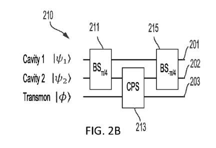
[0070] FIG. 2B illustrates an example quantum circuit diagram 210 for
implementing a
c-SWAP gate using BS operations and CPS operations. First, a first BS
operation 211 with
0 = 7/4 is performed between the first cavity 201 and the second cavity 202.
As described above,
the BS operation may be performed using the coupling transmon 134. After the
first BS
operation 211, a CPS operation 213 between the ancilla transmon 203 and the
second cavity 202
is performed. Finally, a second BS operation 215 with 0 = -7/4 is performed
between the first
cavity 201 and the second cavity 202.
[0071] As shown in Fig. 2C, the c-SWAP gate can be represented in terms
of
conventional linear optical diagram with a first optical mode 231 a second
optical mode 232 and
a transmon 232. The diagram is a Mach-Zehnder interferometer 230 built from a
first beam
splitter 234, a second beam splitter 235, and a controlled phase shifter 236
that implements a 0 or
a it phase shift on one arm controlled by the state of the transmon. For
transmon state Ig), there is
a 0 phase shift and thus no exchange of the two bosonic modes. For transmon
state le), there is a
it phase shift (for each and every excitation coupled with the transmon)
leading to full exchange
(SWAP) between the two optical modes 231 and 232. Hence, in some embodiments,
the c-
SWAP can be used as a special quantum-controlled router, which uses a quantum
state (e.g., the
state of an ancilla transmon) to control the pathway of quantum signals
(carried by the optical
modes).
[0072] In some embodiments, an e-SWAP operation may be performed using a
combination of c-SWAP gates and ancilla transmon rotations. The e-SWAP
operates on two
cavities and is represented by the unitary operator:
UeswAp(0) = exp[i0SWAP] = cost) + isin0 SWAP. (7)
[0073] For 0= 7/2, an e-SWAP gate is equivalent to a SWAP gate, where the
resulting
global phase shift (i) is non-observable. For 0= 7/4, UeswAp(7/4) = 1/V2(/ +
iSWAP) is a
14
CA 03085954 2020-06-15
WO 2019/156759 PCT/US2019/012440
coherent combination of the identity operator and the SWAP operator, and is
sometimes denoted
as VSWAP. Single-qubit rotations and the VSWAP operator operating on qubits
form a set of
universal quantum gates.
[0074] There are similarities and differences between the e-SWAP operator
and the
beam-splitter unitary operator. For the bosonic subspace with zero and one
total excitations, the
two are equivalent (e.g., Uss(0)10,, lb) = cos010,, lb) + isin011,, Ob) =
UeswAp(0)10,, lb)). However,
for the subspace with more than one total excitations, the two operators
behave differently (e.g.,
Uss(0)11,, lb) = cos2011,, lb) + sin20 (12,, Ob) +10,, 2b)), which is distinct
from
A/2
UeswAp(0)11,, lb) =11,, lb)).
[0075] One feature of e-SWAP operator is that it preserves the logical
subspace with
respect to single-mode bosonic encodings that contain arbitrary numbers of
bosons. For logical
states of arbitrary single-mode bosonic encoding Ipi),Ip2) E ,lec, the e-SWAP
operation
UeswAp(0)191),I92)b = cos0 I91),I92)b + isinOlp2),Ipi)b preserves the code
space for any bosonic
codes and for any parameter 0. This important property enables one to carry
out quantum
information processing with different choices of bosonic encoding using the
same hardware.
This powerful feature gives great flexibility to the hardware and allows
experimentation with
different encodings for quantum error correction via 'software updates' on
fixed hardware.
[0076] In some embodiments, the e-SWAP operator between two cavity modes
can be
implemented using a two-level ancilla transmon. For example, FIG. 3A is a
quantum circuit
diagram 300 between a first cavity 301, a second cavity 302 and an ancilla
transmon 303. The
illustrated method for implementing the e-SWAP operation is as follows: (1)
initialize the ancilla
transmon 303 to the quantum statel+ ) = 1W2(1g) + le)); (2) perform a first c-
SWAP operation
311 between the first cavity 301 and the second cavity 302 controlled based on
the state of the
ancilla transmon 303; (3) rotate 312 the ancilla transmon 303 by angle 20
around the X axis
Xe = ei"x; and (4) perform a second c-SWAP operation 313 between the first
cavity 301 and the
second cavity 302 controlled based on the state of the ancilla transmon 303.
After the foregoing
method, the ancilla transmon is restored to the initial statel+ ) and
decoupled from the two
cavity modes; meanwhile, the two cavity modes undergo the e-SWAP operation,
UeswAp(0). If
the ancilla transmon 303 is measured 314, the result, assuming no errors, is
the initial statel+ ).
CA 03085954 2020-06-15
WO 2019/156759 PCT/US2019/012440
[0077] FIG. 3B illustrates a quantum circuit diagram 320 for implementing
the e-SWAP
operation of FIG. 3A using BS operations and CPS operations. In this example,
the c-SWAP
gates are simply replaced with the c-SWAP method shown in FIG. 2B. Thus, the
method of
implementing the e-SWAP gate includes: (1) initializing the ancilla transmon
303 to the quantum
state I +) = 1W2(1g) + le)); (2) performing a first BS operation 321 with 0 =
7r/4 between the
first cavity 301 and the second cavity 302; (3) performing a first CPS
operation 322 between the
second cavity 302 and the ancilla transmon 303; (4) performing a second BS
operation 323 with
o = ¨7r/4 between the first cavity 301 and the second cavity 302; (5)
performing a rotation 324
on the ancilla transmon 303 by angle 20 around the X axis Xe = ei"x; (6)
performing a third BS
operation 325 with 0 = 7r/4 between the first cavity 301 and the second cavity
302; (7)
performing a second CPS operation 326 between the second cavity 302 and the
ancilla transmon
303; (8) performing a fourth BS operation 327 with 0 = ¨7r/4 between the first
cavity 301 and
the second cavity 302. As in FIG. 3A, if the ancilla transmon 303 is measured
328, the result,
assuming no errors, is the initial state I +).
[0078] In some embodiments, a simplified and more robust implementation
of the e-
SWAP operator can be obtained by decomposing the c-SWAP operators into beam
splitter
operators and CPS gates in a way that is different from simply substituting
the quantum circuit
diagram 210 of FIG. 2B into the quantum circuit diagram 300 of FIG. 3A. The
simplification of
the quantum circuit diagram 320 comes from the realization the two of the beam
splitter
operations are redundant (e.g., the second and third beam splitter operations
323 and 325) as they
cancel each other and can therefore be removed. In addition, the transmon can
be initialized in
the ground state and additional Hadamard gates can be added to act on the
transmon just before
the first CPS gate 322 and after the second CPS gate 326, so that the transmon
is kept in the
ground state during the beam splitter unitary operations.
[0079] With the aforementioned two changes to the quantum circuit, a more
robust
quantum circuit diagram 340 for the e-SWAP operation is achieved, as
illustrated in FIG. 3C.
The method of implementing the e-SWAP gate includes: (1) initializing the
ancilla transmon 303
to the quantum state I g); (2) performing a first BS operation 341 with 0 =
7r/4 between the
first cavity 301 and the second cavity 302; (3) performing a first Hadamard
operation 342 on the
ancilla transmon 303; (4) performing a first CPS operation 343 between the
second cavity 302
and the ancilla transmon 303; (5) performing a rotation 344 on the ancilla
transmon 303 by angle
16
CA 03085954 2020-06-15
WO 2019/156759 PCT/US2019/012440
20 around the X axis X0= ei"x; (6) performing a second CPS operation 345
between the second
cavity 302 and the ancilla transmon 303; (7) performing a second Hadamard
operation 346 on
the ancilla transmon 303; (8) performing a second BS operation 347 with 0 =
¨7r/4 between
the first cavity 301 and the second cavity 302. If the ancilla transmon 303 is
measured 348, the
result, assuming no errors, is the initial state I g).
[0080] The simplified quantum circuit diagram 340 include the
aforementioned changes
because the beam splitter operation may be relatively slow compared to the
other operations.
Thus, the quantum circuit in FIG. 3C has both a shorter total time duration
(which reduces the
risk of an error occurring in the cavity states) and a shorter duration for
the period in which the
ancilla transmon is in the excited state (which reduces the risk of an error
occurring on the
ancilla). In the quantum circuit designs of FIG. 3A and 3B, the transmon is
never in the ground
state, making the transmon vulnerable to decoherence throughout the entire
operation, especially
during the relatively slow beam splitter unitary operation. In contrast, the
quantum circuit
diagram 340 of FIG. 3C keeps the transmon in the ground state, except during
the relatively fast
Hadamard, CPS and X0 gates. Therefore, in some embodiments, the quantum
circuit design
efficiently mitigates imperfections due to transmon decoherence, reducing the
error of the overall
quantum gate from O[7 a 1-
t,BS -CPS-FtTrans)] to O[yt(tCPS tTrans)], where yt is the transmon
decoherence rate, tBs, tcps, and t .Ttans are times associated with the beam
splitter, CPS, and
transmon rotation gates (e.g., X0 and H) , respectively. In some embodiments,
tBs( 101us)>>tcps( 1,us)>>tTrans( lOns), and making it advantageous to
eliminate the
vulnerability to transmon decoherence during tBs.
[0081] In some embodiments, the e-SWAP operator can be extended to
operate over
more than two cavities. For example, FIG. 4A illustrates a quantum circuit
diagram 400 where an
e-SWAP is performed using four cavities with UeswAp(a b 'a' b') = exp[i0SWAPa,
b SWAPa', b'].
The four-cavity e-SWAP method 400 includes, after initilizing the ancilla in
the : (1) initializing
the ancilla transmon 403 to the quantum state I +) = 1W2(1g) + le)); (2)
performing a first c-
SWAP operation 411 between the first cavity 401 and the second cavity 402
controlled by the
state of the ancilla transmon 403; (3) performing a second c-SWAP operation
412 between the
third cavity 404 and the fourth cavity 404 controlled by the state of the
ancilla transmon 403; (4)
performing a rotation 415 on the ancilla transmon 403 by angle 20 around the X
axis X0= ei"x;
(5) performing a third c-SWAP operation 413 between the third cavity 404 and
the fourth cavity
17
CA 03085954 2020-06-15
WO 2019/156759 PCT/US2019/012440
404 controlled by the state of the ancilla transmon 403; and (6) performing a
fourth c-SWAP
operation 414 between the first cavity 401 and the second cavity 402
controlled by the state of
the ancilla transmon 403. If the ancilla transmon 403 is measured 415, the
result, assuming no
errors, is the initial state I +).
[0082] Similar to the procedure of FIGS. 3B-C for the e-SWAP between two
modes, the
e-SWAP operation for four modes can be decomposed into beam splitter
operations and CPS
gates (FIG. 4B) and converted to a more robust quantum circuit (FIG. 4C).
Thus, the method of
implementing the e-SWAP gate illustrated by the quantum circuit diagram 420 in
FIG. 4B
includes: (1) initializing the ancilla transmon 303 to the quantum state I +)
= 1W2(Ig) + le)); (2)
performing a first BS operation 421 with 0 = 7r/4 between the first cavity 401
and the second
cavity 402; (3) performing a second BS operation 422 with 0 = 7r/4 between the
third cavity
404 and the fourth cavity 405; (4) performing a first CPS operation 423
between the second
cavity 402 and the ancilla transmon 403; (5) performing a second CPS operation
423 between
the third cavity 404 and the ancilla transmon 403; (6) performing a third BS
operation 425 with
61 = ¨7r/4 between the first cavity 401 and the second cavity 402; (7)
performing a fourth BS
operation 426 with 0 = ¨7r/4 between the third cavity 404 and the fourth
cavity 405; (8)
performing a rotation 427 on the ancilla transmon 403 by angle 20 around the X
axis Xe = ei"x;
(9) performing a fifth BS operation 428 with 0 = 7r/4 between the first cavity
401 and the
second cavity 402; (10) performing a sixth BS operation 429 with 0 = 7r/4
between the third
cavity 404 and the fourth cavity 405; (11) performing a third CPS operation
430 between the
third cavity 404 and the ancilla transmon 403; (12) performing a fourth CPS
operation 431
between the second cavity 402 and the ancilla transmon 403; (13) performing a
seventh BS
operation 432 with 0 = ¨7r/4 between the first cavity 401 and the second
cavity 402; (7)
performing a eighth BS operation 433 with 0 = ¨7r/4 between the third cavity
404 and the
fourth cavity 405. If the ancilla transmon 403 is measured 415, the result,
assuming no errors, is
the initial state I +).
[0083] It should be noted that not all operations have to be performed in
the order
shown. For example, the first BS operation 421 and the second BS operation 422
are
illustrated to be performed at the same time. In some embodiments, either BS
operation
may be performed before the other. The same is true for the third BS operation
425 and the
fourth BS operation 426; the fifth BS operation 428 and the sixth BS operation
429; and the
18
CA 03085954 2020-06-15
WO 2019/156759 PCT/US2019/012440
seventh BS operation 432 and the eighth BS operation 433. Also, the first CPS
operation
423 is illustrated as occurring before the second CPS operation 424. In some
embodiments,
the second CPS operation 424 may be performed before the first CPS operation
423.
Similarly, the fourth CPS operation 431 may be performed before the third CPS
operation
430.
[0084] Following the example of simplifying the quantum circuit diagram
of FIG. 3C
and making the method more robust to errors, the quantum circuit diagram 450
of FIG. 4C
includes: (1) initializing the ancilla transmon 303 to the quantum state I g);
(2) performing a first
BS operation 451 with 0 = 7r/4 between the first cavity 401 and the second
cavity 402; (3)
performing a second BS operation 452 with 0 = 7r/4 between the third cavity
404 and the
fourth cavity 405; (4) performing a first Hadamard operation 453 on the
ancilla transmon 403;
(5) performing a first CPS operation 454 between the second cavity 402 and the
ancilla transmon
403; (6) performing a second CPS operation 455 between the third cavity 404
and the ancilla
transmon 403; (7) performing a rotation 456 on the ancilla transmon 403 by
angle 20 around the
X axis Xe = ei"x; (8) performing a third CPS operation 457 between the third
cavity 404 and the
ancilla transmon 403; (9) performing a fourth CPS operation 458 between the
second cavity 402
and the ancilla transmon 403; (10) performing a second Hadamard operation 459
on the ancilla
transmon 403; (11) performing a third BS operation 460 with 0 = ¨7r/4 between
the first cavity
401 and the second cavity 402; (12) performing a fourth BS operation 461 with
0 = ¨7r/4
between the third cavity 404 and the fourth cavity 405. If the ancilla
transmon 403 is measured
415, the result, assuming no errors, is the initial state I g).
[0085] It should be noted that not all operations have to be performed in
the order
shown. For example, the first BS operation 451 and the second BS operation 452
are
illustrated to be performed at the same time. In some embodiments, either BS
operation
may be performed before the other. The same is true for the third BS operation
460 and the
fourth BS operation 461. Also, the first CPS operation 454 is illustrated as
occurring before
the second CPS operation 455. In some embodiments, the second CPS operation
455 may
be performed before the first CPS operation 454. Similarly, the fourth CPS
operation 458
may be performed before the third CPS operation 457.
19
CA 03085954 2020-06-15
WO 2019/156759 PCT/US2019/012440
[0086] Returning now to the quantum circuit diagram 340 of FIG. 3C, the
presence of
dephasing and decay errors are discussed. Since tcps'>>t õ .Trans, the focus
is on transmon errors
during the two CPS gates, while neglecting the errors during Xe
[0087] In some embodiments, the quantum circuit diagram 340 for the e-
SWAP
operation illustrated in FIG. 3C can herald transmon dephasing errors, which
occur with a
dephasing rate y. The transmon dephasing error in the g-e subspace can be
characterized by the
quantum channel
6'(p) = (1 - (Op + ccrzpaz, (8)
where c = -21 (1 - e-Y(PtcPs) for transmon dephasing error probability during
each CPS gate and
o-z= Ig)(gl- le)(el for 7 relative phase jump between the Ig) and le) states.
Transmon dephasing
during either of the two CPS gates results in a measured le) state for the
transmon at the
measurement 348, which is orthogonal to Ig) and can be detected without
ambiguity. Hence, in
some embodiments, any first-order (i.e. single-occurrence) transmon dephasing
errors during the
CPS gates are detected, though as noted above, which of the two errors
occurred cannot be
determined and, therefore, the errors are only heralded and cannot be
corrected.
[0088] In some embodiments, additional levels of the ancilla transmon,
beyond the
ground state g) and the first excited state le), may be used to improve the
robustness of the e-
SWAP operation. For example, first-order errors associated with spontaneous
decay of the
transmon state may be both heralded and corrected. In some embodiments, the
cavity-transmon
coupling Hamiltonian is altered to be "error transparent", so that the leading
order error of
transmon decay commutes with the error transparent Hamiltonian for all logical
states of the
cavities. The transmon decay that occurred during the evolution can then be
identified as the
transmon decay that occurred at the end of the evolution, which can
significantly simplify the
error analysis.
[0089] In some embodiments, four transmon levels (Ig), Ir), Ir'), le))
are used, where the
Ig)-le) subspace is used to encode a qubit of information, while the Ir)-Ir'),
lsubspace is used to
detect errors. FIG. 5A illustrates an energy level diagram 500 for the
transmon. The state le) 501
represents some higher excited level (e.g., higher than the first excited
state), that does not
directly decay to state Ig) 502, but decays to state Ir) 503 as a leading
decay error. By introducing
additional levels, the transmon decay error from the Ig)-le) subspace can be
characterized by the
quantum channel
CA 03085954 2020-06-15
WO 2019/156759 PCT/US2019/012440
E(P) =
KiPKi (9)
J=0,1,===
where Ko = Ig)(g1+ V1 - e-Yitcpsle)(el and Ki = e¨Yitcps/2 Ir)(el. The
subspace spanned by Ig)-
le) is used to encode the qubit, whereas the subspace spanned by le), Ir), and
le) has uniform
strength of dispersive coupling with the cavity mode.
[0090] In some embodiments, a quantum circuit similar to the circuit
shown in FIG. 3C is
used, but the unitary operations are generalized to the four-level transmon.
In some
embodiments, controllable back-action to the cavity modes is controlled by
engineering the
dispersive coupling between the transmon and cavity
Ha's = hx(le)(el + Ir)(r1+ Ir')(r'1)01i, (10)
to have identical dispersive shift x for states le), Ir), and Ir'), so that
the CPS gate is
CPS = Ig)(g10/+ (1e)(el + Ir)(r1+ 10(r'1)0( ¨ 1)11. (11)
[0091] In some embodiments, the unitary operator associated with a
generalized
Hadamard gate becomes
H Ig) = (10+10012
H le) = (10-10012 (12)
H Ir) = Ir)
H Ir') = Ir').
[0092] Thus, the Hadamard rotation is performed within the g-e subspace
and acts
trivially over the r-r' subspace.
[0093] In some embodiments, the transmon rotation becomes
Xe Ig) = cosOlg) + isinOle)
Xe le) = isinOlg) + cosOle) (13)
Xe Ir) = Ir')
Xe Ir') =10,
which rotates within the g-e subspace and swaps states Ir) and Ir').
[0094] In some embodiments, the CPS operation becomes
CPS I g) = Ig)0(+1)11.
CPS le) = le)0(-1)1 (14)
CPS Ir) = 1r)0(-1)11
CPS 10 = 100(-
21
CA 03085954 2020-06-15
WO 2019/156759 PCT/US2019/012440
[0095] With the above extended gates over the four-level transmon, it is
possible to
detect first-order transmon dephasing errors and correct first-order transmon
decay errors.
[0096] Transmon decay during the first CPS operation 343 results in
measurement 348 of
Ir') for the transmon state, while the cavity modes continue to evolve under
the CPS gate without
error because the decay does not change the dispersive coupling. Transmon
decay during the
second CPS operation 345 results in measurement of Ir) for the transmon state,
while the cavity
modes evolve as the desired UeswAp(0). Because the transmon decay errors (1e)
and Ir) states
associated with transmon decay during the first and second CPS gates,
respectively) can be
unambiguously distinguished, the first-order transmon decay errors during the
CPS gates can be
actively corrected in some embodiments.
[0097] In some embodiments, three transmon levels (Ig), Ir), le)) may be
used by
collapsing the r-r' subspace to a single state Ir) and reducing the operations
within the r-r'
manifold to trivial operation on state Ir) (e.g., X0 Ir) = Ir)). In some
embodiments, such a detection
scheme can also detect transmon thermal heating (e.g., Ig) ¨> Ir)). A three-
level transmon ancilla
mode is therefore sufficient to achieve detection of first-order transmon
dephasing/decay/heating
errors during the CPS gates.
[0098] In some embodiments, both decay and heating errors of the transmon
are
corrected by deploying additional transmon levels. For example, six transmon
levels 511-516
(Ig), le), Ir), Ir'), Is), Is')) with decay transitions shown in the energy
level diagram 510 of FIG. 5B
and dispersive coupling in Eqn. (10) can be used. In some embodiments, a qubit
of information
is encoded in the g-e subspace. Based on a measurement of the transmon state
resulting in le) or
Ir, ) a transmon decay error during the first or second CPS gates can be
corrected. Based on a
measurement of the transmon state of Is') or Is), a transmon heating error
during the first or
second CPS gates can be corrected.
[0099] Some embodiments use the above-discussed techniques in a variety
of
applications. Such as a quantum router, quantum RAM, quantum state comparison,
quantum
principal component analysis, or universal quantum computing.
[0100] In a modular architecture for information processing, routers play
an
indispensable role in connecting different modules and different components
within a module.
There are many different types of routers for classical and quantum
information processing. As
listed in Table 1, routers may be classified based on the classical/quantum
(C/Q) nature of the
22
CA 03085954 2020-06-15
WO 2019/156759 PCT/US2019/012440
input signals and control signals. Different types of routers and example
associated applications.
A classical-classical router is simply a classical switch. A classical-quantum
router sends
quantum information to a classical address. A quantum-quantum router sends
quantum
information to a quantum superposition of addresses. The quantum-classical
router sends
classical information to a quantum address. However since the information is
classical the
quantum state collapses so that only one address receives the classical
signal. This is what
happens in a quantum measurement where a semi-classical 'meter' is entangled
with a quantum
state and the state 'collapses' when the meter is 'read'
Control\Input Classical Quantum
Classical C-C Router C-Q Router
(e.g., classical switch) (e.g., quantum network)
Quantum Q-C Router Q-Q Router
(e.g., quantum measurement) (e.g., quantum RAM)
Table 1
[0101] In some embodiments, a Q-Q router is implemented using the c-SWAP
operation
by: (1) storing quantum input and control signals in the cavity and transmon
modes, respectively,
(2) applying the c-SWAP operation over the cavity modes conditioned on the
transmon modes,
and (3) retrieving the quantum signals from the cavity and transmon modes.
[0102] In some embodiments, the c-SWAP operation can be used to implement
a
quantum Random Access Memory (RAM). The quantum RAM can perform memory
accesses
using a coherent quantum superposition of addresses. To build an efficient
quantum RAM, a Q-
Q router with a three-level (transmon) memory (labeled "0", "L", and "R") and
three cavity
modes (labeled "input", "left", and "right") is used. The (transmon) memory is
initialized in the
"0" state, and all three cavities are initialized in the vacuum Ivac) state.
The goal of the Q-Q
router is to process or route the quantum signal(s), which can be a
superposition of three possible
states: vacuum Ivac), left IL), or right IR).
[0103] In some embodiments, a Q-Q router has five different function
settings: (1) idle,
(2) store control signal, (3) route signal forward, (4) route signal backward,
and (5) retrieve
23
CA 03085954 2020-06-15
WO 2019/156759 PCT/US2019/012440
control signal. Note that steps (2) & (3) can be used to carve out the pathway
towards the target
memory, while steps (4) and (5) can be used for the inverse unitary to
decouple the quantum
RAM.
[0104] In some embodiments, the operation of each of these five function
settings is as
follows:
(1) When the Q-Q router idles, no operation need to be applied.
(2) To store a control signal, the Q-Q router stores the incoming control
signal in
the input cavity, and then transfers the control signal from the input cavity
to the transmon
mode.
(3) To route the signal forward, the Q-Q router stores the signal in the input
cavity
temporarily. Then, conditioned on the (transmon) memory being in the state
"0", "L", or "R",
the Q-Q router guides the quantum signal (via c-SWAP operations) to the
"input", "left", or
"right" cavity, respectively. Finally, the Q-Q router releases the signal from
the "left" and
"right" cavities to allow it to move on to the next stage.
(4) To route the signal backward, the Q-Q router performs the reverse
operation
of (3). For example, the Q-Q router stores the incoming signal to the "left"
and "right"
cavities. Then, conditioned on the (transmon) memory states "0", "L", or "R",
the Q-Q router
guides the quantum signal (via c-SWAP operations) from the "input", "left", or
"right" cavity
to the "input" cavity, respectively. Finally, the Q-Q router retrieves the
signal from the input
cavity.
(5) To receive the control signal, the Q-Q router performs the reverse
operation of
(2). For example, the Q-Q router transfers the control signal from the
(transmon) memory to
the input cavity, and then retrieves the signal from the input cavity.
[0105] In some embodiments, the c-SWAP operation can be used to estimate
the overlap
of two quantum states. For example, if the transmon is initialized in the
state Ig) + le) and the
quantum state for two subsystems (cavities) are represented by the density
matrices pA and pB,
the initial input state is:
(Ig) + le))((g1+ (e1)0pA0pB . (15)
[0106] After the c-SWAP operation, the state becomes:
Ig)(g1 OpA0pB + !Mel [(A OpB)SWAPAB] +
le)(g1 0[SWAPAB(pA (V)] + le)(el 0[SWAPAB(pA OpB)SWAPAB], (16)
24
CA 03085954 2020-06-15
WO 2019/156759 PCT/US2019/012440
with reduced density matrix taking the form
ptransmon = 1g)(g1+ Ig)(elTrpApB + le)(gITrpApB + le)(el (17)
where we have used the property
Tr[(pA0pB)SWAPAB] = TrRpi, jA Opk, /BA,
= 11,1 P1,1A P1,13 (18)
TrpA pB
TrpB pA
[0107] Thus, in some embodiments, by measuring the phase coherence (e.g.,
Ramsey
fringe contrast) of ptransmon, the overlap 0(pA , pB) TrpApB , which is always
a real number, can be
extracted.
[0108] In some embodiments, the transmon is projectively measured in the
Ig) 1e) basis.
If the transmon is measured as Ig) + le), the two subsystems are projected to
the symmetric
subspace (i.e., the eigen-subspace with eigenvalue + 1 for the SWAP operator),
(19)
where + is a projection operator. If the transmon is measured in Ig) ¨ le),
the two subsystems
are projected to the anti-symmetric subspace (i.e., the eigen-subspace with
eigenvalue ¨ 1 for the
SWAP operator),
(20)
where projection operator H _ = 1 ¨11+. A subsequent measurement should give
the same
outcome, which is consist with the quantum non-demolition nature of these
measurements.
[0109] In some embodiments, a more robust quantum circuit 600 acting on a
first cavity
601, a second cavity 602, and a transmon 603, as illustrated in FIG. 6, for
the purpose of
quantum state comparison includes the following modifications: (1) remove the
second beam-
splitter (See FIG. 2B) that is dispensable for the purpose of quantum state
comparison; (2)
initialize the transmon in Ig) and rotate to Ig) + le) right before the CPS
gate to avoid the
transmon decoherence during the first beam-splitter operation. The simplified
circuit 600
minimizes the use of the beam splitter operation and decoherence of the
transmon probe and
includes: (1) a first beam splitter operation 605 between the first cavity 601
and the second
cavity 602; (2) a first Hadamard operation 606 on the transmon 603; (3) a CPS
operation 607
between the second cavity 602 and the transmon 603; (4) a second Hadamard
operation 608 on
the transmon 603; and (5) a measurement 609 of the transmon 603 state. Note
that the simplified
CA 03085954 2020-06-15
WO 2019/156759 PCT/US2019/012440
circuit can also be interpreted as the parity measurement of the second cavity
mode after the
beam-splitter operation. This interpretation can be easily justified based on
the property of the
projection operator to the symmetric subspace II + , which is spanned by the
symmetric states
(at _ bt)2( n,at
+ bt)mlvac) with non-negative integers n, m (similarly, the anti-symmetric
subspace
n + l(
at _ is spanned by the anti-symmetric states (at _ bt)2 1(at + btrIvac).
Recall that after the
50/50 beam splitter, at bt correspond to the creation operators of the first
and second cavity
modes, respectively. Therefore, the symmetric states always have 2n even
excitations in the
second cavity mode, while the antisymmetric states always have 2n + 1 odd
excitations.
[0110] For each of pA and pB, a binary outcome 0 or 1 associated with the
transmon
measurement is obtained. N ¨ c- 2 pairs of pA and pB are needed to reliably
estimate the overlap
0p'1, pB) with precision c.
[0111] In some embodiments, an e-SWAP operation is used to perform
quantum
principal component analysis (qPCA), which may be used to perform machine
learning from
large data sets. More specifically, qPCA can reveal the largest eigenvalues of
an ensemble of
identically prepared density matrices. The key idea is to use the following
property of e-SWAP
iswApAvekT)eiswApAt = er _ z e- IpAto_eipAt
Trpe- iAt[p,(31+ 0(At2) ,
(21)
which effectively simulates the Hamiltonian evolution with Hamiltonian being
the Hermitian
density matrix H = p for small duration At. With n identical copies of the
density matrix p, one
can construct e- tpnAto_etpnAt . In some embodiments, together with a quantum
phase estimation
algorithm, the phase associated with the largest few eigenvalues of the
density matrix p can be
efficiently estimated. The e-SWAP gate according to some embodiments herein
will enable the
physical implementation for the key step of the qPCA.
[0112] In some embodiments, the e-SWAP gate is used to achieve universal
quantum
computing with bosonic systems, which can be compatible with arbitrary single-
mode bosonic
encoding (denoted as 15) and li)). For example, if one encodes one logical
qubit using four such
bosonic modes, with quad-rail logical qubit basis as
100 = 1/2 (15i) + 11O))1,20(161) ¨ lid))3,4 (22)
11Q) = 1/2 (15i) ¨ 11O))1,20(151) +1i5))3,4,
where the sub-indices label the modes. Sincel5T) 1i5) are respectively
eigenstates of the SWAP
operator with eigenvalues 1, the quad-rail logical Z-rotation is the e-SWAP
operation
4(0) = exp[ ¨ i0SWAP1,2] = exp [i0SWAP3, 4] . (23)
26
CA 03085954 2020-06-15
WO 2019/156759 PCT/US2019/012440
[0113] In addition, we have SWAP1, 3 SWAP2, 410Q) = 11Q) = XQI0Q), which
implies that
the quad-rail logical X-rotation is a four-mode e-SWAP operation
XQ(0) = exp[ ¨ i0SWAP1,3 SWAP2, 4] . (24)
[0114] Finally, the controlled-Z gate between the two encoding quad-rail
logical qubits is
another four-mode e-SWAP operation
CZ(0) = exp[ ¨ i0SWAPi, 2 SWAP r , 2'], (25)
where the sub-indices l' and 2' label the first two bosonic modes from the
other quad-rail logical
qubit. Given an arbitrary logical Z- and X-rotations and controlled-Z gate, it
is sufficient to
achieve arbitrary universal quantum computation. Because the above gates do
not depend on the
details of the choice of orthogonal basis 15) and Li), this scheme can work
for any single-mode
bosonic encoding, including a cat code, a binomial code, a GKP code, etc.
Therefore, the
aforementioned robust design of e-SWAP implementations (see FIG. 4C) is
sufficient to
implement the key ingredients for universal quantum computation.
[0115] Having thus described several aspects and embodiments of the
technology set
forth in the disclosure, it is to be appreciated that various alterations,
modifications, and
improvements will readily occur to those skilled in the art. Such alterations,
modifications, and
improvements are intended to be within the spirit and scope of the technology
described herein.
For example, those of ordinary skill in the art will readily envision a
variety of other means
and/or structures for performing the function and/or obtaining the results
and/or one or more of
the advantages described herein, and each of such variations and/or
modifications is deemed to
be within the scope of the embodiments described herein. Those skilled in the
art will recognize,
or be able to ascertain using no more than routine experimentation, many
equivalents to the
specific embodiments described herein. It is, therefore, to be understood that
the foregoing
embodiments are presented by way of example only and that, within the scope of
the appended
claims and equivalents thereto, inventive embodiments may be practiced
otherwise than as
specifically described. In addition, any combination of two or more features,
systems, articles,
materials, kits, and/or methods described herein, if such features, systems,
articles, materials,
kits, and/or methods are not mutually inconsistent, is included within the
scope of the present
disclosure.
[0116] Also, as described, some aspects may be embodied as one or more
methods. The
acts performed as part of the method may be ordered in any suitable way.
Accordingly,
27
CA 03085954 2020-06-15
WO 2019/156759 PCT/US2019/012440
embodiments may be constructed in which acts are performed in an order
different than
illustrated, which may include performing some acts simultaneously, even
though shown as
sequential acts in illustrative embodiments.
[0117] All definitions, as defined and used herein, should be understood
to control over
dictionary definitions, definitions in documents incorporated by reference,
and/or ordinary
meanings of the defined terms.
[0118] The indefinite articles "a" and "an," as used herein in the
specification and in the
claims, unless clearly indicated to the contrary, should be understood to mean
"at least one."
[0119] The phrase "and/or," as used herein in the specification and in
the claims, should
be understood to mean "either or both" of the elements so conjoined, i.e.,
elements that are
conjunctively present in some cases and disjunctively present in other cases.
Multiple elements
listed with "and/or" should be construed in the same fashion, i.e., "one or
more" of the elements
so conjoined. Other elements may optionally be present other than the elements
specifically
identified by the "and/or" clause, whether related or unrelated to those
elements specifically
identified. Thus, as a non-limiting example, a reference to "A and/or B", when
used in
conjunction with open-ended language such as "comprising" can refer, in one
embodiment, to A
only (optionally including elements other than B); in another embodiment, to B
only (optionally
including elements other than A); in yet another embodiment, to both A and B
(optionally
including other elements); etc.
[0120] As used herein in the specification and in the claims, the phrase
"at least one," in
reference to a list of one or more elements, should be understood to mean at
least one element
selected from any one or more of the elements in the list of elements, but not
necessarily
including at least one of each and every element specifically listed within
the list of elements and
not excluding any combinations of elements in the list of elements. This
definition also allows
that elements may optionally be present other than the elements specifically
identified within the
list of elements to which the phrase "at least one" refers, whether related or
unrelated to those
elements specifically identified. Thus, as a non-limiting example, "at least
one of A and B" (or,
equivalently, "at least one of A or B," or, equivalently "at least one of A
and/or B") can refer, in
one embodiment, to at least one, optionally including more than one, A, with
no B present (and
optionally including elements other than B); in another embodiment, to at
least one, optionally
including more than one, B, with no A present (and optionally including
elements other than A);
28
CA 03085954 2020-06-15
WO 2019/156759 PCT/US2019/012440
in yet another embodiment, to at least one, optionally including more than
one, A, and at least
one, optionally including more than one, B (and optionally including other
elements); etc.
[0121] Also, the phraseology and terminology used herein is for the
purpose of
description and should not be regarded as limiting. The use of "including,"
"comprising," or
"having," "containing," "involving," and variations thereof herein, is meant
to encompass the
items listed thereafter and equivalents thereof as well as additional items.
[0122] In the claims, as well as in the specification above, all
transitional phrases such as
"comprising," "including," "carrying," "having," "containing," "involving,"
"holding,"
"composed of," and the like are to be understood to be open-ended, i.e., to
mean including but
not limited to. Only the transitional phrases "consisting of' and "consisting
essentially of' shall
be closed or semi-closed transitional phrases, respectively.
29