Note: Descriptions are shown in the official language in which they were submitted.
CA 03087275 2020-06-25
WO 2019/143876 PCT/US2019/014108
MEMS DEVICE FOR AN IMPLANT ASSEMBLY
CROSS-REFERENCE TO RELATED APPLICATIONS
[0001] This application claims priority to and the benefit of each the
following
applications: U.S. Provisional Patent Application No. 62/618,848 entitled
"MEMS
DEVICE FOR AN IMPLANT ASSEMBLY," filed on January 18, 2018. This
application is also a continuation-in-part of U.S. Patent Application No.
15/213,712
entitled "PRESSURE SENSING IMPLANT" filed on July 19, 2016 which is a
continuation-in-part of U.S. Patent Application No. 14/777,654 entitled
"PRESSURE
SENSING IMPLANT" filed on September 16, 2015 which is a national phase entry
application that claims priority to International Patent Application No.
PCT/U52014/030661 filed March 17, 2014 which claims priority to Provisional
Patent Application No. 61/786,793 entitled "PRESSURE SENSING IMPLANT,"
filed on March 15, 2013. U.S. Patent Application No. 15/837,075 entitled
"IMPLANTABLE SENSOR ENCLOSURE WITH THIN SIDEWALLS," filed on
December 11, 2017, which claims priority to U.S. Patent Application No.
14/129,725
(U.S. Patent No. 9,867,552) entitled "IMPLANTABLE SENSOR ENCLOSURE
WITH THIN SIDEWALLS," filed on February 21, 2014, which claims priority to
International Patent Application No. .. P CT/US/2012/044998 ..
entitled
"IMPLANTABLE SENSOR ENCLOSURE WITH THIN SIDEWALLS," filed on
CA 03087275 2020-06-25
WO 2019/143876
PCT/US2019/014108
June 29, 2012 which claims priority to Provisional Patent Application No.
61/502,982
entitled "IMPLANTABLE SENSOR ENCLOSURE WITH THIN SIDEWALLS,"
filed on June 30, 2011, each of which are hereby incorporated by reference in
its
entireties.
FIELD OF INVENTION
[0002] This application relates to implanted sensor packages and more
particularly to
an improved structure for implanted sensor packages.
BACKGROUND
[0003] Implantable wireless sensors are useful in assisting diagnosis and
treatment of
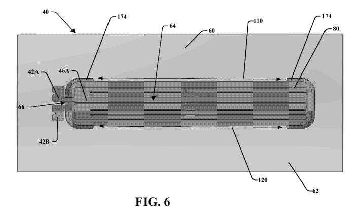
many diseases. Examples of wireless sensor readers are disclosed in U.S.
Patent No.
8,154,389, and US Patent No. 8,493,187, each entitled Wireless Sensor Reader,
which
are incorporated by reference herein. In particular, there are many
applications where
measuring pressure from within a blood vessel deep in a patient's body is
clinically
beneficial. For example, measuring the pressure in the heart's pulmonary
artery is
helpful in optimizing treatment of heart failure and pulmonary hypertension.
In this
type of application, a sensor may need to be implanted up to 20 cm beneath the
surface of the skin.
[0004] One type of implant for this application is described by US Patent
Application
15/213,712 ("the '712 application") which illustrates the use of floating
bases and
vented cavities within a hermetically sealed implant housing. Notably, these
types of
implants include micro-electromechanical systems (MEMS) having capacitive
electrodes that transduce pressure to capacitance. The implants include a
capacitive
sensor that includes a flexible diaphragm and a less flexible (more rigid)
base, with a
cavity in between and capacitive electrodes at least partially extending
within the
2
CA 03087275 2020-06-25
WO 2019/143876
PCT/US2019/014108
cavity. The sensor may be fabricated having a diaphragm formed on one wafer
and a
base formed on a second wafer, in which the base is attached to the diaphragm
around
a perimeter. Two layers ¨ diaphragm and base - thus form a capacitive sensor
in
which the base has a smaller overall area than the diaphragm. The sensor may
then be
attached to an implant housing by inserting the smaller-area base into a
larger housing
cavity of the implant housing and is hermetically sealed therein leaving an
outer
surface of the diaphragm exposed to the environment outside of the implant
housing.
The attachment line between the base and diaphragm within the implant housing
may
be referred to as a "bond line" and the cavity defined between the diaphragm
and base
may be identified as a "capacitive gap." The '712 application discusses
various
embodiments of these devices.
[0005] Known processes for bonding the two wafers together, forming the
capacitive
gap, generally cause various internal stresses at the bond line (i.e. point of
bonding
about the perimeter between the base and diaphragm). As such, a high-stress
line may
be formed around the perimeter of the cavity. The stress may relax over time
slowly,
and/or change with temperature. The stress may case the implant to sense or to
generate inaccurate readings in capacitance over the life of the device as
capacitance
is changing in response to a parameter (e.g. stress or temperature) other than
the
desired measurement (e.g. pressure). Stress relaxation along the bond line may
be a
slow change over time which can cause signal drift due to slow change in
capacitive
gap height.
[0006] It has been identified that the physical features of the capacitive gap
may be
important to the functional performance of the pressure sensing implant. The
capacitance, and hence the resonant frequency of the implant, depends on the
change
3
CA 03087275 2020-06-25
WO 2019/143876
PCT/US2019/014108
in distance between the capacitive electrodes. Thus, it is desirable to have
an implant
whose capacitance changes when the distance between the capacitive electrode
(the
gap height) changes, due to an external pressure. However, it is not desirable
to also
experience capacitance changes due to any other reason, including: slow
changes in
the composition of gas (or fluid) in the capacitive gap over time; slow
changes in
distance between plates due to relaxation of built-in internal stresses over
time; and
changes in temperature. These composition changes may cause error in implant
readings because capacitance (and hence resonant frequency) may be changing
for
reasons other than due to external pressure. In one embodiment, the design of
the
implant is subject to a heightened level of sensitivity as a gap change of 1
percent (i.e.
nanometers) over time may be significant enough to put the implant out of its
designed range or specified functionality.
[0007] Additionally, for implants with vented cavities as discussed above,
there is a
need for the composition of the gap fluid (i.e. liquid or gas) to stabilize
quickly once
the diaphragm and base wafer are hermetically sealed to the cavity of the
implant
housing. If, for example, a component within the implant housing (such as a
PCB)
outgasses water vapor into the housing cavity, and the vent between the
housing
cavity and capacitive gap is only a small hole, it may take a long time for
the
capacitive gap to achieve homogeneity with the outer housing cavity, causing
long
term inaccuracy while the stabilization (homogeneity) takes place.
[0008] Further challenges have been identified related to the practical
implementation
of such an implant. Particularly, it has been identified that an implant
designed to
meet the criteria above may also be sensitive to temperature and pressure
changes,
including while in ambient conditions, when positioned within a patient, and
during
4
CA 03087275 2020-06-25
WO 2019/143876
PCT/US2019/014108
transition between ambient conditions to in vivo. These temperature and
pressure
variations may cause the sensor to communicate inconsistent signals or
otherwise
function in an inconsistent manner. As such, in addition to providing an
implant that
includes desirable features including having high sensitivity, good electrical
isolation
between electrical nodes and surrounding body fluids or tissue, being highly
stable
over time, having good mechanical strength, incorporating biocompatible
materials,
minimizing the use of ferritic materials; the implant may also include a
design that
would increase mechanical strength and reduce the effects of changes to
temperature
and pressure stresses.
[0009] Thus, it is desirable to provide an improved implant to optimize
desirable
features and to ensure a consistent and reliable operation over the life of
the implant.
Further, because MEMS fabrication processes can be complex and require very
long
development times, it is desirable to identify designs that allow modifying
performance specifications with only minor changes in structure. Such
specifications
for an implant include: sensitivity, full scale range, frequency offset, and
avoidance of
pull-in between capacitive electrodes. As such, there is a need for a
capacitive MEMS
pressure sensor with floating base and vented cavity that provides: reduced
gap height
error due to relaxation of internal stresses at the bond line; reduced gap
height error
due to changes in stress at the bond line, due to temperature changes; reduced
capacitance error due to slow, long-term change of composition in the fluid
(gas or
liquid) in the gap; and to provide a cost-effective means to simply modify and
control
key design parameters such as sensitivity, full-scale range, maximum voltage
withstand (pull-in resistance), and temperature sensitivity.
SUMMARY OF THE INVENTION
CA 03087275 2020-06-25
WO 2019/143876
PCT/US2019/014108
[0010] This application relates to hermetically packaged wireless electronics
and
more particularly to an implantable sensor design and manufacturing approach
to
optimize manufacturability, size, longevity, RF characteristics, and overall
performance while minimizing potential effects of operating in various
pressure
conditions, temperature conditions and manufacturing induced stress
conditions.
[0011] In an embodiment, an implant comprises a housing that defines a housing
cavity that includes a sensor connected to said housing. Said sensor comprises
a
diaphragm configured to flex in response to external changes in pressure and a
floating base attached to said diaphragm to define a capacitive gap between
said
diaphragm and said floating base. Said attachment is positioned along a
perimeter of
said capacitive gap wherein said floating base is positioned entirely within
said cavity
and wherein said attachment along said perimeter contains at least one
discontinuity.
The floating base may be attached only to said diaphragm. The sensor may be a
capacitive pressure sensor. The diaphragm may be connected to said housing to
form
a hermetic seal about said housing cavity. The sensor may include at least one
electrical contact positioned on said diaphragm. The at least one
discontinuity may
vent said capacitive gap to said housing cavity such that liquid or gas may
pass
between said gap and said housing cavity.
[0012] The at least one discontinuity may allow at least one electrical trace
to connect
at least one said electrical contact outside of said capacitive gap to at
least one
electrode positioned at least partially within said capacitive gap. The
capacitive gap
may include electrodes positioned on said diaphragm and said floating base.
The
implant may include a coil in electrical communication with said sensor, said
coil
positioned within said housing. The diaphragm may be made of a glass material
and
6
CA 03087275 2020-06-25
WO 2019/143876
PCT/US2019/014108
the floating base may be made of silicon. The diaphragm may include a
thickness of
about 195[tm and said at least one discontinuity may include a length of about
6.75
mm. The location and size of said at least one discontinuity may be configured
to
enhance at least one performance parameter of said implant. The at least one
performance parameter may be selected from the following list: sensitivity to
pressure, sensitivity to temperature, mechanical strength, and long term
accuracy.
Sensitivity to temperature may be improved by positioning said at least one
discontinuity such that a coefficient of thermal expansion mismatch effect
counteracts
a gas expansion effect to reduce capacitive gap change due to temperature.
[0013] In another embodiment, provided is a method of assembling an implant
The
method comprises providing a housing that defines a cavity. A floating base
may be
attached to a diaphragm to form a capacitive gap, said attachment being
positioned
along a perimeter of said capacitive gap and including at least one
discontinuity to
enhance at least one performance parameter of said implant. The diaphragm may
be
attached to said housing such that said floating base is positioned within
said cavity. A
coil may be attached to said sensor. A bottom may be attached to said housing
to form
a hermetic seal about said cavity. The diaphragm may be hermetically attached
to said
housing by at least one laser weld about the perimeter of said cavity. The
diaphragm
may be made of a glass material and said floating base may be made of silicon.
[0014] In another embodiment, provided is an implant that comprises a housing
that
defines a cavity and having a sensor connected to said housing. The sensor
comprising a diaphragm may have at least one diaphragm electrode. A base may
be
attached to said diaphragm, said base including at least one base electrode
wherein
said base and diaphragm define a capacitive gap between the at least one
diaphragm
7
CA 03087275 2020-06-25
WO 2019/143876
PCT/US2019/014108
electrode and the at least one base electrode. The base may attach to said
diaphragm
along a perimeter of said capacitive gap, said attachment including at least
one
discontinuity configured to enhance at least one performance parameter of said
implant. The base may be positioned within the cavity of said housing. The
base may
further include at least one through hole to provide access to electrically
connect said
at least one electrode to a component outside said capacitive gap. The
diaphragm may
include a thickness between about 100[tm to about 300[tm. The implant may
include a
circuit having a resonant frequency that changes in response to a sensed
parameter
such as pressure. The implant may be filled with a liquid or gel or may be a
vacuum
or filed with a predetermined pressure. The base may include at least one
through
substrate via (TSV) to electrically connect the at least one of the base
electrode and
said diaphragm electrode to a component outside said capacitive gap. The
diaphragm
may include a thick region and a thin region wherein said thin region is
aligned with
said capacitive gap. The at least one performance parameter may be selected
from the
following list: sensitivity to pressure, sensitivity to temperature,
mechanical strength,
and long term accuracy. The sensitivity to temperature may be achieved by
positioning said at least one discontinuity such that a coefficient of thermal
expansion
mismatch effect counteracts a gas expansion effect to reduce capacitive gap
change
due to temperature.
[0015] In yet another embodiment, provided is an implant that comprises a
housing
having a plurality of walls and at least one opening. A sensor may be
connected to an
opening in said housing, said sensor comprising a first layer having a first
dimension
and a second layer having a second dimension shorter than said first
dimension. Said
second layer may be positioned entirely within said housing and a surface of
said first
layer is exposed to the exterior of said housing. Said second layer may be
attached to
8
CA 03087275 2020-06-25
WO 2019/143876
PCT/US2019/014108
said first layer to define a capacitive gap between layers, said attachment
being
positioned along a perimeter of said capacitive gap. Said attachment along
said
perimeter may include at least one discontinuity. The location and position of
said at
least one discontinuity may be configured to enhance at least one performance
parameter of said implant.
[0016]
BRIEF DESCRIPTION OF THE DRAWINGS
[0017] Embodiments of the present disclosure are described herein with
reference to
the drawings wherein:
[0018] Figure 1 is a perspective view of an embodiment for a wireless implant
of the
present disclosure;
[0019] Figure 2 is a schematic cross sectional view of a sensor component of
the
wireless implant of the present disclosure;
[0020] Figure 3 is a schematic cross-sectional view of the implant of Figure
1;
[0021] Figure 4 is a bottom schematic view of a portion of a partially
assembled
implant with a printed circuit board for an embodiment of the implant;
[0022] Figure 5A is a top schematic view of a known sensor component of the
implant separate from an implant housing;
[0023] Figure 5B is a top perspective schematic view of the known sensor
component
of the instant separate from the implant housing;
[0024] Figure 6 is a top schematic view of a sensor component of the instant
disclosure separate from the implant housing;
9
CA 03087275 2020-06-25
WO 2019/143876
PCT/US2019/014108
[0025] Figure 7 is a top perspective schematic view of the sensor component of
the
instant disclosure separate from the implant housing;
[0026] Figure 8 is a graph that represents frequency v. pressure derived from
simulations of known capacitor sensor;
[0027] Figure 9 includes a top graph that represents capacitance v.
discontinuity
length and a bottom graph that represents frequency v. discontinuity length of
the
implant of the instant disclosure;
[0028] Figure 10 is a graph that represents frequency v. pressure derived from
simulations of an embodiment of the implant of the instant application;
[0029] Figure 11 is a graph that represents change in diaphragm displacement
due to
temperature v. axis length derived from simulations of embodiments of the
implant of
the instant application;
[0030] Figure 12 is a graph that represents change in diaphragm displacement
due to
temperature v. axis length derived from simulations of embodiments of the
implant of
the instant application;
[0031] Figure 13 is a graph that represents change in diaphragm displacement
due to
temperature v. axis length derived from simulations of embodiments of the
implant of
the instant application;
[0032] Figure 14 is a graph that represents change in diaphragm displacement
due to
temperature v. axis length derived from simulations of embodiments of the
implant of
the instant application;
CA 03087275 2020-06-25
WO 2019/143876
PCT/US2019/014108
[0033] Figure 15 is a graph that represents change in diaphragm displacement
due to
temperature v. axis length derived from simulations of embodiments of the
implant of
the instant application; and
[0034] Figure 16 is a flowchart illustrating a method of assembling an implant
in
accordance with the present disclosure.
DETAILED DESCRIPTION OF THE PREFERRED EMBODIMENTS
[0035] Reference will now be made in detail to embodiments of the invention,
examples of which are illustrated in the accompanying drawings. It is to be
understood that other embodiments may be utilized and structural and
functional
changes may be made without departing from the respective scope of the
invention.
[0036] This application relates to an implant 10 and more particularly to an
implantable sensor design and manufacturing approach to optimize
manufacturability,
size, longevity, RF characteristics, Q, and overall performance related to
increasing
sensitivity and minimizing thermally induced frequency offset. To improve the
device
design and to minimize thermally induced frequency offset, the implant may be
constructed to optimize deflection of the surfaces of the implant capacitor
while
providing ample protection from the environment and maximizing space for the
internal components such as the coil.
[0037] In one embodiment, the instant application refers to an improvement to
the
interaction of a bond line 74 and a capacitive gap 64 that exist between a
diaphragm
wafer 60 and a floating base wafer 80 described above and in application
15/213,712.
The term "floating base" used in the instant application is illustrated in the
'712
application and may refer to a wafer or layer that is attached or structurally
supported
by a wall (e.g. the diaphragm) of an implant housing and includes a smaller
dimension
11
CA 03087275 2020-06-25
WO 2019/143876
PCT/US2019/014108
than the wall. The floating base may appear to float within the housing cavity
as it is
structurally supported by just the diaphragm. In particular, it was identified
that the
performance of various pressure sensing implant designs may be manipulated by
adjusting structural relationships between the continuity of the bond line 74
and the
size of the capacitive gap 64 that exist between the diaphragm and base. The
discovered relationship may assist with designing pressure sensing implants
within
various design constraints that improve the long term performance of the
implant.
[0038] Figures 1 through 5 illustrate a wireless implant housing 20 that is
described
by the '712 application. Here, the sensor 40 may include the top wall or
diaphragm 60
having electronic components placed thereon. The top wall 60 may remain a
diaphragm once bonded together with the remaining side walls of the sensor
housing
20. The sensor 40 may be a MEMS type sensor. The sensor 40 may be a capacitive
type sensor, formed by attaching a base 80 to the diaphragm 60. In one
embodiment,
the capacitive gap 64 may be positioned between the base 80 and the diaphragm
60.
At least one of the base 80 and the diaphragm 60 may be etched to create the
capacitive gap 64 at least partially between the base 80 and the diaphragm 60.
Electrodes 46A, 46B may be patterned on either side of the capacitive gap 64
(See
Figures 2, and 4-6). Electrode 46A may be placed on the diaphragm 60 and
electrode
46B may be placed on the base 80. Electrode 46A may terminate to bond pads
42A,
42B which may be available to connect the electrode 46A to other components in
the
implant 10. Note that the embodiments depicted in Figures 1-5, there are two
electrodes 46A, 46B positioned on base 80. Together, they form two capacitors
in
series. Other electrode combinations and configurations are possible,
including those
disclosed in the '712 application.
12
CA 03087275 2020-06-25
WO 2019/143876
PCT/US2019/014108
[0039] The capacitive gap 64 may be vented to the outside of the sensor 40 by
vent
66. The vent 66 may be a break in the bond or weld line between base 80 and
diaphragm 60, which allows electrical traces or interconnect of the electrodes
46A to
pass through and connect bond pads 42A, 42B. The vent is identified in Figures
5 and
6 adjacent the bond pads 42A, 42B and extending from the short side of the
base 80
and diaphragm 60. The attachment configuration between the base 80 and the
diaphragm 60 may define a discontinuity that allows at least one electrical
trace to
connect outside said capacitive gap 64 to at least one electrode positioned at
least
partially within the capacitive gap 64. The vent 66 may also allow the passage
of
fluid between the housing cavity 25 and the capacitive gap 64.
[0040] The underside 62 of the diaphragm 60 may be bonded to the base 80 along
a
continuous bond line 74 which is the attachment point about the perimeter of
the
capacitive gap 64. The sensor 40 may be a capacitive pressure sensor, wherein
the
diaphragm 60 may be designed to flex slightly and change the height of gap 64
when
the diaphragm's top surface 68 and bottom surface 62 are exposed to different
pressures. The diaphragm 60 and base 80 may be made from the same material or
from different materials that are amenable to bonding and whose difference in
thermal
expansion coefficient may be such that the desired thermal properties may be
obtained
(either thermal stability or a known response to thermal changes). Materials
for the
diaphragm 60 and the base 80 may include glass, fused silica, quartz,
sapphire,
diamond, ceramic, silicon and its derivatives, germanium, SiGe and its
derivatives.
[0041] Figure 5 is a top view of the sensor component 40 that illustrates how
the bond
line 74 surrounds the capacitive gap 64 except for the vent 66. Generally, the
bond
line 74 completely encircles the perimeter of the gap 64 (as a circle, square,
oval, or
13
CA 03087275 2020-06-25
WO 2019/143876
PCT/US2019/014108
some other shape). In this embodiment, the sensor 40 includes a parallel plate
capacitor with a fixed electrode on the base 80 (which may be made of silicon)
and a
movable electrode on the diaphragm 60 (which may be made of glass) wherein
external pressure on the implant 10 causes the glass diaphragm 60 to deflect,
changing
the capacitance and thus the implant's output frequency. Equation 1.1 below
has been
found to reflect this relationship:
[0042] f = 1, and C = ¨ - Equation 1.1
ziEvLc.
[0043] Here, f is the implant's resonant frequency, L is the inductance of an
attached
inductor 30,C is the capacitance and d is the distance between the capacitor's
electrodes 42A and 42B. In some embodiments, the implant 10 has experienced
temperature induced offset of frequency between 80-90kHz. This type of
frequency
offset has been identified to correspond with smaller capacitance and with
larger gaps
between the electrodes. Figure 8 illustrates a graph that represents frequency
v.
pressure during simulations of the implant 10 of Figure 5. It illustrates that
there exists
a 66kHz frequency difference or error between the implant exposed to an
environment
of 25C temperature (upper curve) than when exposed to an environment of 37C
temperature (lower curve). This translates to a 31.3 mmHg difference that may
be due
to gas expansion within the cavity 25 as well as different coefficients of
thermal
expansion between the glass diaphragm 60 and the silicon base 80.
[0044] Figure 6 illustrates an alternative embodiment of the implant 10. In
this
embodiment the sensor 40 is illustrated as a standalone unit as in previous
embodiments but in this case the base 80 includes open portions or
discontinuities
110, 120 along a discontinuous bond line 174 between the perimeter of the base
80
and the diaphragm 60. These open portions define spaces or discontinuities
110, 120
14
CA 03087275 2020-06-25
WO 2019/143876
PCT/US2019/014108
positioned along the discontinuous bond line 174 to provide a measured opening
between the housing cavity 25 and the capacitive gap 64 defined between the
base 80
and the diaphragm 60.
[0045] This configuration may be useful in either a parallel capacitor
arrangement or
a series capacitor arrangement. In parallel, one electrode may be positioned
on the
diaphragm 60 and one electrode on the base 80 and including the capacitive gap
64
therebetween and exposed to the cavity 25 of the housing 20 along
discontinuities
110, 120 that extend along a measured portion of the length of the electrodes.
The
"series capacitor" embodiment includes two electrodes positioned along the
diaphragm 60 and one electrode along the base 80. The parallel capacitor
embodiment
may provide twice the capacitance for the same electrode area and gap height
as the
serial capacitor embodiment which may provide an advantage in performance and
design flexibility. The series capacitor may simplify fabrication of and
simplify
connection to the sensor 40. Both the series and parallel capacitor
arrangements in
addition to the discontinuous bond line 174 including discontinuities 110, 120
have
been identified to have an effect of increased sensitivity, as well as
frequency offset
compensation.
[0046] The base 80, the diaphragm, or both may be formed to include the
discontinuities 110, 120 thereon in an optimized configuration to establish
the desired
exposure of the capacitive gap 64 to the environment within the cavity 25 in
accordance with the findings herein. The particular length and location of the
discontinuities 110, 120 have been identified to provide a direct benefit of
increasing
sensitivity of the sensor 40. Additionally, the discontinuities 110, 120
provide indirect
benefits, which allow for design tradeoffs to other features of the implant 10
that
CA 03087275 2020-06-25
WO 2019/143876
PCT/US2019/014108
would otherwise decrease the sensitivity of the implant 10. For example, the
discontinuities 110, 120 allow for the electrodes 46A, 46B to be smaller in
order to
increase Q value while maintaining a desired level of sensitivity. It is the
smaller
electrodes that improve Q value and the discontinuities 110, 120 that increase
sensitivity. Likewise, the discontinuities 110, 120 may allow for increasing
the height
of the capacitive gap 64, or to increase diaphragm thickness in an effort to
reduce a
"pull-in" effect between the electrodes. Further, the discontinuities 110, 120
may be
useful in preventing frequency offset that has been caused by exposing the
implant 10
to various temperatures, such as between ambient temperature and the
temperature
within the body of a patient.
[0047] The discontinuities 110, 120 may be provided in the base 80 (fixed
silicon
electrode) to allow the diaphragm 60 (moveable glass electrode) to have a more
compliant glass membrane by increasing pressure sensitivity (kHz/mmHg) and
also
allowing for the increase of the structural thickness of the diaphragm 60
while
maintaining pressure sensitivity.
[0048] Further, it has been identified that a change in temperature may cause
material
deflection leading to change in capacitive gap due to (i) gas expansion inside
the
capacitive gap 64, or (ii) coefficient of thermal expansion (CTE) mismatch
between
the dissimilar materials (e.g. glass vs. silicon). As the implant is moved
from room
temperature (25C) to body temperature (37C), gas expansion within the implant
may
cause displacement of the sensor materials, leading to change of capacitive
gap 64
height in a different direction than the displacement caused by CTE mismatch
between the dissimilar materials. The experienced temperature difference
causes bond
line strain due to CTE mismatch which may cause the gap to decrease while gas
16
CA 03087275 2020-06-25
WO 2019/143876
PCT/US2019/014108
expansion within the capacitive gap 64 may cause the gap height to increase.
By
introducing the discontinuities 110, 120 with an optimized length between the
base 80
and the diaphragm 60, the net capacitance change due to these conflicting
effects may
be reduced or even canceled.
[0049] Notably, the embodiment of Figures 6 and 7 as well as the graphs
illustrated
by Figures 8-15 are directed to merely one embodiment of the implant and are
provided by way of an example only as various different implant embodiments
are
contemplated by this application.
[0050] In one embodiment, an optimized length of the discontinuities 110, 120
may
be determined by the graphs of Figure 9. Figure 9 includes a top graph that
represents
capacitance change vs. discontinuity length (of discontinuities 110, 120) of
the
implant 10 of Figure 6. The top graph illustrates that as the discontinuity
length is
lmm, there is a capacitance change of about -400 if. However, as the
discontinuity
length approached 6 or 7 mm, the change in capacitance approaches 0 if.
Further, as
the discontinuity length is increased passed 7 mm, the capacitance change (if)
begins
to increase to over 800 if.
[0051] The bottom graph of Figure 9 represents the corresponding frequency
change
vs. discontinuity length of the implant 10 of Figure 6. The bottom graph
illustrates
that as the discontinuity length is lmm, there is a frequency change over
about 50
kHz. However, as the discontinuity length approached 6 or 7 mm, the frequency
change approaches 0 kHz. As the discontinuity length is increased passed 7 mm,
the
frequency change begins to increase to over -150 kHz. Notably, the top and
bottom
graphs of Figure 9 illustrate various simulations performed over a range of
17
CA 03087275 2020-06-25
WO 2019/143876
PCT/US2019/014108
temperature changes, observing the capacitance change and the frequency change
relative to the discontinuity length.
[0052] Figure 10 is a graph that represents frequency v. pressure during
simulations
of an embodiment of the implant 10 of Figure 6. Figure 10 illustrates an
optimized
embodiment that cancels the different displacements caused by the coefficient
of
thermal expansion of unrelated materials between the diaphragm 60 and the base
80.
As in Figure 8, there are two curves on the graph, one representing implant
performance at 25C and the other at 37C. However, the discontinuities 110, 120
in the
Figure 10 graph of the sensor 40 have corrected the temperature offset seen in
Figure
8, and now the two curves are nearly identical. In this embodiment, the
diaphragm 60
is made from a glass material that includes a thickness of about 195 um and
wherein
the discontinuities 110, 120 are designed along the bond line 174 and include
a length
along the sides of the base 80 that are about 6.75mm. This optimized sensor 40
embodiment was found to have a capacitive change of about 9 if and a frequency
change of about -1.5 kHz when this sensor 40 was exposed to an environment of
25C
and then to an environment of 37C. This configuration translates to a gauge
pressure
of 0.5 mmHg. This optimized sensor 40 accounts for gas expansion within the
cavity
25 and thermal coefficient difference between the glass diaphragm 60 and the
silicon
base 80.
[0053] Figures 11 through 15 each include a graph that represents displacement
vs.
axis length during simulations of different embodiments of the implant 10 of
Figure 6
wherein the discontinuities 110, 120 have a different length. Figures 11-15
illustrate
the vertical displacement (nm) and location of displacement along the axis of
the
sensor 40 of the glass diaphragm 60 relative to the silicon base 80 of Figure
6. In each
18
CA 03087275 2020-06-25
WO 2019/143876
PCT/US2019/014108
of Figures 11-15, the line labeled "glass" illustrates the difference in
displacement
(nm), at constant pressure, of the glass diaphragm 60 that occurs between 25C
and
37C ambient temperature. The line labeled "silicon" illustrates displacement
difference between 25C and 37C of the silicon base 80. Figure 11 includes a
discontinuitylength of 1 mm, Figure 12 includes a discontinuity length of 3
mm,
Figure 13 includes a discontinuity length of 5 mm, Figure 14 includes a
discontinuity
length of 7 mm, and Figure 15 includes a discontinuity length of 9 mm.
Considered
together, Figures 11-15 illustrate the wide range of parametric variation that
can be
achieved by simply adjusting the lengths of the discontinuities 110, 120.
Further, it
was discovered that it may be possible to cancel out the displacement caused
by both
CTE difference experienced between dissimilar materials and the displacement
caused
by gas expansion as the implant is exposed to different temperatures (i.e.
from room
to body temperature). Here the glass diaphragm has a different coefficient of
thermal
expansion than the silicon base wherein Figure 14 illustrates an embodiment
wherein
the discontinuity length of about 7mm assists to reduce the material
displacement
experienced by the dissimilar materials due to their different CTEs. In Figure
14, the
area under each curve is approximately equal, indicating the point at which
the two
temperature effects on capacitance are in balance. Each respective curve
identifies
measurements taken from the bottom surface of the glass diaphragm and a top
surface
of the silicon base.
[0054] All of the variations and embodiments discussed herein will accrue the
benefits discussed herein from careful design of the bond line discontinuities
110, 120
of Figure 6. In addition to the benefits already discussed, it should be
appreciated that
any reduction in the length of the perimeter bond line 174 will also reduce
the effects
19
CA 03087275 2020-06-25
WO 2019/143876
PCT/US2019/014108
of stress caused by bonding, including sensor inaccuracy due to long term
relaxation
of stress, risk of cracking, delamination and other stress related effects.
[0055] The same benefits may accrue from other lengths, locations, and numbers
of
discontinuities besides those depicted in Figure 6. Discontinuities may occur
on the
short sides instead of, or in addition to the long sides of bond line 174, as
well as at
one or more corners of the perimeter. Discontinuities may be asymmetrical with
respect to one another. For certain embodiments, a number of smaller
discontinuities,
for example a dotted-line pattern, may provide benefit. Other embodiments may
benefit from retention of a length of bondline at the midpoint of the long
side of the
capacitive gap 64 of Figure 6, possibly intended to limit gap change near the
center of
the diaphragm, typically the region of largest deflection. Finally, there may
be benefit
in placing discontinuities that are partial; that is, their width is thinner
than that of the
retained portion of the perimeter bondline 174, so their stress profile is
lower, but they
do not vent the capacitive gap 64.
[0056] It is further observed that in a MEMS fabrication process, varying
device
performance parameters with a simple change, such as the discontinuity length,
location, shape, and number, provides a benefit. Such a change may require a
minimal
number of mask changes, perhaps only a single mask, depending on the specific
fabrication process used.
[0057] It is further observed that the retained portion of the bond line 174
may be
made wider, to strengthen the bond between diaphragm 60 and base 80. This may
offset any weakening of the bond caused by introduction of the discontinuities
110,
120.
CA 03087275 2020-06-25
WO 2019/143876
PCT/US2019/014108
[0058] Figure 16 is a flowchart that illustrates an exemplary method for
assembling
the implant 10. Figure 16 represents one possible process for a typical
embodiment of
the implant 10. Some steps may not be necessary, or can be carried out in a
different
sequence, or may include other steps.
[0059] In step 152, an implant housing may be formed having four sides 52, 54,
56,
and 58. However, this disclosure is not limited as other shaped housings 20
are
contemplated, such as cylindrical, triangular, pentagonal, hexagonal, or any
shape,
including asymmetrical configurations. The sensor 40 may be fabricated as a
standalone device, described by step 154. In one embodiment, a silicon wafer
(base) is
provided wherein a portion is etched away to partially form a cavity. An
electrode
may be applied to a surface of the silicon wafer within the partially formed
cavity.
The electrode may be formed by metal deposition and also include dielectric
deposition. A glass wafer (diaphragm) may be provided that also includes an
electrode
thereon. The electrode may be formed by metal deposition. Here, in step 155,
the
silicon wafer base 80 may be formed to include discontinuities 110, 120
thereon in
accordance with the findings herein. The shape and length of the implant 10
may
assist in optimizing the length and location of the discontinuities 110, 120.
The
optimized length and location of the discontinuities 110, 120, such as
determined by
the graphs of Figure 9, have been identified to be useful in preventing
frequency
offset that has been caused by exposing an embodiment of the implant 10 to
various
temperatures, such as between ambient temperature and the temperature within
the
body of a patient. The glass wafer may be bonded to the silicon wafer along
the bond
line thereby forming the cavity and the capacitive gap with the aligned
electrodes at
least partially therein. Further etching, thinning, grinding, polishing, or
dicing may
occur to remove material from either the glass or silicon wafer to form the
sensor 40.
21
CA 03087275 2020-06-25
WO 2019/143876
PCT/US2019/014108
[0060] The sensor 40 may be attached to the housing 20 per step 156. Figures 3
and 4
illustrate the sensor 40 attached to the sidewalls 52 and 54 of the housing
20, such that
the floating base 80 resides inside the cavity 25. The diaphragm 60 may have a
perimeter that overlaps the base 80 sufficiently to attach to the top surfaces
of the side
walls by one of the hermetic attachment methods available.
[0061] The assembly or fabrication of electronics may occur in step 158. The
implant
includes an antenna coil 30 that may be placed into the cavity 25 of the
housing 20.
Other electronic components, which may include one or more pressure sensors,
may
also be placed inside housing 20. The electronic components may be placed at
least
partially inside the region defined by the coil 30, or outside of this region.
The
electronic components may be positioned and attached along the inner surface
62 of
the diaphragm 60. The coil 30 may be positioned such that it surrounds the
floating
base 80 and the electronic components partially or fully. The electronics and
coil 30
may be assembled and interconnected electrically prior to insertion into the
housing
20, or portions of the electronics and coil 30 may be inserted and then
interconnected.
By positioning the base 80 within the cavity 25 in a floating arrangement
relative to
the position of the coil 30, it may reduce the overall size of the implant 10.
Additionally, during assembly, this configuration allows for accessibility to
the
electrodes without through vias or holes.
[0062] In the case where implant 10 contains a pressure sensor 40, the
internal
electronic components may include one or more pressure sensors such as MEMS
pressure sensor components and the top wall 60 may be a diaphragm such as a
flexible membrane. The top wall 60 and electrodes 46A, 46B may communicate
pressure by slight vibrations. Also, a gas, a fluid, vacuum, desiccant
material, getter
22
CA 03087275 2020-06-25
WO 2019/143876
PCT/US2019/014108
material, or a gel may fill the cavity 25 formed by the housing 20. In another
embodiment, the bottom wall 50 may also be a diaphragm such as a flexible
membrane which may include additional electrical components that may also be
part
of a sensing electronic circuit (not shown). In either embodiment, pressure
measurements may be transduced directly into an electronic signal of a sensing
circuit
or component.
[0063] The embodiments disclosed herein may benefit from having the final
sidewalls
attached in a vacuum environment or a known pressure. The cavity of the
housing of
the implant may be a sealed vacuum encapsulation. Additionally, the cavity of
the
housing may be sealed having a known pressure. This may assist to prevent
internal
pressures inside the housing from varying with temperature. Alternatively, the
internal
volume may be filled with an inert gas to limit corrosion of the internals.
This may
reduce the risk of problems related to moisture or other particulates.
[0064] In one embodiment, the implant sensor transmits a signal in response to
an
excitation pulse at a desired frequency range. In one embodiment, that
frequency
range is between 5 MHz to 30 MHz, and more particularly between 10 MHz to 20
MHz, or between 12 MHz to 15 MHz, and preferably between 13 MHz to 14 MHz.
[0065] While the apparatus and method of subject invention have been shown and
described with reference to preferred embodiments, those skilled in the art
will readily
appreciate that changes and/or modifications may be made thereto without
departing
from the spirit and scope of the subject invention.
23