Note: Descriptions are shown in the official language in which they were submitted.
CA 03087821 2020-07-07
WO 2019/141677 PCT/EP2019/050936
- 1 -
Device for guiding charge carriers and use thereof
The present invention relates to a device for guiding carriers, each of which
has an
electrical charge and/or a magnetic moment, particularly charge carriers,
especially
preferably electrons, according to the preamble of claim 1 or 12, as well as
to uses
of the device.
For the vast majority of all objects in the real world in which groups or
ensembles of
particles (e.g., gas molecules in a volume, electrons in a solid, etc.) are
moving,
these particles are subject to the so-called ergodic theorem. This means that,
theo-
retically, when observed for a sufficient length of time, every possible point
in the
phase space (of spatial and momentum coordinates) of this system will be
reached
with the same frequency. The laws of thermodynamics, particularly the first
and
second laws, apply to such systems.
Non-ergodic systems have mostly only been known in theory. For example, a pool
table with ideally parallel walls and a frictionlessly rolling ball represents
such a
non-ergodic system if the ball is tossed from the center of the table exactly
perpen-
dicularly to one of the bordering walls and reflected off the bordering walls
ideally
perpendicularly to the wall. In this case, the ball would always roll back and
forth
only on the connecting line between the two ideally parallel walls but never
reach
the other areas of the pool table.
In the cited example, the conditions for the occurrence of the non-ergodic
system
are considerable, to wit: the shape of the bordering walls must be ideally
parallel,
the shape of the path of the particle (ball) must be ideally straight, the
reflection off
the walls must be ideally perpendicular, the initial direction of motion must
be ideal-
ly perpendicular to the wall, and there must be no variation on the path
without con-
tact with bordering walls. Such conditions can rarely be achieved in practice.
The present invention deals with such non-ergodic systems, with possible imple-
mentations and applications being indicated.
DE 39 03 919 Al discloses a device and a method for guiding electrons in a
solid,
wherein a thin semiconductor layer is applied to a spherically curved surface
of an
electrical insulator. By means of a magnetic field, the radius of curvature of
the path
of the electrons in the layer is brought to the same or similar order of
magnitude as
CA 03087821 2020-07-07
WO 2019/141677 PCT/EP2019/050936
- 2 -
the radius of curvature of the layer. A difference in potential is tapped
between two
spaced-apart points on the curved layer. The dimensions, particularly the
thickness
of the semiconductor layer, must lie in the order of magnitude of the mean
free path
length of the electrons in the semiconductor layer, which are very small in a
homo-
geneous semiconductor layer, which renders implementation difficult.
The articles "Quantum bound states in a ballistic quantum channel with a
multiple
double-bend discontinuity" by Chuan-Kui Wang, Semicond. Sci. Technol., 1 Janu-
ary 1995, pages 1131-1138, and "Quantum bound states in a double-bend quan-
tum channel" by Chuan-Kui Wang et al., Journal of Applied Physics, Vol. 77,
no. 6,
1 January 1995, pages 2564-2571, deal with quantum states of an electron gas
in a
narrow channel with oppositely double-curved discontinuity without the
influence of
an external field and without an examination of direction-dependent
conductivities.
Moreover, the channel width must lie substantially below the de Broglie
wavelength
of the electrons in order to achieve the desired quantum-mechanical behavior.
WO 2016/113141 Al discloses a device for guiding carriers, each of which has
an
electrical charge or a magnetic moment, particularly charge carriers,
preferably
electrons. The device comprises a guide device for movably guiding the
carriers in
a movement region with a curved or angled main path, and a field-generating
means for generating a field for guiding the carriers at least substantially
along the
main path, particularly so that electrical voltage or power can be tapped at
electrical
connections and/or the carriers have a different probability density /
presence den-
sity at the electrical connections. The guide device has or forms a two-
dimensional
electron gas or a thin superconducting layer for forming the movement region.
The
guide device and/or movement region and/or main path extend at least
substantial-
ly in a plane or along a closed surface and is curved and/or angled in this
plane or
surface.
It is the object of the present invention to provide a device for guiding
carriers, each
of which has an electrical charge and/or a magnetic moment, particularly
charge
carriers, especially preferably electrons, as well as uses of such devices,
with a
simple construction and simple manufacture being enabled and various possible
applications being indicated.
The aforementioned object is achieved by a device according to claim 1 or 12
or
through the use of a device according to any one of claims 28 to 32.
Advantageous
embodiments are subject of the subclaims.
CA 03087821 2020-07-07
WO 2019/141677 PCT/EP2019/050936
- 3 -
The device preferably has a guide device which has or forms a two-dimensional
electron gas, a thin, superconducting layer or is formed by any other material
which
exhibits a sufficiently large mean free path length for the carriers for the
formation
of a movement region for the mobile carriers. Other examples for materials
having
relatively or sufficiently large mean free path lengths for the carriers,
particularly for
electrons, are ¨ preferably two-dimensional ¨ modifications or allotropes of
carbon
with a hexagonal crystal structure, e. g. graphene or nanotubes, nanotubes
formed
from atoms other than carbon atoms and so-called "two-dimensional materials"
or
materials which can form van der Waals heterostructures (also called van der
Waals materials), in particular materials formed by one or several single
atomic
layers. The large mean free path lengths enable the desired movement region to
be
achieved in a very simple manner. The width of the movement region and its
radius
of curvature are, particularly, in the order of magnitude of the mean free
path length
but still above the de Broglie wavelength of the carriers or electrons in the
move-
ment region. This sizing is especially advantageous for producing the desired
non-
ergodic system for the carriers.
The carriers move in the guide device and in the movement region at a mean
speed that is also dependent on the thermal energy.
The movement region forms or delimits a curved or angled main path for the
carri-
ers. Using a field-generating means, a field ¨ particularly magnetic field ¨
for guid-
ing the carriers at least substantially along the main path can be generated.
Ac-
cordingly, the carriers are able to move at least substantially freely, i.e.,
virtually
avoiding or minimizing impacts, in a direction that is at least substantially
along the
main path or parallel thereto. In the opposite direction, however, the
carriers are de-
flected particularly in the direction of lateral flanks of the movement
region. Conse-
quently, there are a substantially greater number of impacts and reflections
at
boundary surfaces in the opposite direction. Also, in particular, due to the
occur-
rence of wall impacts that are at least partially not strictly specular, are
not scatter-
ing according to a sine angular distribution or are particularly diffusely
scattering,
this leads to a non-uniform distribution of the carriers and hence results in
a differ-
ent probability of presence or probability density/presence density of the
carriers in
the area of the start and end of the main path or along the main path. In
particular,
according to the proposal, a different conductivity is produced depending on
the di-
rection, with the conductivity along the main path ("following" the field)
being pref-
erably greater than the conductivity in the opposite direction.
CA 03087821 2020-07-07
WO 2019/141677 PCT/EP2019/050936
- 4 -
The main path is particularly at least substantially a main direction of
extension of
the movement region and/or a path of motion that is followed in the ideal case
by a
carrier in a direction in the movement region in consideration of the acting
field ne-
glecting impacts. The main path therefore lies particularly on the main plane
of the
movement region and within the movement region, preferably at least
substantially
along a bent (deflected) center line of the movement region.
Each of the carriers preferably carries an electrical charge, particularly
electrons or,
alternatively, so-called holes or electron holes. Thus, an electrical voltage,
an elec-
tric current, and/or an electric power can be tapped, based on the different
probabil-
ity of presence or probability density/presence density of the carriers, by
means of
electrical connections arranged appropriately along the main path. This has
been
confirmed by experiments.
In principle, it is also possible for the carriers to each have a magnetic
moment and
interact with an electrical and/or magnetic field.
According to one aspect of the present invention, the guide device has or
forms a
material exhibiting a sufficiently large mean free path length for the
carriers, in par-
ticular one or several layers or strips of graphene and/or one or several
carbon
nanotubes, for forming the movement region. These materials are advantageous
for a cost-efficient manufacturing of the device and provide large mean free
path
lengths for the carriers.
According to another aspect of the invention which can also be implemented
inde-
pendently, the guide device has or is formed by one or several layers of a van
der
Waals heterostructure for forming the movement region. Preferably, the
movement
region comprises or is formed by a, particularly two-dimensional, modification
of an
element of the fourth main group of the periodic table of elements, in
particular with
a hexagonal crystal structure. These materials are advantageous for a cost-
efficient
manufacturing of the device and provide large mean free path lengths for the
carri-
ers.
According to another aspect of the invention which can also be implemented
inde-
pendently, the guide device has or is formed by a nanotube for forming the
move-
ment region. The nanotube is preferably formed from an element of the fourth
main
group or carbon group of the periodic table of elements, in particular tin,
silicon or
CA 03087821 2020-07-07
WO 2019/141677 PCT/EP2019/050936
- 5 -
germanium. However, nanotubes formed from other elements or compounds can
also be used. Nanotubes are advantageous for a cost-efficient manufacturing of
the
device and provide large mean free path lengths for the carriers.
According to a further aspect which can also be implemented independently that
the guide device has or is formed by a material which exhibits large mean free
path
lengths for the carriers in the bulk material together with at least partially
inelastic
collisions or scattering at boundaries and/or in the bulk of the material.
This is con-
ducive to the efficiency of the device.
According to a preferred embodiment, the guide device has or is formed by one
or
several graphene layers or strips shaped as a spiral or helix and/or by one or
sev-
eral carbon nanotubes forming a spiral or helix for forming the movement
region. It
is also possible for several guide devices to be designed in this way. This
allows for
realizing a large number of guide devices or movement regions in a simple and
cost-efficient way.
According to another aspect of the present invention which can also be
implement-
ed independently, the device comprises several guide devices and/or main paths
which are arranged helix-like on top of one another along a common axis. This
is
conducive to a compact design of the device.
According to another aspect which can also be implemented independently, the
device comprises a multitude of guide devices in a common plane, in particular
wherein the guide devices are connected serially and/or in parallel. Such a
design
is advantageous for a cost-efficient manufacturing of the device.
In a further aspect which can also be implemented independently, the device
com-
prises several guide devices and/or main paths which are connected serially
and/or
in parallel by strip-like connecting devices. In a preferred aspect, the guide
devices
and/or main paths directly lead to the connecting devices in an acute angle or
par-
allel to the longitudinal extension of the connected connecting device(s). In
this
way, a large number of guide devices can be connected in a simple and cost-
efficient way.
According to a further aspect which can also be implemented independently, the
guide device comprises a layer system of semiconductor-pairings which have
shown to comprise long free mean path lengths for electrons. Examples for such
CA 03087821 2020-07-07
WO 2019/141677 PCT/EP2019/050936
- 6 -
pairings are GaAs paired with AlGaAs, in particular Alo 33Gao ovoks, or InGaAs
paired
with InP. Thus, particularly preferably, the guide device comprises a layer
system
with at least one layer of InGaAs and at least one layer of InP so that a two-
dimensional electrongas is formed at the interface between the InGaAs layer
and
the InP layer.
Preferably, the guide device and/or the movement region preferably extends at
least substantially along a closed, flat, or spherical surface or on a plane
and is
curved or angled in this surface or plane. This makes it possible in a
relatively sim-
ple manner, particularly by means of planar layers, to construct and
manufacture a
proposed device, even with very small dimensions, preferably with a mean
radius
of curvature of the main path of less than 2000 nm and/or with a mean width of
the
guide device or movement region of less than 2000 nm.
According to another, independent aspect of the present invention, the
proposed
device can be used to generate an electrical voltage, particularly direct-
current
voltage, and power from the thermal or heat energy of charge carriers and/or
from
the electromagnetic inherent or ambient noise and/or from electromagnetic
influ-
ence or radiation by tapping the voltage or power via the connections.
Preferably, the field or magnetic field for guiding the charge carriers is
held at least
substantially constant. Alternatively or in addition, a control or regulation
of the field
or magnetic field can be done such that the tapped voltage or electrical power
is
held at a target value or maximum value.
Another aspect of the present invention is that the proposed device can be
used for
cooling through the removal of thermal energy from charge carriers by tapping
elec-
trical power via the connections. This is very easy to implement and can, in
princi-
ple, be used for a wide variety of purposes.
Here, preferably, the field or magnetic field for guiding the charge carriers
is held at
least substantially constant. Alternatively or in addition, a control or
regulation of the
field or magnetic field can be done such that the tapped electrical voltage or
power
is held at a target value or maximum value.
According to another aspect of the present invention, the proposed device can
also
be used to measure or detect electromagnetic inherent or ambient noise of
charge
carriers or of electromagnetic radiation by measuring an electrical voltage
via the
CA 03087821 2020-07-07
WO 2019/141677 PCT/EP2019/050936
- 7 -
connections. Through the measurement of the voltage, the noise or the electro-
magnetic radiation can then be detected or determined.
In particular, the field or magnetic field or the acting magnetic field
strength is held
at least substantially constant during the abovementioned measurement. With
proper calibration, it is then possible to very easily detect or determine the
noise or
an acting electromagnetic radiation. In principle, however, the field or
magnetic field
for guiding the carriers can also be varied.
According to another aspect of the present invention, the proposed device can
also
be used to measure or determine scattering or trajectories of charge carriers
by
measuring an electrical voltage via the connections. In particular, the
measured
voltage can provide information on conditions of the guide device or in the
move-
ment space.
In general, the proposed device can be used to measure or determine physical
characteristics within a one- or two-dimensional electron gas or
superconductor.
When measuring or determining scattering, trajectory, and/or (other) physical
char-
acteristics, the field or magnetic field guiding the charge carriers can be
held at
least substantially constant and/or varied over space and/or time as needed.
With
proper calibration, the desired measurements or determinations can be very
easily
performed in consideration of the measured voltages.
Moreover, it is possible to use the device without field-generating means to
meas-
ure magnetic field strengths acting on the guide device by measuring the
electrical
voltage via the connections. Particularly if calibration is performed
beforehand, a
measurement of magnetic field strengths is possible.
Individual aspects and features of the present invention cited above and
following
below can be combined with one another as desired or also implemented inde-
pendently of one another.
Other aspects, features, advantages, and characteristics of the present
invention
follow from the claims and the following description of preferred embodiments
with
reference to the drawing.
CA 03087821 2020-07-07
WO 2019/141677 PCT/EP2019/050936
- 8 -
Fig. 1 shows a perspective view of a proposed device, but without
field-
generating means, according to a first embodiment;
Fig. 2 shows a schematic side view of the device with field-
generating
means;
Fig. 3 shows a schematic top view of the device without field-
generating
means;
Fig. 4 shows a perspective view of a proposed device according to a second
embodiment;
Fig. 5 shows a schematic top view of a proposed device according to
a third
embodiment;
Fig. 6 shows a voltage diagram measured on the device according to
the
third embodiment;
Fig. 7 shows a current diagram measured on the device according to
the
third embodiment;
Fig. 8 shows a diagram of a measured current/voltage characteristic,
i.e., a
diagram of the tappable electrical power;
Fig. 9 shows a diagram of various current characteristics;
Fig. 10 shows a perspective view of a proposed device according to a
fifth
embodiment in a representation corresponding to Fig. 1;
Fig. 11 shows a schematic top view of a proposed device according to a
sixth
embodiment;
Fig. 12 shows a schematic top view of a proposed device according to
a sev-
enth embodiment;
Fig. 13 shows a schematic perspective view of a proposed device
according
to an eighth embodiment;
CA 03087821 2020-07-07
WO 2019/141677 PCT/EP2019/050936
- 9 -
Fig. 14 shows a schematic perspective view of a proposed device
according
to a ninth embodiment;
Fig. 15 shows a schematic top view of a proposed device according to
a tenth
embodiment;
Fig. 16 shows a schematic side view of a proposed device according to
the
tenth embodiment;
Fig. 17 shows a schematic perspective view of a nanotube for illustrative
pur-
poses;
Fig. 18 shows a schematic section through a movement region of a
proposed
device according to an eleventh embodiment;
Fig. 19 shows a schematic perspective view of a proposed device
according
to a twelfth embodiment;
Fig. 20 shows a schematic perspective view of a proposed device
according
to a thirteenth embodiment;
Fig. 21 shows a schematic perspective view of a proposed device
according
to a fourteenth embodiment;
Fig. 22 shows a schematic perspective view of a proposed device according
to a fifteenth embodiment; and
Fig. 23 shows schematically different paths for the carriers in a
proposed de-
vice.
In the figures, same or similar components and devices are designated by the
same reference symbols, with the same or analogous advantages and characteris-
tics being achieved even if a repeated description is omitted.
In a highly schematic, perspective view, Fig. 1 shows a proposed device 1
accord-
ing to a first embodiment. Fig. 2 shows the device 1 in a schematic side view
with
associated field-generating means 10. Fig. 3 shows the device 1 in a schematic
top
view without the field-generating means 10.
CA 03087821 2020-07-07
WO 2019/141677 PCT/EP2019/050936
- 10 -
The device 1 is used to guide carriers 2 (indicated schematically in Fig. 2),
each of
which has an electrical charge and/or a magnetic moment. The carriers 2 are
par-
ticularly charge carriers, especially preferably electrons. However, they can
also be
so-called holes, i.e., electron holes.
The device 1 has a guide device 3 for movably guiding the carriers 2. The
guide
device 3 is particularly a solid body or solid structure. The carriers 2 can
thus move
particularly in a solid body or solid structure.
Preferably, the carriers 2 can move at least substantially only in one ¨
particularly
flat and/or laminar ¨ movement region B, as indicated in Fig. 2.
The device 1 or guide device 3 is preferably provided with electrical
connections 4
and 5, which are indicated in Figs. 1 and 3.
In the depicted example, the device 1 or guide device 3 is preferably
constructed
from a first solid body or semiconductor 6 and a second solid body or
semiconduc-
tor 7. These are arranged over one another in laminar fashion and/or have a
com-
mon boundary surface 8.
The contact or boundary surface 8 of the two solid bodies or semiconductors 6,
7 or
movement region B is preferably at least substantially flat and/or extends
preferably
at least substantially along a closed ¨ particularly flat or spherical ¨
surface and/or
in a plane E, as indicated in Fig. 2.
The layers or solid bodies 6, 7, lying on top of each other, preferably form a
two-
dimensional electron gas for the carriers 2. In the terms of solid-state
physics, the
electron gas consists of freely movable carriers 2 in the form of electrons or
holes
in the conduction band, particularly with a large mean free path length of
preferably
greater than 100 nm, particularly greater than 200 nm. This especially
conductive
zone is preferably formed only on both sides of the boundary surface 8, i.e.,
in the
form of a very thin layer that forms the movement space B for the carriers 2.
As mentioned previously, instead of electrons, these can be, for example, so-
called
holes i.e., electron holes, that can move as charge carriers at least largely
freely
and particularly with a large mean free path length in the movement region B.
CA 03087821 2020-07-07
WO 2019/141677 PCT/EP2019/050936
- 11 -
The guide device 3 and/or the movement region B preferably forms a curved or
an-
gled main path H for the carriers 2, with several parallel main paths H being
indi-
cated schematically in Fig. 3.
The guide device 3 and/or the movement region B and/or the main path H is pref-
erably curved in an arcuate manner, particularly in semicircular, parabolic or
horse-
shoe-shaped fashion. Alternatively or in addition, however, the guide device 3
and/or the movement region B and/or the main path H can also be angled a
single
time or multiple times, particularly forming a V-shape or U-shape.
Preferably, the curved and/or angled guide device 3 and/or movement region B
and/or main path H comprises only a single direction of curvature or a
curvature of
which the sign does not change or is conserved. An angled guide device 3
and/or
movement region B and/or main path H is preferably also understood to be
curved
in this sense. Preferably, adjacent straight sections of an angled guide
device 3,
movement region B main path H are each branched off or angled in the same di-
rection, in particular so as to form at least substantially a V-shape or U-
shape.
Especially preferably, the guide device 3 and/or the movement region B and/or
the
main path H extends at least substantially in a surface or plane E, very
especially
preferably here the plane E of the boundary surface 8, and is curved and/or
angled
in this surface or plane E. This is conducive to very easy execution and
manufac-
ture, particularly in terms of the application of very thin layers having a
defined
thickness.
The connections 4 and 5 are preferably arranged and/or spaced apart from one
another along the main path H, particularly in the area of the ends of the
arch or
angling of the guide device 3 or movement region B.
The movement region B is preferably layer-like and/or multilayered. The
movement
region B or the respective layer preferably has a mean thickness D of less
than 500
nm, particularly less than 300 nm, especially preferably about 200 nm or less.
The mean width W of the movement region B and the radius of curvature R of the
main path H corresponds or correspond at least substantially to the mean free
path
length of the carriers 2 in the movement region B or is or are preferably
smaller.
The mean free path length of the carriers 2 in the movement region B is
preferably
more than 25 %, more preferably more than 50 %, in particular more than 75 %,
CA 03087821 2020-07-07
WO 2019/141677 PCT/EP2019/050936
- 12 -
most preferably more than 100 %, of the length of the main path H or the
distance
between the connections 4, 5 along the main path H.
The (mean) radius of curvature R of the guide device 3 and/or of the movement
re-
gion B and/or main path H is preferably greater than 100 nm, particularly
greater
than 200 nm, and/or less than 2000 nm, particularly less than 1600 nm.
The mean width W of the movement region B is preferably greater than 80 nm,
par-
ticularly greater than 100 nm, and/or less than the (mean) radius of curvature
R.
lo
The boundary surfaces of the movement region B are preferably embodied such
that the carriers 2 are reflected; in principle, this can occur specularly
(i.e., the an-
gle of reflection corresponds at least substantially to the angle of
incidence) or non-
specularly, i.e., in a particularly diffusely scattering manner.
Especially preferably, the carriers 2 are reflected particularly on lateral
flanks 9 of
the movement region B. This preferably occurs in a diffusely scattering and/or
at
least partially non-specular manner and/or a manner in which the probability
of re-
flection to a certain angle does not follow a sine or cosine function.
The device 1 preferably has the field-generating means 10. Alternatively, this
field-
generating means 10 or the field F generated by it can be only associated with
the
device 1 and/or act only on the device 1 or guide device 3 or movement region
B.
The field-generating means 10 is used to generate or control a field F for
guiding
the carriers 2 at least substantially along the main path H, particularly so
that a dif-
ferent probability density/presence density of the carriers 2 is or can be
generated
at the connections 4 and 5 and/or in the vicinity of the ends of the arcuate
or angled
main path H.
The field F is indicated schematically in Figs. 2 and 3.
The field F is particularly a magnetic field. The field-generating means 10 is
thus
designed particularly to generate a magnetic field. As a matter of principle,
perma-
nent magnets can be used for this purpose. Alternatively, however,
electromagnets
can also be used, particularly in order to generate an electromagnetic field
as a
field F for guiding the carriers 2.
CA 03087821 2020-07-07
WO 2019/141677 PCT/EP2019/050936
- 13 -
Preferably, the field-generating means 10 is embodied such that the field F
for guid-
ing the carriers 2 acts at least substantially only in the area of the
curvature or
bending of the movement region B and/or guide device 3 and/or deflects the
carri-
ers 2 onto curved paths at least substantially only in that area.
The field F for guiding the carriers 2 and/or the field-generating means 10 is
or can
be preferably set up or adapted or even controlled or regulated such that the
carri-
ers 2, starting from a mean speed ¨ particularly as a function of the mean
kinetic
energy or thermal energy ¨ are guided through the field F (particularly due to
the
Lorentz force with a gyroradius Z, as indicated schematically in Fig. 3) at
least sub-
stantially along the curved or angled main path H and/or at least
substantially with
the mean radius of curvature R in the guide device 3 or in the movement region
B.
As mentioned previously, this applies particularly only to a direction of
motion along
the main path H and not in the opposite direction. This asymmetry is important
with
respect to the proposed non-uniform distribution of the carriers 2 in the
movement
region B or along the main path H.
The gyroradius Z effected by the field-generating means 10and/or by the field
F is
preferably on the order of magnitude of the (mean) radius of curvature R of
the
guide device 3 or of the movement region B. Especially preferably, the
gyroradius Z
is smaller or greater than the radius of curvature R by no more than a factor
of 5,
especially preferably by no more than a factor of 2. In particular, the
gyroradius Z
corresponds at least substantially to the radius of curvature R.
Due to the different probabilities of presence of the carriers 2 in the area
of the
ends of the angled or curved main path H, an electrical voltage, particularly
also an
electric current and hence also electrical power, can be emitted or tapped via
the
connections 4 and 5 arranged particularly in these areas.
In the depicted example, the connections 4 and 5 are arranged particularly on
the
two front sides or ends of the movement region B and/or main path H and/or the
guide device 3.
As required, several guide devices 3 or movement regions B can also be
arranged
with their flat sides on top of one another. These are then preferably
penetrated by
the same field F. In particular, these can be optionally connected in parallel
or seri-
ally, particularly to the connections 4 and 5 or other connections.
CA 03087821 2020-07-07
WO 2019/141677 PCT/EP2019/050936
- 14 -
The proposed device 1 can be used particularly to generate an electrical
voltage or
power from the thermal or heat energy of charge carriers 2 and/or from the
elec-
tromagnetic inherent or ambient noise and/or from electromagnetic influence or
ra-
diation by tapping the voltage or power via the connections 4 and 5. The field
F is
preferably maintained at least substantially constant. Alternatively, however,
the
field F can also be controlled or regulated in order to achieve or exceed a
defined
value or reach a maximum in the tapped current or power.
Alternatively or in addition, the proposed device 1 can also be used for
cooling
through the removal of thermal or heat energy from the carriers 2 by tapping
elec-
trical power via the connections 4 and 5. It is thus also possible to cool the
device 1
itself. This can also be conducive to taking power, which constitutes a self-
reinforcing effect.
During cooling, the field F is preferably maintained at least substantially
constant.
Alternatively, however, the field F can also be controlled or regulated in
order to
achieve or exceed a defined value or reach a maximum in the tapped voltage or
power.
Furthermore, it is possible to use the proposed device 1 for measuring or
determin-
ing scattering or trajectories of charge carriers 2 by measuring the
electrical voltage
via the connections 4 and 5. In particular, the acting field F can be varied,
thereby
inferring corresponding scattering or trajectories of charge carriers 2 by
identifying
maxima in the measured electrical voltage, for example.
In general, the proposed principle can also be used to measure or determine
physi-
cal characteristics within a one- or two-dimensional electron gas or
superconductor
if the movement region B is formed in or by such a one- or two-dimensional
elec-
tron gas or superconductor. Accordingly, the voltage present at corresponding
con-
nections 4 and 5 provides information about the physical characteristics,
particular-
ly as a function of the acting field F or magnetic field.
The proposed principle can also be used to measure or identify magnetic field
strengths or other fields F acting on the guide device 3 by measuring the
electrical
voltage via the connections 4 and 5. Namely, this depends on the acting field
F, as
will be explained in further detail later on in relation to the third
embodiment and the
related diagram. In particular, with proper calibration, the acting magnetic
field
strength of the field F can be determined from the measured electrical
voltage.
CA 03087821 2020-07-07
WO 2019/141677 PCT/EP2019/050936
- 15 -
Additional embodiments of the proposed device 1 of the present invention are
ex-
plained in further detail with reference to the other figures. The preceding
remarks,
aspects, and features apply particularly in analogous or supplementary fashion
even if a repeated description is omitted.
In a schematic view corresponding to Fig. 1, Fig. 4 shows a proposed device 1
ac-
cording to a second embodiment.
The second embodiment differs from the first embodiment only in that, instead
of
an electron gas, a thin superconducting layer 11 is preferably used to form
the
movement region B. The superconducting layer 11 is preferably formed or
arranged
by or on the solid body 6 or 7 and/or particularly between the two, as is
indicated in
Fig. 4.
The dimensioning of the layer 11 or of the movement region B formed by it
prefera-
bly corresponds to the movement region B described in relation to the first
embod-
iment and the dimensioning thereof, so that reference is made thereto.
The carriers 2 are particularly present in the superconducting layer 11 as
electrons
or holes, i.e., electron holes.
A superconducting material of so-called type II is particularly used for the
layer 11,
so that, in the case of higher magnetic fields, magnetic field lines in the
form of so-
called flux lines or vortices penetrate into the material, with so-called hard
super-
conducting materials being preferably used in which the flux lines are held up
to a
defined threshold force that is as high as possible so that they have a high
flux-flow
resistance.
In a schematic top view, Fig. 5 shows a proposed device 1 according to a third
em-
bodiment. This is a schematic representation of an implemented experimental
set-
up.
A layer 6 is applied to a lower layer or a lower substrate or solid body 7 the
layer 6
particularly forming a layer system or layer package or is constructed as
such.
Especially preferably, the layer 6 or layer system is constructed according to
the
experimental setup as follows:
CA 03087821 2020-07-07
WO 2019/141677 PCT/EP2019/050936
- 16 -
A layer-system of differently doped semiconductor materials (such as InGaAs
ver-
sus GaAs or AlGaAs versus GaAs or InGaAs versus InP etc.) which in particular
exhibit long mean free path lengths for electrons, are layered over one
another.
Thus, preferably, a layer of a first semiconductor material, particularly GaAs
or InP,
and a layer of a second semiconductor material, particularly A1033Ga067As or
In-
GaAs, are layered over one another. The term InGaAs refers to an alloy
containing
Indium (In), Gallium (Ga) and Arsenic (As). The use of the term InGaAs does
not
imply that In, Ga and As are present in the alloy with equal contents. In
particular,
these layers are layered multiply over one another in an alternating manner,
prefer-
ably more than 10 or 20 times, particularly between 20 and 100 times, and in
the
experimental setup especially preferably 50 times. A layer package is thus
formed.
The thickness D of the individual layers is preferably less than 50 nm,
particularly
less than 25 nm, especially preferably less than 10 nm, and most preferably
about
5 nm.
The layer package is optional and is preferably arranged on a base layer or
inter-
mediate layer, particularly of GaAs or InP and/or with a thickness of greater
than
100 nm, especially preferably greater than 250 nm, most preferably with a
thick-
ness of about 500 nm.
A covering layer or first layer of preferably greater than 500 nm,
particularly greater
than 750 nm, especially preferably about 1000 nm, and/or preferably of GaAs or
InP is preferably applied to the layer package or another substrate.
In turn, another or second layer of A1033Ga067As or InGaAs with a thickness of
about 10 to 50 nm, especially preferably about 35 nm, is preferably applied to
this
GaAs layer. Preferably, yet another layer or first covering layer,
particularly of
A1033Ga067As or InGaAs, particularly with silicon doping of preferably 1.5 =
1018 cm-3
and/or with a thickness of preferably greater than 25 nm, particularly about
45 nm,
is applied over that.
Subsequently, another layer or covering layer can be applied, particularly of
GaAs
or InP, especially preferably with a thickness of greater than 10 nm, and
about 15
nm in the experimental setup.
CA 03087821 2020-07-07
WO 2019/141677 PCT/EP2019/050936
- 17 -
The two-dimensional electron gas and laminar movement region B is preferably
formed in the boundary region between the first layer or 1000 nm layer, here
of
GaAs or InP, and the second layer or 35 nm layer, here of undoped
A10.33Ga0.67As
or InGaAs.
The aforementioned layer system is especially preferably applied to the lower
layer
system or the lower solid body 7. In the experimental setup, this layer or
solid body
7 especially preferably consists of a semiconducting GaAs substrate.
That is, the following layer system was especially preferably used in the
experi-
mental setup:
Name/designation Preferred composition Preferred
thickness
Additional covering layer GaAs 15 nm
First covering layer Alo.33Ga0.67As:Si 1.5 = 1018 cm-3 45 nm
Second layer Alo.33Ga0.67As 35 nm
First layer GaAs 1000 nm
Multiply superimposed thin layers GaAs 5
nm
A10.33Ga0.67As 5 nm
Intermediate layer GaAs 500 nm
Lower layer / substrate S-I GaAs > 500 nm
The layer 6 or layer system thus forms a two-dimensional electron gas and
hence a
movement region in the abovementioned sense, as described in connection with
the first embodiment. Reference is therefore made to the remarks and
explanations
regarding the first embodiment, which apply analogously or additionally.
In the illustration according to Fig. 5, the surface or plane E of the
movement region
B or the boundary surface 8 lies within the layer system 6 in the drawing
plane or
parallel thereto.
CA 03087821 2020-07-07
WO 2019/141677 PCT/EP2019/050936
- 18 -
In the third embodiment, the guide device 3 and/or layer 6 and/or the layer
system
preferably form two tapering and/or converging legs 12, which form or lead to
the
connections 4 and 5.
In particular, the layer 6 or the layer system forms the guide device 3 in the
form of
a singly or multiply, particularly doubly, angled profile. In particular, a
substantially
U-shaped profile is formed in the top view or in the plane of the movement
region B
or for the main path H, as indicated in Fig. 5.
The movement region B or the guide device 3 is particularly limited to the
upper U-
shaped region of the layer 6 or the region indicated by the main path H in
Fig. 5.
The mean width W of the angled or U-shaped profile or of the movement region B
is preferably greater than 200 nm, particularly greater than 500 nm, and/or
less
than 9000 nm, particularly less than 7000 nm.
In the experimental setup, a mean width W of about 600 to 650 nm was obtained.
In the experimental setup, the interspace in the region of the two connections
4 and
5 was also preferably as much as the mean width W or less.
The proposed setup or arrangement can be produced in a relatively simple
manner
particularly by photolithographic means or through appropriate etching or,
alterna-
tively, through laser processing or laser ablation.
Preferably, different semiconductor materials are used for the layer system.
In the experimental setup, the abovementioned semiconductor materials in
particu-
lar were used for the layer system 6 and/or mean free path lengths around 600
nm
were achieved.
The field F or magnetic field preferably extends at least substantially
perpendicular
to the drawing plane or plane E (not drawn in), as indicated in Fig. 5.
In the proposed experimental setup, the voltage on the one hand and the
current
on the other hand were measured via the legs 12 or connections 4 and 5 as a
func-
tion of the magnetic field applied or the resulting magnetic flux density.
Figs. 6 and
7 show the resulting diagrams and curves.
CA 03087821 2020-07-07
WO 2019/141677 PCT/EP2019/050936
- 19 -
It can clearly be seen from Figs. 6 and 7 that an extreme value, more
particularly a
minimum and maximum, is obtained for the voltage and current, respectively, at
about 0.2 T. This is commensurate with theoretical calculations for the mean
ra-
dius of curvature R of about 600 nm implemented here. The measurements were
performed at temperatures below 20 K.
The resulting diagrams and measurement curves are ¨ as expected ¨ symmetrical
to the zero point of the magnetic field (more precisely of the magnetic flux
density)
and can be explained by the fact that, given the magnetic flux density of
about 0.2
T under the stated test conditions, the charge carriers are guided at least
substan-
tially along the main path H, that is, within the desired movement region B
and/or
guide device 3, namely in dependence on the direction of the magnetic field
once in
one direction and once in the other direction, so that opposite polarities are
ob-
tained at about +0.2 T and -0.2T for the voltage and the current,
respectively.
Alternatively or in addition, the offset that can be seen as original
measurement da-
ta in the diagrams according to Figs. 6 and 7 can be explained by
electrostatic or
Peltier effect-related interference, which is, however, independent from
(invariant
to) the magnetic field.
Fig. 8 shows a current/voltage characteristic measured using the described
exper-
imental setup or device 1 tapped externally. This characteristic shows that
electrical
power can be generated and/or be emitted and/or tapped from the proposed
device
1.
Accordingly, an electrical voltage or electrical power can thus be tapped by
means
of the proposed experimental setup or device 1 and generated or made available
from the thermal energy of the charge carriers 2 or the device 1 or the guide
device
3 and/or from the electromagnetic inherent or ambient noise or from
electromagnet-
ic influence or radiation. In other words, it is thus possible to use the
device 1 for
the provision of electrical energy or power by means of an electrical tap via
the
connections 4 and 5.
Alternatively or in addition, it is also possible to use the device 1 for
cooling. To wit,
if electrical power is tapped via the connections 4, 5, thermal energy is
drawn from
the charge carriers 2 or the device 1 or guide device 3, whereby a cooling
effect or
temperature reduction can be achieved.
CA 03087821 2020-07-07
WO 2019/141677 PCT/EP2019/050936
- 20 -
Especially preferably, the field-generating means 10 or the field F for
guiding the
carriers 2 can be controlled or regulated in order to reach or exceed a
defined or
desired level of tapped electrical voltage or power or in order to reach a
maximum
of the tapped electrical voltage or power.
As mentioned previously, the proposed device 1 or the proposed principle is
uni-
versally applicable.
In particular, the voltage tapped via the connections 4, 5 can also be used to
measure or determine other characteristics, particularly the measurement or de-
termination of scattering or trajectories of charge carriers 2 with
appropriate calibra-
tion or appropriate variation of the respective conditions, such as the field
F.
Furthermore, it is also possible to measure or determine physical
characteristics of
the guide device 3 and/or of the movement region B and/or of the carriers 2
mova-
ble therein through the measurement and analysis of the electrical voltage
tapped
via the connections 4, 5. This is especially the case if a one- or two-
dimensional
electron gas or a superconductor is used as a guide device 3 or for the
movement
region B or as a (conductive) layer 11.
Moreover, the proposed device 1 ¨ without, however, the field-generating means
10 ¨ can also be used to measure magnetic field strengths or magnetic flux
densi-
ties acting on the guide device 3 by measuring the electrical voltage via the
con-
nections 4 and 5. Then, with appropriate calibration, the acting magnetic flux
densi-
ty is accordingly very easy to determine and/or identify. The device 1
(without field-
generating means 10) can then be regarded and used particularly as a magnetic
sensor.
Alternatively or in addition, the proposed device 1 can also be used or
employed to
detect or measure electromagnetic inherent or ambient noise (of the carriers
2)
and/or an electromagnetic influence or radiation.
Fig. 9 shows the result of current measurements that were carried out on an
exper-
imental setup in terms of the invention and tapped or measured via the
connections
4 and 5. It demonstrates how robust the effect of unequal conductivity is in
the two
directions that are dependent on the orientation of the magnetic field. In
this exper-
iment, an additional alternating current voltage coming from the outside was
ap-
CA 03087821 2020-07-07
WO 2019/141677 PCT/EP2019/050936
- 21 -
plied to the setup in order to provide excitation in the MHz range, and this
applied
voltage was varied over a wide range from 0 to about 1 V.
The measurement was performed at about 10 K.
With a measurement series B = 0 T, the neutral curve was defined which shows
the
current without an external magnetic field but under inclusion of all other
possible
sources of interference (such as currents as a result of electrochemical
contacts or
thermoelectric voltages). The measurement series with the magnetic field B = +
0.15 T shows that the preference for conductivity in the positive current
direction
remains positive over all excitation frequencies and the resulting current is
approx-
imately proportional to the alternating current voltage applied. The
measurement
series with the magnetic field B = - 0.25 T shows, in addition, that the
preference
for conductivity in the negative current direction remains negative over all
excitation
frequencies and the resulting current is also approximately proportional to
the alter-
nating current voltage applied. In particular, however, it should be
emphasized that
even in the complete absence of an external excitation (i.e., where V = 0), a
posi-
tive (B = + 0.15 T) or negative (B = - 0.25 T) current flows in departure from
the
case without a magnetic field (see insert or enlargement in Fig. 9). This is
proof that
continuous electrical output can be tapped externally from the setup or device
1 ac-
cording to the invention that does not originate from the influence of other
possible
sources of interference (such as currents resulting from electrochemical
contacts or
thermoelectric voltages), but rather only from the thermal energy of the
electrons or
the inherent or ambient noise.
In a schematic representation corresponding to Fig. 1, Fig. 10 shows a fifth
embod-
iment of the proposed device 1 with several movement regions B or electron
gases
that are particularly layered with their flat sides on top of one another.
The several movement regions B are preferably formed in or by a common guide
device 3.
The several movement regions B are preferably connected in parallel and/or con-
nected via common electrodes 4, 5.
Different intermediate or depletion layers can be arranged or formed between
the
various movement regions B or electron gases as needed.
CA 03087821 2020-07-07
WO 2019/141677 PCT/EP2019/050936
- 22 -
The foregoing remarks apply particularly in an analogous or supplementary
manner
to the fifth embodiment just as they do to the previous embodiments, for which
rea-
son repetitions in this regard will be omitted.
In the following, further exemplary embodiments will be described in
particular with
reference to Fig. 11 to 22. The preceding remarks, aspects, and features apply
par-
ticularly in analogous or supplementary fashion even if a repeated description
is
omitted. In addition, the following remarks, aspects, and features also apply
to the
previously presented embodiments in analogous or supplementary fashion.
Fig. 11 and 12 show highly schematic top views of a sixth and seventh embodi-
ment, respectively, of the guide device 3.
According to a sixth embodiment of the device 1, the guide device 3 and/or
main
path H can have the shape of a circular arc, as shown in Fig. 11.
Preferably, the guide device 3 and/or main path H runs through a circular
sector
with a central angle A of at least 15 , more preferably of at least 900, in
particular of
at least 1800, particularly preferably of at least 270 , most preferably of at
least
3400. However, arbitrary central angles A smaller or larger than 180 are
possible.
The guide device 3 and/or main path H preferably forms a nearly closed path or
loop.
As an alternative or in addition to a bended or curved main path H and/or
guide de-
vice 3, other shapes are possible, in particular angled or polygonal shapes,
in par-
ticular for the guide device 3 or main path H and/or for the inner and/or
outer side
walls limiting the movement region B. For example, the main path H and/or
guide
device 3, in particular its side wall(s), can have three straight strip-like
sections,
wherein two adjacent are arranged rectangular to one another in each case, so
that
the main path H and/or guide device 3 resembles the shape of an U.
Fig. 12 shows a seventh embodiment of the device 1 with another angled shape.
Here, the shape of the guide device 3 and/or main path H roughly resembles a
bow
and/or the guide device 3 comprises several slanted edges or sides, that is,
the an-
gles between adjacent edges or sides are not necessarily 90 .
Furthermore, the (mean) width W of the movement region B can be different in
dif-
ferent regions or sections of the guide device 3, as indicated in Fig. 12.
CA 03087821 2020-07-07
WO 2019/141677 PCT/EP2019/050936
- 23 -
Fig. 13 and 14 schematically show an eighth and a ninth embodiment,
respectively,
of the device 1, wherein the device 1 comprises several guide devices 3.
The several guide devices 3, in particular of the eighth and ninth embodiment,
are
preferably serially connected.
As an alternative to several guide devices 3, the device 1 can comprise only
one
guide device 3 with multiple windings and/or loops.
The device 1 with several guide devices 3 preferably forms a three-dimensional
structure.
Preferably, the several guide devices 3 of the device 1 are at least
essentially iden-
tical and/or are formed by quasi-round or ideally round elements.
The several guide devices 3 and/or main paths H preferably each form a loop or
run through a circular sector with a central angle A of at least 150, more
preferably
of at least 900, in particular of at least 1800, particularly preferably of at
least 270 ,
most preferably of at least 340 , and/or form or comprise nearly closed main
paths
H, as explained above with reference to the sixth embodiment shown in Fig. 11.
Preferably, the several guide devices 3 are arranged on top of one another, in
par-
ticular along a central or common axis C.
Particularly, several guide devices 3 and/or main paths H are arranged in such
a
manner that the several main paths H have art least substantially identical
projec-
tions in a plane perpendicular to the common axis C.
The axis C preferably runs parallel or corresponds to the direction of the
(magnetic)
field F.
The movement regions B and/or main paths H of the several guide devices 3 are
preferably at least essentially parallel and/or arranged in different planes.
In particular, the several guide devices 3 are connected serially and/or by
vertical or
diagonal connection elements 13.
CA 03087821 2020-07-07
WO 2019/141677 PCT/EP2019/050936
- 24 -
The device 1 with several guide devices 3 and connection elements 13 is
prefera-
bly designed as one continuous element winding around the central or common ax-
is C.
As an alternative or in addition, the several guide devices 3, in particular
together
with the connection elements 13, are arranged screw-like or helix-like and/or
form a
corkscrew way as in particular shown in Fig. 14. In this case, the guide
devices 3
and connection elements 13 of the device 1 preferably form one continuous ele-
ment, in particular in the form of a screw or helix and/or are seamlessly
connected
to one another.
As a further alternative or in addition, the several guide devices 3, in
particular to-
gether with the connection elements 13, are arranged in the form of a spiral
which
in particular spirals in a (two-dimensional) plane. In this case, the guide
devices 3
and connection elements 13 of the device 1 preferably form one continuous ele-
ment, in particular in the form of a spiral and/or are seamlessly connected to
one
another.
Preferably, the device 1 comprises a multitude of guide devices 3 which are in
par-
ticular connected to one another, preferably more than 103 guide devices 3,
more
preferably more than 105 guide devices 3, most preferably more than 106 guide
de-
vices 3.
In particular, more than 102 guide devices 3, preferably more than 103 guide
devic-
es 3, more preferably more than 104 guide devices 3, of the device 1 are
serially
connected, and/or more than 102 guide devices 3, preferably more than 103
guide
devices 3, more preferably more than 104 guide devices 3, of the device 1 are
seri-
ally connected in parallel.
Fig. 15 and 16 schematically display different views of a tenth embodiment of
the
device 1, showing various possibilities of (electrically) connecting a
plurality of
guide devices 3, movement regions B and/or main paths H.
As mentioned before, several guide devices 3 can be connected in parallel
and/or
serially, in particular to form the device I. Fig. 15 and 16 show an
arrangement in
which a plurality of guide devices 3 are connected both in parallel and
serially.
However, these examples are not intended to be limiting and could be realized
in a
similar fashion by connecting the guide devices 3 only in parallel or only
serially.
CA 03087821 2020-07-07
WO 2019/141677 PCT/EP2019/050936
- 25 -
Fig. 15 shows a device 1 in which the guide devices 3 are arranged in a two-
dimensional fashion and/or in one common plane.
In Fig. 16, a plurality of layers comprising a multitude of guide devices 3
which are
connected serially and/or in parallel are arranged on top of one another.
Preferably, the guide devices 3 are connected to each other by electrodes or
con-
necting devices 14. In particular, the electrodes or connecting devices 14 are
con-
nected to and/or form the connections 4, 5.
The connecting devices 14 can be designed at least essentially two-
dimensional,
flat, strip-like, rectangular and/or laminar. As an alternative, the
connecting devices
14 can be designed three-dimensional, block-like and/or cuboid, as suggested
in
particular in Fig. 16.
The connecting devices 14 are preferably made of or comprise an electrically
con-
ducting and/or semiconducting material, in particular one or more of the
materials
of the layers or solid bodies 6, 7. However, other materials are possible
here, too.
Guide devices 3 which are arranged in a common plane and/or connected in paral-
lel are preferably arranged as a row between two preferably strip-like, in
particular
rectangular, connecting devices 14, in particular wherein the guide devices 3
of a
row are separated by intermediate regions 15. The intermediate regions 15 are
preferably formed by or comprise insulating and/or semiconducting material,
for ex-
ample air or an insulating solid.
As indicated in Fig. 15, the guide device (3) can have the form of a parabolic
arc.
In the example shown in Fig. 15, the guide devices 3 and/or main paths H
directly
lead to the connecting devices 14 in an acute angle (that is, an angle which
is less
than 90 ), in particular with respect to the longitudinal extension or
side/edge of the
preferably strip-like and/or rectangular (connected) connecting device 14. It
is also
possible that the guide devices 3 and/or main paths H directly lead to the
connect-
ing devices 14 parallel to the longitudinal extension or side/edge of the
preferably
strip-like and/or rectangular (connected) connecting device 14.
CA 03087821 2020-07-07
WO 2019/141677 PCT/EP2019/050936
- 26 -
Guide devices 3 which are arranged on top of one another and connected in
paral-
lel are preferably arranged as a row between two preferably block-like
connecting
devices 14, in particular wherein the guide devices of a row are separated by
in-
termediate layers 16. The intermediate layers 16 are preferably formed by or
com-
prise insulating and/or semiconducting material, for example air or an
insulating sol-
id. The intermediate layers 16 can be made of the same or a different material
as
the intermediate regions 15.
The lateral extension or width D1 of a connecting device 14 is can be larger,
equal
to or smaller than the lateral extension or width D2 of a guide device 3.
The vertical extension or height V1 of a guide device 3 can be larger, equal
to or
smaller than the vertical distance V2 of two guide devices 3 which are
connected in
parallel. The vertical distance V2 preferably corresponds to the height or
vertical
extension of the intermediate layers 16.
Manufacturing of a device 1 with a plurality of guide devices 3 and/or
connecting
devices 14 can be performed in such a way that a plurality of guide devices 3
are
produced at the same time or simultaneously, for example by self-structuring
or by
an epitaxial procedure.
As an alternative or in addition, any known techniques from semiconductor
device
fabrication can be used for or form part of the fabrication of the device 1,
in particu-
lar photolithography, chemical and/or physical vapor deposition, sputtering
and/or
etching.
The device 1 preferably forms a semiconductor device and/or an integrated
circuit.
In the following, further embodiments of the present invention will be
discussed with
reference to Fig. 17 to 22. These embodiments in particular differ from the
embod-
iments described with reference to Fig. 1 to 16 by the design of the movement
re-
gion B, in particular the materials used for forming the movement region B.
Howev-
er, features of the embodiments described with reference to Fig. 17 to 22 can
pref-
erably be combined with features of the embodiments described with reference
to
Fig. Ito 16.
As an alternative or in addition to the previously discussed possibilities of
a two-
dimensional electron gas or a superconducting layer 11 for forming the
movement
CA 03087821 2020-07-07
WO 2019/141677 PCT/EP2019/050936
- 27 -
region B, the guide device 3 can have or form any other material exhibiting a
suffi-
ciently large mean free path length for the carriers 2, in particular a
nanotube or
one or several single, preferably two-dimensional, atomic layers formed of
cova-
lently bonded atoms or layers of a van der Waals heterostructure, particularly
pref-
erably a ¨ preferably at least essentially two-dimensional ¨ modification or
allotrope
of carbon or another element of the carbon group or fourth main group of the
peri-
odic table of elements.
Preferably, the material forming the movement region B, in particular a van
der
Waals material or carbon, has a hexagonal crystal structure. Particularly
preferred
examples are graphene and carbon nanotubes. For illustrative purposes, a
cylindri-
cal (carbon) nanotube is schematically shown in Fig. 17. The hexagonal crystal
structure is indicated in Fig. 17 to 20.
However, other materials or mixtures or combinations of materials, in
particular
two-dimensional materials, having a sufficiently large mean free path length
for the
carriers 2, preferably similar or larger than the mean free path length in
graphene
and/or carbon nanotubes, can in principle also be used for forming the guide
device
3 or movement region B.
Such large mean free path lengths are observed in many two-dimensional materi-
als such as van der Waals materials/heterostructures, semiconductor-sandwiches
or nanotubes and graphene. That is why such two-dimensional structures have
been used for the theoretical description and the experimental demonstration.
However, the present invention will work with any material which exhibits mean
free
path lengths to the same order of magnitude which characterizes the radius of
cur-
vature R of the guide device 3, the movement region B and/or the main path H,
wherein the material at the same time has at least a fraction of non-specular
or
non-sine-type reflections at the boundaries or flanks 9.
The terms "modification" and "allotrope" denote the appearance of the element
or
substance with a certain crystal structure. Herein, the terms "modification"
and "al-
lotrope" are preferably used synonymously and/or are interchangeable.
Different
modifications or allotropes of an element or substance differ by their crystal
struc-
ture. To give an example, some of the modifications or allotropes of carbon
are di-
amond, graphite, graphene, carbon nanotubes and fullerenes.
CA 03087821 2020-07-07
WO 2019/141677 PCT/EP2019/050936
- 28 -
The term "two-dimensional materials" in particular denotes materials comprised
of a
single layer, in particular a single atomic layer. Examples for two-
dimensional mate-
rials are, among many others, hexagonal boron nitride, stanene, germanene and
silicene. However, a two-dimensional material or single layer can also
comprise
several atomic layers of the same or different chemical elements which are in
par-
ticular covalently bonded.
The term "van der Waals heterostructure" preferably denotes a material or
structure
comprising several layers formed from covalently bonded atoms, wherein inter-
layer bonding is only weak, in particular of the van der Waals type. Van der
Waals
heterostructures can be formed from layers formed from the same materials or
from
layers formed from the same materials. In other words, a van der Waals hetero-
structure can be formed from a plurality of identical layers or from an
arbitrary com-
bination of different layers. The layers of a van der Waals heterostructure
are pref-
erably formed from two-dimensional materials.
A single covalently bonded layer of a van der Waals heterostructure can
comprise
one atomic layer or several atomic layers. A single covalently bonded layer of
a van
der Waals heterostructure can comprise only atoms of the same chemical element
as well as atoms of different chemical elements.
Materials which can form or be used for van der Waals heterostructures are
also
called "van der Waals materials". The terms "van der Waals material" and "van
der
Waals heterostructure" are preferably used synonymously herein and/or are ex-
changeable.
Graphite is an example for a van der Waals heterostructure or material
comprising
single layers which are formed from a single atomic layer containing only
carbon
atoms, such a single atomic layer being called "graphene".
Examples for van der Waals heterostructures or materials in which one layer is
formed from several atomic layers are transition metal dichalcogenides
(TMDCs),
for example MoS2, MoSe2, WS2 or WSe2, in which a single layer is formed from
one
atomic layer of a transition metal, for example Mo or W, and two atomic layers
of a
dichalcogenide, for example Se or S. The transition metal layer and the
dichalco-
genide layers are covalently bonded to each other such that they form a single
lay-
er which is only weakly bonded to other single layers by van der Waals
interactions.
CA 03087821 2020-07-07
WO 2019/141677 PCT/EP2019/050936
- 29 -
Large mean free path lengths for carriers 2, in particular electrons, have
been ob-
served in a variety of van der Waals materials or two-dimensional materials.
However, in general, any material which exhibits large mean free path lengths
for
the carriers 2 in the bulk together with at least partially inelastic
collisions or scatter-
ing at boundaries and/or in the bulk of the material can be used for forming
the
guide device 3 or movement region B.
The term "nanotube" in particular denotes a tube or tube-like object with a
size in
the nanometer range. Preferably, the wall of a nanotube is formed by a single
atomic layer. A linear extending nanotube preferably forms a cylinder with a
central
or longitudinal axis, the wall of the cylinder in particular being formed by a
single
atomic layer and surrounding the central or longitudinal axis with a constant
dis-
tance. Nanotubes comprising a wall formed by a single atomic layer have been
shown to exhibit large mean free paths lengths inside the atomic layer.
Graphene is a two-dimensional modification of carbon in which the carbon atoms
form a single atomic layer with a hexagonal crystal structure. The carbon
atoms of
graphene are 5p2-hybridized so that each carbon atom is bonded to three other
carbon atoms, in particular within the same plane, which are arranged in
angles of
1200 to each other. The crystal structure of graphene is indicated in Fig. 17.
Gra-
phene is known for exhibiting large mean free path lengths.
Carbon nanotubes are tubes having walls comprised of carbon atoms arranged in
the same hexagonal structure as in graphene. In other words, carbon nanotubes
can be understood or imagined as a preferably rectangular strip of graphene
which
has been bent to a in particular cylindric tube, wherein two edges have been
(chemically) connected or bonded to form a continuous wall of the nanotube.
In the following, carbon-based materials are ¨ for simplicity ¨ used as a
particularly
preferred example for forming the movement region B. The further embodiments
are in particular explained with reference to layers or strips of graphene and
with
reference to carbon nanotubes.
However, other elements of the fourth main group or carbon group of the
periodic
table of elements can form modifications, in particular mono-atomic layers
and/or
nanotubes, preferably with a hexagonal crystal structure, similar to graphene
and
carbon nanotubes. Thus, in the following embodiments, layers, strips and/or
nano-
CA 03087821 2020-07-07
WO 2019/141677 PCT/EP2019/050936
- 30 -
tubes formed from elements of the fourth main group or carbon group of the
period-
ic table of elements other than carbon can thus also be used instead of
graphene
and/or carbon nanotubes.
Further, the following explanations also apply to embodiments in which the one
or
several graphene strips or layers are replaced by one or several strips or
layers of
another material, in particular a two-dimensional material or van der Waals
hetero-
structure or any other material comprising a sufficiently long mean free path
length
for the carriers 2 in the bulk, which in particular comprises or exhibits at
least par-
tially inelastic collisions or scattering at boundaries and/or in the bulk of
the materi-
al.
Likewise, the following explanations also apply to embodiments in which the
one or
several carbon nanotubes are replaced by one or several nanotubes of another
material, in particular a two-dimensional material or van der Waals
heterostructure
or any other material comprising a sufficiently long mean free path length for
the
carriers 2 in the bulk, which in particular comprises or exhibits at least
partially ine-
lastic collisions or scattering at boundaries and/or in the bulk of the
material.
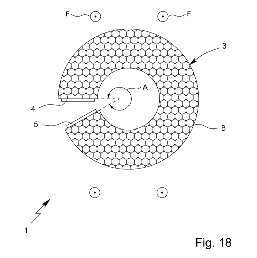
Fig. 18 schematically shows an eleventh embodiment in which the movement re-
gion B or guide device 3 is preferably formed by or comprises one or several,
in
particular at least essentially plane or flat, layers or strips of a van der
Waals heter-
ostructure or a layer thereof or a material based on a chemical element of the
ele-
ment of the fourth main group of the periodic table of elements, in particular
of gra-
phene. In the eleventh embodiment, the movement region B or guide device 3
preferably lies in a single plane. Preferably, the graphene strip or layer is
annular or
ring-like and/or forms a, preferably circular, section of a ring.
The field-generating means 10 (not shown in Fig. 18 to 22) is preferably
adapted to
create or apply the field F perpendicular to the plane of the movement region
B
and/or to the graphene strips/layer(s) or the plane defined by the latter, as
indicated
in Fig. 18.
Fig. 19 schematically shows a twelfth embodiment to which the above
explanations
concerning the eleventh embodiment preferably also apply.
In the twelfth embodiment, the movement region B or guide device 3 is
preferably
formed by at least one layer or strip of graphene which forms a helix, in
particular
CA 03087821 2020-07-07
WO 2019/141677 PCT/EP2019/050936
- 31 -
around a common or central axis C. In particular, the guide device 3 or
movement
region B is arranged screw-like or helix-like and/or forms a corkscrew way.
A "helix" preferably is a structure or object winding around a linear and/or
central
axis with a constant distance to that axis. A helix preferably winds around
the axis
with a constant slope.
As an alternative, which is not shown in Fig. 19, the movement region B or
guide
device 3 can preferably be formed by at least one layer or strip of graphene
which
forms a spiral, in particular around the axis C. In particular, the guide
device 3 or
movement region B is arranged spiral-like.
A "spiral" preferably is a structure or object winding around a point or
linear and/or
central axis with a decreasing or increasing distance to that point or axis.
Two-
dimensional spirals extend in a plane, whereas three-dimensional spirals
extend in
a direction parallel to the axis.
The graphene layer or strip shown in Fig. 18 to 20 preferably has a preferably
con-
stant width and a length, the length being larger or a multiple of the width.
Preferably, the graphene layer or strip is arranged such that the width
extends per-
pendicular to the axis C.
Preferably, different sections of the movement region B or guide device 3 are
ar-
ranged on top of another along the direction of the axis C in this case. A
surface or
flat side of the graphene layer/strip and/or a plane defined thereby is
preferably ar-
ranged at least essentially perpendicularly to the axis C.
Preferably, the slope of the helix-like or spiral-like movement region B or
guide de-
vice 3, in particular the graphene layer or strip, is less than 10 , more
preferably
less than 5 , particularly less than 2 , in particular less than 10
.
The field-generating means 10 is preferably adapted to create or apply the
field F
parallel to the axis C and/or at least essentially perpendicular to the plane
of the
movement region B and/or to the graphene layer(s) or the plane defined by the
lat-
ter, as indicated in Fig. 19. Preferably, the angle between the field F and
the plane
of the movement region and/or graphene layer or strip derives less than 10 ,
more
CA 03087821 2020-07-07
WO 2019/141677 PCT/EP2019/050936
- 32 -
preferably less than 5 , particularly less than 2 , in particular less than 1
from a
right angle.
Fig. 20 schematically shows a thirteenth embodiment. In this embodiment, the
movement region B or guide device 3 is preferably formed by spiral or a rolled-
up
layer or strip of graphene.
The guide device 3 or movement region B, in particular the graphene layer or
strip,
is preferably bent or arranged spiral-like around a central or common axis C.
Pref-
erably, a flat side, surface and/or the width of the graphene layer or strip
is ar-
ranged parallel to the axis C. In particular, the flat side or surface of the
graphene
layer or strip is bent such that the layer or strip does not define a plane.
The field-generating means 10 is preferably adapted to create or apply the
field F
parallel to the axis C and/or parallel to a flat side or surface of the
graphene layer or
strip. One of the connections 4, 5 is preferably arranged at an inner end and
the
other of the connections 4,5 is preferably arranged at an outer end of the
rolled-up
layer or strip.
Fig. 21 schematically shows a fourteenth embodiment. In the fourteenth embodi-
ment, the movement region B or guide device 3 comprises or is formed by a pref-
erably curved, angled or bent nanotube, in particular carbon nanotube, or
several
such nanotubes.
The (carbon) nanotube shown in Fig. 21, in particular its longitudinal axis,
is par-
ticularly bent or shaped as a ring or a section of a ring and/or not linearly
extending.
Preferably, the nanotube and/or its longitudinal axis is arranged at least
essentially
perpendicular to a central or common axis C and/or winds or bends around the
axis
C.
Preferably, the fourteenth embodiment only differs from the eleventh
embodiment
in that the movement region B or guide device 3 is formed by one or several
nano-
tubes instead of one or several at least essentially plane graphene layers or
strips.
Thus, the explanations made in connection with the eleventh embodiment prefera-
bly also apply to the fourteenth embodiment.
According to a fifteenth embodiment which is shown in particular in Fig. 22,
the
(carbon) nanotube forming the movement region B or guide device 3 or its
longitu-
CA 03087821 2020-07-07
WO 2019/141677 PCT/EP2019/050936
- 33 -
dinal axis can also form a spiral or helix around the axis C. In Fig. 22, the
nanotube
is helix-like or formed as a helix. However, it is also possible that the
nanotube is
spiral-like and/or formed as a spiral, as already explained with reference to
Fig. 19.
In the fourteenth and fifteenth embodiment, the field-generating means 10 is
pref-
erably adapted to create or apply the field F parallel to the axis C and/or at
least
essentially perpendicular to the nanotube and/or its longitudinal axis.
Preferably, the fifteenth embodiment is similar to the twelfth embodiment,
wherein a
(carbon) nanotube is used instead of a (graphene) layer or strip. All other
features
explained in connection with the twelfth embodiment preferably also apply to
the fif-
teenth embodiment.
The spirals and/or helices of the twelfth, thirteenth and/or fifteenth
embodiment can
also form several guide devices 3 and/or movement regions B, in particular
similar
or identical to the eighth and/or ninth embodiment and/or as explained with
refer-
ence to Fig. 13 and 14.
According to further embodiments which are not shown in the figures, it is in
princi-
pie also possible to use other materials which are similar to graphene, for
example
silicene, germanene or stanene, for forming the movement region B or guide
device
3. Likewise, as an alternative to carbon nanotubes, nanotubes formed of
silicon,
germanium or tin atoms can in principle be provided.
In general, it should be noted that, by means of the present invention, more
pre-
cisely the device 1 according to the invention and the method according to the
in-
vention, an asymmetrical or direction-dependent conductivity can be or is
generat-
ed (also called "nano-ratchet") and, accordingly, an electrical current, an
electrical
voltage, and/or an electrical power can be tapped or made available. In
particular, a
conversion of kinetic or thermal energy into electrical energy is made
possible in a
simple and efficient and/or direct manner.
In the following, the working principle of the device 1 is again explained
with refer-
ence in particular to Fig. 23 which very schematically shows the device 1. In
Fig.
23, a semi-circular movement region B with connections 4 and 5 is displayed.
In
addition, different paths P1, P2, P3 for the carriers 2 along the movement
region B
or main path H are indicated.
CA 03087821 2020-07-07
WO 2019/141677 PCT/EP2019/050936
- 34 -
In particular, movement of the carriers 2 in the device 1 or guide device 3 is
prefer-
ably determined by the initial direction of movement of the carriers 2, by the
exter-
nal field F acting on the carriers 2, by the number and type of reflections of
the car-
riers 2 at the flanks 9, and/or by the number and type of scattering events in
the
movement region B or along the main path H.
Without an external field F, the transmission probability for carriers 2
moving from
connection 4 to connection 5 is the same as for carriers moving in the
opposite di-
rection, i.e. from connection 5 to connection 4.
Assuming, for example, only "specular" reflection at the flanks 9 (i.e., angle
of inci-
dence equal to angle of reflection) and no scattering along the movement
region B
or main path H, the carriers 2 which are reflected at the flanks 9 follow the
path P1
which is schematically indicated in Fig. 23. In case of specular reflection at
the
flanks 9, the carriers 2 always move in the same direction along the movement
re-
gion B or main path H ("forward", from connection 4 to connection 5 in Fig.
23), be-
cause reversal of the movement direction does not take place during specular
re-
flections at the flanks 9, but the component of movement which is parallel to
the
flank 9 is conserved as the angle of incidence is equal to the angle of
reflection.
When an external static field F, for example a magnetic field, is applied, the
previ-
ous straight trajectories of the carriers 2 become curved trajectories
(indicated as
P2 and P3 in Fig. 23). A carrier 2 starting at connection 4 will move without
or at
least with very few reflections at the flanks 9 to the connection 5, provided
that the
external field is adjusted accordingly. This is shown by the path P2 in Fig.
23. Ac-
cordingly, the length of the path which the carrier 2 takes from connection 4
to con-
nection 5 is quite short. A carrier 2 starting at connection 5 under the same
condi-
tions will be able to move to connection 4 only with many reflections at the
flanks 9
so that the length of the path the carrier 2 takes from connection 5 to
connection 4
is quite long, accordingly.
Thus, the sum of the lengths of the paths P3 which a plurality of carriers 2
take
from connection 5 to connection 4 is preferably much longer than the sum of
the
lengths of the paths P2 of carriers 2 moving from connection 4 to connection
5.
Further, the flanks 9 can be at least partially diffusely scattering and/or
reflecting at
least partially non-specular manner and/or in a manner in which the
probability of
reflection to a certain angle does not follow a sine or cosine function, as
mentioned
CA 03087821 2020-07-07
WO 2019/141677 PCT/EP2019/050936
- 35 -
above. At such a non-specular reflection, the movement component of the
carrier 2
parallel to the flank 9 can be changed or reversed so that the carrier 2 can
even be
scattered "back", i.e. in a direction opposite the direction of movement of
the carrier
2 before the reflection or scattering. Further, the geometrical path which a
carrier 2
takes from connection 5 to connection 4 is longer than the geometrical path
from
connection 4 to connection 5. With a longer path of the carrier 2 within the
move-
ment region B, the probability for further scattering events within the
movement re-
gion B grows. In these further scattering events, the carrier 2 can also be
scattered
back.
By using a material with a sufficient mean-free path length for the carriers 2
in the
movement region B or main path H, the probability for scattering is extremely
low.
In conventional materials with a small mean free path length for the carriers
2, a
carrier 2 on the way from connection 4 to connection 5 would undergo a large
number of scattering events so that preferably no statistically relevant or
measura-
ble difference would be realized between the lengths of the path taken by
carriers 2
on the way from connection 4 to connection 5 and carriers 2 on the way from
con-
nection 5 to connection 4.
Thus, in conclusion, in the device 1 according to the proposal, a previously
ergodic
system (without external field F) is transformed to a non-ergodic system when
an
appropriate external field F is applied, the system having different
transmission
probabilities for carriers 2 moving from connection 4 to connection 5 then for
carri-
ers 2 moving from connection 5 to connection 4. Thus, the probability of
presence
for carriers 2 at the connection 5 is different, in the discussed example
according to
Fig. 23 higher, than the probability of presence for carriers 2 at the
connection 4.
This preferably leads to different, in particular electric, charges at the
connections
4, 5 and to voltages or electric powers which can be tapped via the
connections 4,
5.
As mentioned previously, individual aspects and features of the present
invention
and its various embodiments can be implemented individually and combined with
one another as desired.
CA 03087821 2020-07-07
WO 2019/141677
PCT/EP2019/050936
- 36 -
List of reference symbols:
1 device
2 carrier
3 guide device
4 connection
5 connection
6 layer/solid body
7 layer/solid body
8 boundary surface
9 flank
10 field-generating means
11 superconducting layer
12 leg
13 connection element
14 electrode/connecting device
15 intermediate region
16 intermediate layer
A central angle
B movement region
C common axis
D1 lateral extension/width (connecting device)
D2 lateral extension/width (guide device)
E plane
F field
H main path
P1 path
P2 path
P3 path
R radius of curvature
V1 vertical extension/height (guide device)
V2 vertical distance
W mean width
Z gyroradius of the carriers